EP1435640A2 - Electron beam writing equipment and method - Google Patents
Electron beam writing equipment and method Download PDFInfo
- Publication number
- EP1435640A2 EP1435640A2 EP03017075A EP03017075A EP1435640A2 EP 1435640 A2 EP1435640 A2 EP 1435640A2 EP 03017075 A EP03017075 A EP 03017075A EP 03017075 A EP03017075 A EP 03017075A EP 1435640 A2 EP1435640 A2 EP 1435640A2
- Authority
- EP
- European Patent Office
- Prior art keywords
- electron
- electron beam
- mark
- deflection
- beams
- Prior art date
- Legal status (The legal status is an assumption and is not a legal conclusion. Google has not performed a legal analysis and makes no representation as to the accuracy of the status listed.)
- Granted
Links
Images



Classifications
-
- H—ELECTRICITY
- H01—ELECTRIC ELEMENTS
- H01J—ELECTRIC DISCHARGE TUBES OR DISCHARGE LAMPS
- H01J37/00—Discharge tubes with provision for introducing objects or material to be exposed to the discharge, e.g. for the purpose of examination or processing thereof
- H01J37/30—Electron-beam or ion-beam tubes for localised treatment of objects
- H01J37/317—Electron-beam or ion-beam tubes for localised treatment of objects for changing properties of the objects or for applying thin layers thereon, e.g. for ion implantation
- H01J37/3174—Particle-beam lithography, e.g. electron beam lithography
-
- B—PERFORMING OPERATIONS; TRANSPORTING
- B82—NANOTECHNOLOGY
- B82Y—SPECIFIC USES OR APPLICATIONS OF NANOSTRUCTURES; MEASUREMENT OR ANALYSIS OF NANOSTRUCTURES; MANUFACTURE OR TREATMENT OF NANOSTRUCTURES
- B82Y10/00—Nanotechnology for information processing, storage or transmission, e.g. quantum computing or single electron logic
-
- B—PERFORMING OPERATIONS; TRANSPORTING
- B82—NANOTECHNOLOGY
- B82Y—SPECIFIC USES OR APPLICATIONS OF NANOSTRUCTURES; MEASUREMENT OR ANALYSIS OF NANOSTRUCTURES; MANUFACTURE OR TREATMENT OF NANOSTRUCTURES
- B82Y40/00—Manufacture or treatment of nanostructures
-
- H—ELECTRICITY
- H01—ELECTRIC ELEMENTS
- H01J—ELECTRIC DISCHARGE TUBES OR DISCHARGE LAMPS
- H01J37/00—Discharge tubes with provision for introducing objects or material to be exposed to the discharge, e.g. for the purpose of examination or processing thereof
- H01J37/30—Electron-beam or ion-beam tubes for localised treatment of objects
- H01J37/304—Controlling tubes by information coming from the objects or from the beam, e.g. correction signals
- H01J37/3045—Object or beam position registration
-
- H—ELECTRICITY
- H01—ELECTRIC ELEMENTS
- H01J—ELECTRIC DISCHARGE TUBES OR DISCHARGE LAMPS
- H01J37/00—Discharge tubes with provision for introducing objects or material to be exposed to the discharge, e.g. for the purpose of examination or processing thereof
- H01J37/30—Electron-beam or ion-beam tubes for localised treatment of objects
- H01J37/317—Electron-beam or ion-beam tubes for localised treatment of objects for changing properties of the objects or for applying thin layers thereon, e.g. for ion implantation
- H01J37/3174—Particle-beam lithography, e.g. electron beam lithography
- H01J37/3177—Multi-beam, e.g. fly's eye, comb probe
-
- H—ELECTRICITY
- H01—ELECTRIC ELEMENTS
- H01J—ELECTRIC DISCHARGE TUBES OR DISCHARGE LAMPS
- H01J2237/00—Discharge tubes exposing object to beam, e.g. for analysis treatment, etching, imaging
- H01J2237/30—Electron or ion beam tubes for processing objects
- H01J2237/304—Controlling tubes
- H01J2237/30433—System calibration
- H01J2237/3045—Deflection calibration
Definitions
- the present invention relates to an electron beam writing technique for use in a manufacturing process of a semiconductor integrated circuit. More specifically, the present invention relates to high-precision electron beam writing equipment and writing method.
- the size of the fastest deflection field on a sample is about 50 ⁇ m square (for example, Sakitani et al.: Journal of Vacuum and Technology, B12, 1992, pp. 2759-2763) .
- deflection is corrected. Specifically, an electron beam is deflected to near the corner of the deflection field to detect a mark for beam correction near it, thereby measuring and correcting a difference between a desired deflection distance and an actually measured deflection distance.
- Electron beam writing equipment having a micro deflection field of about 2 ⁇ m square is proposed (for example, see Iwadate et al.: Journal of Vacuum and Technology, B5, 1987, pp. 75-78).
- An object of the present invention is to provide an electron beam writing technique which can correct deflection for a micro field in electron beam writing equipment with high precision.
- the present invention has a function deflecting an electron beam at at least two different deflection speeds for scanning on a sample; a function repeating formation of a patterned beam in the electron beam by high speed scanning; a function moving the electron beam on a mark for beam correction by low speed scanning in synchronization with its one process; and a function detecting a backscattered electron or a secondary electron from the scanned mark for beam correction and near it or a transmission electron therethrough to correct the position or the deflection distance of the electron beam or blanking time from the detected result.
- the method according to the present invention is particularly suitable for multi-beam electron beam writing equipment. Correction using plural electron beams is effective.
- the electron beam writing equipment has a function moving adjacent electron beams in parallel to form a patterned beam; and a function comparing the detected results of the plural electron beams.
- the patterned beam is separately provided plural areas to perform higher-precision measurement. Further, as solving means, low speed scanning is performed in plural directions to change an on/off pattern of an electron beam at high speed scanning by the scanning direction.
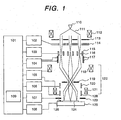
- FIG. 1 shows the configuration of electron beam writing equipment used in this embodiment.
- An electron beam 111 emitted from an electron gun (electron source) 110 is a parallel beam through a condenser lens 11.2, and is then divided into plural point beams by an aperture array 113 having plural apertures.
- a lens array 114 at the later stage forms intermediate images 116 of the point beams.
- a blanker array 115 and a blanking aperture 119 are provided so as to individually switch on/off the plural point beams.
- the multi point beams thus formed are condensed by a doublet lens 122 having a first projection lens 118 and a second projection lens 121 to be image formed onto a sample 124.
- the multi beams are distant from each other so as to provide large field projection in which the maximum distance of an electron beam on a pupil image is substantially longer than the maximum distance of the electron beam on an object plane.
- a deflector 120 for high speed and a deflector 128 for low speed to define the writing position on the sample 124.
- a mark 126 for detecting the position of an electron beam On a stage 125 is provided a mark 126 for detecting the position of an electron beam.
- the electron detector detecting a backscattered electron or a secondary electron from the mark 126 is used for measuring the position of an electron beam.
- An electron detector detecting an electron transmitted through an aperture mark may be also used.
- aligners 117 are provided above the first projection lens 118 as the first lens of the doublet lens 122. They are engaged with each other to adjust the incident angle and the incident position of an electron beam upon the lens.
- the aligners 117 are driven by an aligner control circuit 104.
- the doublet lens 122 is driven by a lens control circuit 105.
- electric currents are supplied.
- the set value of each of the electric currents is decided by information given by a data control circuit 101.
- a focus control circuit 102 and a pattern generating circuit 103 supply a voltage to operate the corresponding optical device. The set values of these are also decided by information given by the data control circuit 101.
- the data control circuit 101 uses information obtained from a signal handling circuit 107 and a stage control circuit 108 to perform calculation deciding the amounts of operation of the lenses and the aligners.
- This equipment has a display 109 having a screen making use of these functions to set the change of excitation, display the amount of change of the position of an electron beam, or reset the aligners and lens excitation currents.
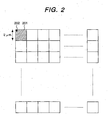
- the pitch of multi beams 202 of this embodiment on the sample is 2 ⁇ m.
- Each of the beams must write a micro field 201 of 2 ⁇ m square.
- on/off of an electron beam is controlled during 2 ⁇ m square writing to form a pattern.
- the micro field must be deflection scanned at high speed.
- a special deflector scans it.
- the following means is used.
- FIG. 3 shows its scanning method. High speed scanning 301 is performed on the entire surface of the micro field 201. The two-dimensional scanning process is repeated. Low speed scanning 303 is performed on a mark for beam correction 302 of 0.1 ⁇ m circle formed on a silicon substrate 304 provided on the stage 125 in engagement with (in synchronization with) one process (one cycle) of the scanning process. Summation of one cycle of high speed scanning is considered, which is equal to the electron beam of 2 ⁇ m square.
- the present invention is based on new findings in consideration of substantially converting a deflection field to a beam shape.
- two-dimensional scanning is performed on the mark for beam correction 302 by the low speed scanning 303.
- a rectangular beam image of 2 ⁇ m square can be obtained.
- the size of the image is measured to perform deflection correction of the micro field.
- the on/off control of an electron beam during scanning can form an electron beam image of a substantially arbitrary shape.
- Linearity of deflection can be also measured.
- FIG. 4 shows measured results of linearity.
- the horizontal axis indicates a desired design deflection distance ( ⁇ m) and the vertical axis indicates a difference between an actually measured deflection distance and the design deflection distance. Deflection in the X direction obtains a large gain, and deflection in the Y direction obtains a small gain. The result is fed back to finally reduce an error of the linearity below 5nm.
- Image shape measurement corresponds, not only to a rectangular pattern, but also to an arbitrary pattern.
- the means can inspect writing data and measure the limit of a blanking speed.
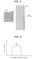
- a knife edge 502 as shown in FIG. 5 is used as a mark for detection.
- Gallium arsenide is used as the material of'the knife edge 502.
- a Faraday cup is used to detect and differentiate a detected signal of a transmission electron, thereby obtaining a beam profile.
- Low speed scanning in this case is substantially one-dimensional scanning.
- High speed scanning 501 is performed on the entire surface of the micro field 201.
- the two-dimensional scanning process is repeated.
- Low speed scanning 503 is performed on the knife edge 502 in engagement with (in synchronization with) one process (one cycle) of the scanning process.
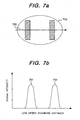
- FIG. 6 shows a beam profile obtained by the scanning method shown in FIG. 5.
- the horizontal axis indicates a low speed scanning distance and the vertical axis indicates the signal intensity of a detected transmission electron.
- the resolution of the knife edge 502 is sufficiently high.
- the tilt of the edge is caused mainly by unfocusing of the beam. This is used to adjust a stigma and a focal point.
- unfocusing of the beam can be measured in the state close to actual writing. This can obtain ⁇ 0.2 ⁇ m as reproducibility of focal point correction.
- FIG. 7a is an example in which the pattern of a micro field having a shape 702 so as to switch on/off a beam in separately provided two areas is used for measurement in a scanning direction 703 as shown in FIG. 7b.
- a beam profile 701 is divided into two crests. The distance of its peak is measured to correct high speed deflection. Measuring the center of the crest can increase the precision more easily than measuring the width of the crest. This is a correction method making use of the characteristic of this writing method.
- the on position in scanning in the 90° right angle direction, the on position may be changed during high speed operation.
- plural multi beams are used.
- high speed scanning 801 is performed on the entire surface of the micro field 201 by moving adjacent multi beams in parallel. As seen in the drawing, this can form a rectangular beam of about 2 ⁇ m ⁇ 4 ⁇ m by high speed scanning of one cycle.
- connection of the boundary parts is not complete.
- the distance between the two multi beams is short and the micro fields are overlapped at the boundary parts to make an overlap area 804. As a result, the intensity uniformity of the synthesized beam is deteriorated.
- This embodiment uses a backscattered electron signal produced by forming a tungsten dot 802 of 0.15 ⁇ m on the silicon thin film substrate 304 to be low speed scanned thereon. A signal intensity distribution thus obtained is resolved to write the boundary part of the micro field with high precision. The origin point position of each of the multi beams is corrected by adjusting lens excitation and the intensity of a rotating coil. An error of connection of the boundary areas can be below 5nm.
- Measurement using plural beams is important. The results of individually measured plural beams are compared to enable adjustment and monitoring of uniformity in multi beam writing.
- the present invention can correct a micro field of electron beam writing equipment with high precision.
- deflection scanning as the concept of the present invention is used for conversion to a beam shape.
- Various elements such as a focal point, a stigma and an origin point position can be adjusted.
- the present invention can realize electron beam wiring equipment and writing method which can correct deflection for a micro field of the electron beam writing equipment with high precision.
Landscapes
- Chemical & Material Sciences (AREA)
- Engineering & Computer Science (AREA)
- Nanotechnology (AREA)
- Analytical Chemistry (AREA)
- Physics & Mathematics (AREA)
- Crystallography & Structural Chemistry (AREA)
- Theoretical Computer Science (AREA)
- Mathematical Physics (AREA)
- Condensed Matter Physics & Semiconductors (AREA)
- General Physics & Mathematics (AREA)
- Manufacturing & Machinery (AREA)
- Electron Beam Exposure (AREA)
- Exposure And Positioning Against Photoresist Photosensitive Materials (AREA)
Abstract
Description
Claims (12)
- Electron beam writing equipment comprising:an electron source; an electron optics system irradiating for scanning an electron beam emitted from said electron source on a sample via deflection means having at least two different deflection speeds and an objective lens to form a desired pattern on said sample; a stage mounting said sample; a mark for beam correction provided on said stage; an electron detector detecting a backscattered electron, a secondary electron or a transmission electron obtained by irradiation of said electron beam; a function moving said electron beam by high speed scanning with said deflection means to repeat formation of a patterned beam; a function moving said electron beam on said mark for beam correction by low speed scanning with said deflection means in synchronization with one cycle of said repetition; and a function detecting a backscattered electron or a secondary electron emitted from said mark for beam correction and near it by said low speed scanning or a transmission electron transmitted through said mark for beam correction to correct the position or the deflection distance of said electron beam or blanking time from said detected result.
- The electron beam writing equipment according to claim 1, wherein said electron beams are multi beams having plural electron beams arrayed at a predetermined pitch, and said plural electron beams are used to perform correction.
- The electron beam writing equipment according to claim 2, wherein the adjacent electron beams of said multi beams are moved in parallel to form said patterned beam.
- The electron beam writing equipment according to claim 2, further comprising means comparing the detected results of said plural electron beams.
- The electron beam writing equipment according to claim 1, wherein said deflection means has a deflector for high speed scanning and a deflector for low speed scanning.
- The electron beam writing equipment according to claim 1, wherein said patterned beam has separately provided plural areas.
- The electron beam writing equipment according to claim 1, wherein said patterned beam is formed in a deflection area of substantially 2µm square.
- Electron beam writing equipment comprising:an electron optics system irradiating for scanning plural electron beams arrayed at a predetermined pitch on a sample via deflection means having plural deflectors having at least two different deflection speeds and an objective lens to form a desired pattern on said sample; a stage mounting said sample; a mark for beam correction provided on said stage; and an electron detector detecting a backscattered electron, a secondary electron or a transmission electron obtained by irradiation of said electron beam, wherein said deflection means has a first deflector for high speed scanning and a second deflector for low speed scanning, said plural electron beams are moved in parallel by high speed scanning with said first deflector to form a patterned beam, said plural electron beams are moved in parallel on said mark for beam correction by low speed scanning with said second deflector in synchronization with formation of said patterned beam, and a backscattered electron or a secondary electron emitted from said mark for beam correction and near it by said low speed scanning or a transmission electron transmitted through said mark for beam correction is detected to correct the position or the deflection distance of said electron beam or blanking time from said detected result.
- An electron beam writing method comprising the steps of: irradiating an electron beam emitted from an electron source on a sample via an electron optics system having deflection means having at least two different deflection speeds and an objective lens to form a desired pattern on said sample; high speed scanning said electron beam using said deflection means to repeat formation of a patterned beam; low speed scanning said electron beam on a mark for beam correction provided on a stage mounting said sample with said deflection means in synchronization with one cycle of said repetition; detecting a backscattered electron or a secondary electron emitted from said mark for beam correction and near it by said low speed scanning or a transmission electron transmitted through said mark for beam correction; and correcting the position or the deflection distance of said electron beam or blanking time from said detected result.
- The electron beam writing method according to claim 9, wherein said electron beams are multi beams having plural electron beams arrayed at a predetermined pitch, and said plural electron beams are used to perform correction.
- The electron beam writing method according to claim 10, wherein the adjacent electron beams of said multi beams are moved in parallel to form said patterned beam.
- The electron beam writing method according to claim 10, further comprising means comparing the detected results of said plural electron beams.
Applications Claiming Priority (2)
| Application Number | Priority Date | Filing Date | Title |
|---|---|---|---|
| JP2003000187 | 2003-01-06 | ||
| JP2003000187A JP4167904B2 (en) | 2003-01-06 | 2003-01-06 | Electron beam drawing apparatus and electron beam drawing method |
Publications (3)
| Publication Number | Publication Date |
|---|---|
| EP1435640A2 true EP1435640A2 (en) | 2004-07-07 |
| EP1435640A3 EP1435640A3 (en) | 2009-05-27 |
| EP1435640B1 EP1435640B1 (en) | 2013-02-27 |
Family
ID=32501166
Family Applications (1)
| Application Number | Title | Priority Date | Filing Date |
|---|---|---|---|
| EP03017075A Expired - Lifetime EP1435640B1 (en) | 2003-01-06 | 2003-07-28 | Electron beam writing equipment and method |
Country Status (3)
| Country | Link |
|---|---|
| US (2) | US6809319B2 (en) |
| EP (1) | EP1435640B1 (en) |
| JP (1) | JP4167904B2 (en) |
Cited By (6)
| Publication number | Priority date | Publication date | Assignee | Title |
|---|---|---|---|---|
| WO2016026664A1 (en) * | 2014-08-20 | 2016-02-25 | Arcam Ab | Energy beam size verification |
| WO2016026666A1 (en) * | 2014-08-20 | 2016-02-25 | Arcam Ab | Energy beam position verification |
| WO2016026663A1 (en) * | 2014-08-20 | 2016-02-25 | Arcam Ab | Energy beam deflection speed verification |
| CN109300759A (en) * | 2017-11-21 | 2019-02-01 | 聚束科技(北京)有限公司 | Low energy scanning electron microscope system, scanning electron microscope system and sample detection method |
| US12224153B2 (en) | 2020-12-02 | 2025-02-11 | Focus-Ebeam Technology (Beijing) Co., Ltd. | Electron microscope |
| US12315694B2 (en) | 2020-12-02 | 2025-05-27 | Focus-Ebeam Technology (Beijing) Co., Ltd. | Electron beam system |
Families Citing this family (12)
| Publication number | Priority date | Publication date | Assignee | Title |
|---|---|---|---|---|
| JP4477436B2 (en) * | 2004-06-30 | 2010-06-09 | キヤノン株式会社 | Charged particle beam exposure system |
| JP4583936B2 (en) * | 2005-01-06 | 2010-11-17 | 日本電子株式会社 | Charged particle beam device and control method of charged particle beam device |
| US7381970B2 (en) * | 2005-01-31 | 2008-06-03 | Summer Schneider | Specimen stage for charged-particle scanning microscopy |
| JP4907092B2 (en) | 2005-03-01 | 2012-03-28 | 株式会社日立ハイテクノロジーズ | Electron beam drawing apparatus and electron beam drawing method |
| JP4679978B2 (en) * | 2005-06-28 | 2011-05-11 | 株式会社日立ハイテクノロジーズ | Charged particle beam application equipment |
| JP5835892B2 (en) * | 2010-12-27 | 2015-12-24 | キヤノン株式会社 | Charged particle beam drawing apparatus and device manufacturing method |
| JP5843610B2 (en) * | 2011-12-28 | 2016-01-13 | キヤノン株式会社 | Drawing apparatus and article manufacturing method |
| EP3245666A4 (en) * | 2015-01-14 | 2018-08-22 | Intel Corporation | Underlying absorbing or conducting layer for ebeam direct write (ebdw) lithography |
| JP6863208B2 (en) * | 2017-09-29 | 2021-04-21 | 株式会社ニューフレアテクノロジー | Multi-charged particle beam drawing device and multi-charged particle beam drawing method |
| JP7160857B2 (en) * | 2020-05-20 | 2022-10-25 | 日本電子株式会社 | Beam adjustment method and three-dimensional additive manufacturing apparatus |
| US11183364B1 (en) * | 2020-06-12 | 2021-11-23 | Fei Company | Dual beam microscope system for imaging during sample processing |
| CN115188649A (en) * | 2022-06-22 | 2022-10-14 | 惠然科技有限公司 | Single electron beam time-sharing multiplexing device |
Citations (5)
| Publication number | Priority date | Publication date | Assignee | Title |
|---|---|---|---|---|
| US3900737A (en) | 1974-04-18 | 1975-08-19 | Bell Telephone Labor Inc | Electron beam exposure system |
| US4443703A (en) | 1981-02-23 | 1984-04-17 | Nippon Telegraph & Telephone Public Corporation | Method and apparatus of deflection calibration for a charged particle beam exposure apparatus |
| US5172331A (en) | 1989-12-18 | 1992-12-15 | Fujitsu Limited | Apparatus and method for effecting exposure of sample to charged particle beam |
| US5334846A (en) | 1991-07-02 | 1994-08-02 | Fujitsu Limited | Correction of charged particle beam exposure deflection by detecting stage position and a position detection mark |
| US6107636A (en) | 1997-02-07 | 2000-08-22 | Canon Kabushiki Kaisha | Electron beam exposure apparatus and its control method |
Family Cites Families (6)
| Publication number | Priority date | Publication date | Assignee | Title |
|---|---|---|---|---|
| JPH03270215A (en) * | 1990-03-20 | 1991-12-02 | Fujitsu Ltd | Charged particle beam exposure process and exposure device |
| JP3730263B2 (en) * | 1992-05-27 | 2005-12-21 | ケーエルエー・インストルメンツ・コーポレーション | Apparatus and method for automatic substrate inspection using charged particle beam |
| US5345085A (en) * | 1993-03-26 | 1994-09-06 | Etec Systems, Inc. | Method and structure for electronically measuring beam parameters |
| EP1369895B1 (en) * | 1996-03-04 | 2012-05-09 | Canon Kabushiki Kaisha | Electron beam exposure apparatus and method, and device manufacturing method |
| US6566885B1 (en) * | 1999-12-14 | 2003-05-20 | Kla-Tencor | Multiple directional scans of test structures on semiconductor integrated circuits |
| US7244932B2 (en) * | 2000-11-02 | 2007-07-17 | Ebara Corporation | Electron beam apparatus and device fabrication method using the electron beam apparatus |
-
2003
- 2003-01-06 JP JP2003000187A patent/JP4167904B2/en not_active Expired - Fee Related
- 2003-07-28 EP EP03017075A patent/EP1435640B1/en not_active Expired - Lifetime
- 2003-07-30 US US10/629,567 patent/US6809319B2/en not_active Expired - Fee Related
-
2004
- 2004-09-29 US US10/951,769 patent/US7049607B2/en not_active Expired - Fee Related
Patent Citations (5)
| Publication number | Priority date | Publication date | Assignee | Title |
|---|---|---|---|---|
| US3900737A (en) | 1974-04-18 | 1975-08-19 | Bell Telephone Labor Inc | Electron beam exposure system |
| US4443703A (en) | 1981-02-23 | 1984-04-17 | Nippon Telegraph & Telephone Public Corporation | Method and apparatus of deflection calibration for a charged particle beam exposure apparatus |
| US5172331A (en) | 1989-12-18 | 1992-12-15 | Fujitsu Limited | Apparatus and method for effecting exposure of sample to charged particle beam |
| US5334846A (en) | 1991-07-02 | 1994-08-02 | Fujitsu Limited | Correction of charged particle beam exposure deflection by detecting stage position and a position detection mark |
| US6107636A (en) | 1997-02-07 | 2000-08-22 | Canon Kabushiki Kaisha | Electron beam exposure apparatus and its control method |
Cited By (9)
| Publication number | Priority date | Publication date | Assignee | Title |
|---|---|---|---|---|
| WO2016026664A1 (en) * | 2014-08-20 | 2016-02-25 | Arcam Ab | Energy beam size verification |
| WO2016026666A1 (en) * | 2014-08-20 | 2016-02-25 | Arcam Ab | Energy beam position verification |
| WO2016026663A1 (en) * | 2014-08-20 | 2016-02-25 | Arcam Ab | Energy beam deflection speed verification |
| CN106573331A (en) * | 2014-08-20 | 2017-04-19 | 阿卡姆股份公司 | Energy beam size verification |
| CN109300759A (en) * | 2017-11-21 | 2019-02-01 | 聚束科技(北京)有限公司 | Low energy scanning electron microscope system, scanning electron microscope system and sample detection method |
| US10777382B2 (en) | 2017-11-21 | 2020-09-15 | Focus-Ebeam Technology (Beijing) Co., Ltd. | Low voltage scanning electron microscope and method for specimen observation |
| US11075056B2 (en) | 2017-11-21 | 2021-07-27 | Focus-Ebeam Technology (Beijing) Co., Ltd. | Scanning electron microscope objective lens system and method for specimen observation |
| US12224153B2 (en) | 2020-12-02 | 2025-02-11 | Focus-Ebeam Technology (Beijing) Co., Ltd. | Electron microscope |
| US12315694B2 (en) | 2020-12-02 | 2025-05-27 | Focus-Ebeam Technology (Beijing) Co., Ltd. | Electron beam system |
Also Published As
| Publication number | Publication date |
|---|---|
| US6809319B2 (en) | 2004-10-26 |
| JP2004214435A (en) | 2004-07-29 |
| US7049607B2 (en) | 2006-05-23 |
| US20040129898A1 (en) | 2004-07-08 |
| US20050040343A1 (en) | 2005-02-24 |
| EP1435640A3 (en) | 2009-05-27 |
| EP1435640B1 (en) | 2013-02-27 |
| JP4167904B2 (en) | 2008-10-22 |
Similar Documents
| Publication | Publication Date | Title |
|---|---|---|
| EP1435640B1 (en) | Electron beam writing equipment and method | |
| EP1302971B1 (en) | Method and device for the automatic generation of images adapted to align a charged particle beam column | |
| JP5497980B2 (en) | Charged particle beam application apparatus and sample inspection method | |
| JPH10214779A (en) | Electron beam exposure method and device manufacturing method using the method | |
| WO2003032351A2 (en) | Method and device for aligning a charged particle beam column | |
| US8785878B2 (en) | Charged particle beam apparatus | |
| JP4679978B2 (en) | Charged particle beam application equipment | |
| JPH09320931A (en) | Imaging characteristic measuring method and transfer apparatus using the method | |
| US7423274B2 (en) | Electron beam writing system and electron beam writing method | |
| JP4365579B2 (en) | Electron beam exposure apparatus and electron beam exposure method | |
| JP3983238B2 (en) | Electron beam drawing device | |
| US6606149B1 (en) | Optical system adjusting method for energy beam apparatus | |
| JP2021174615A (en) | Multi-beam image generation device and multi-beam image generation method | |
| US8847180B2 (en) | Charged particle beam apparatus, drawing apparatus, and method of manufacturing article | |
| JP2015095524A (en) | Drawing apparatus and article manufacturing method | |
| JP2002245960A (en) | Charged particle beam apparatus and device manufacturing method using such apparatus | |
| US20090206280A1 (en) | Charged-beam exposure apparatus having an improved alignment precision and exposure method | |
| JP2013183017A (en) | Drawing apparatus, reference element, and article manufacturing method | |
| JPWO2002075246A1 (en) | Pattern dimension measurement method | |
| JP2021182498A (en) | Multi-beam image generator and multi-beam image generation method | |
| JP3838771B2 (en) | Electron beam incident angle measuring method in electron beam exposure apparatus and exposure method using the same | |
| US6781680B1 (en) | Optical system adjusting method for energy beam apparatus | |
| JPH09330680A (en) | Electron beam exposure apparatus and electron beam exposure method | |
| JPH10199469A (en) | Electron beam illuminating device and electron beam exposure apparatus equipped with the device | |
| JP4026872B2 (en) | Position detection apparatus and electron beam exposure apparatus provided with the same |
Legal Events
| Date | Code | Title | Description |
|---|---|---|---|
| PUAI | Public reference made under article 153(3) epc to a published international application that has entered the european phase |
Free format text: ORIGINAL CODE: 0009012 |
|
| AK | Designated contracting states |
Kind code of ref document: A2 Designated state(s): AT BE BG CH CY CZ DE DK EE ES FI FR GB GR HU IE IT LI LU MC NL PT RO SE SI SK TR |
|
| AX | Request for extension of the european patent |
Extension state: AL LT LV MK |
|
| PUAL | Search report despatched |
Free format text: ORIGINAL CODE: 0009013 |
|
| AK | Designated contracting states |
Kind code of ref document: A3 Designated state(s): AT BE BG CH CY CZ DE DK EE ES FI FR GB GR HU IE IT LI LU MC NL PT RO SE SI SK TR |
|
| AX | Request for extension of the european patent |
Extension state: AL LT LV MK |
|
| 17P | Request for examination filed |
Effective date: 20091124 |
|
| 17Q | First examination report despatched |
Effective date: 20091214 |
|
| AKX | Designation fees paid |
Designated state(s): DE GB NL |
|
| GRAP | Despatch of communication of intention to grant a patent |
Free format text: ORIGINAL CODE: EPIDOSNIGR1 |
|
| RIN1 | Information on inventor provided before grant (corrected) |
Inventor name: OHTA, HIROYA, Inventor name: KAMIMURA, OSAMU, Inventor name: SOHDA, YASUNARI, Inventor name: GOTOH, SUSUMU, |
|
| GRAS | Grant fee paid |
Free format text: ORIGINAL CODE: EPIDOSNIGR3 |
|
| GRAA | (expected) grant |
Free format text: ORIGINAL CODE: 0009210 |
|
| AK | Designated contracting states |
Kind code of ref document: B1 Designated state(s): DE GB NL |
|
| REG | Reference to a national code |
Ref country code: GB Ref legal event code: FG4D |
|
| REG | Reference to a national code |
Ref country code: DE Ref legal event code: R096 Ref document number: 60343345 Country of ref document: DE Effective date: 20130425 |
|
| REG | Reference to a national code |
Ref country code: NL Ref legal event code: T3 |
|
| PLBE | No opposition filed within time limit |
Free format text: ORIGINAL CODE: 0009261 |
|
| STAA | Information on the status of an ep patent application or granted ep patent |
Free format text: STATUS: NO OPPOSITION FILED WITHIN TIME LIMIT |
|
| 26N | No opposition filed |
Effective date: 20131128 |
|
| REG | Reference to a national code |
Ref country code: DE Ref legal event code: R097 Ref document number: 60343345 Country of ref document: DE Effective date: 20131128 |
|
| PGFP | Annual fee paid to national office [announced via postgrant information from national office to epo] |
Ref country code: NL Payment date: 20150609 Year of fee payment: 13 |
|
| PGFP | Annual fee paid to national office [announced via postgrant information from national office to epo] |
Ref country code: DE Payment date: 20150722 Year of fee payment: 13 Ref country code: GB Payment date: 20150722 Year of fee payment: 13 |
|
| REG | Reference to a national code |
Ref country code: DE Ref legal event code: R119 Ref document number: 60343345 Country of ref document: DE |
|
| REG | Reference to a national code |
Ref country code: NL Ref legal event code: MM Effective date: 20160801 |
|
| GBPC | Gb: european patent ceased through non-payment of renewal fee |
Effective date: 20160728 |
|
| PG25 | Lapsed in a contracting state [announced via postgrant information from national office to epo] |
Ref country code: NL Free format text: LAPSE BECAUSE OF NON-PAYMENT OF DUE FEES Effective date: 20160801 Ref country code: DE Free format text: LAPSE BECAUSE OF NON-PAYMENT OF DUE FEES Effective date: 20170201 |
|
| PG25 | Lapsed in a contracting state [announced via postgrant information from national office to epo] |
Ref country code: GB Free format text: LAPSE BECAUSE OF NON-PAYMENT OF DUE FEES Effective date: 20160728 |