EP1435533A1 - Guide d'ondes et procédé de fabrication d'un guide d'ondes - Google Patents
Guide d'ondes et procédé de fabrication d'un guide d'ondes Download PDFInfo
- Publication number
- EP1435533A1 EP1435533A1 EP02425811A EP02425811A EP1435533A1 EP 1435533 A1 EP1435533 A1 EP 1435533A1 EP 02425811 A EP02425811 A EP 02425811A EP 02425811 A EP02425811 A EP 02425811A EP 1435533 A1 EP1435533 A1 EP 1435533A1
- Authority
- EP
- European Patent Office
- Prior art keywords
- core
- accordance
- wave guide
- melting point
- lower cladding
- Prior art date
- Legal status (The legal status is an assumption and is not a legal conclusion. Google has not performed a legal analysis and makes no representation as to the accuracy of the status listed.)
- Withdrawn
Links
Images


Classifications
-
- G—PHYSICS
- G02—OPTICS
- G02B—OPTICAL ELEMENTS, SYSTEMS OR APPARATUS
- G02B6/00—Light guides; Structural details of arrangements comprising light guides and other optical elements, e.g. couplings
- G02B6/10—Light guides; Structural details of arrangements comprising light guides and other optical elements, e.g. couplings of the optical waveguide type
- G02B6/12—Light guides; Structural details of arrangements comprising light guides and other optical elements, e.g. couplings of the optical waveguide type of the integrated circuit kind
- G02B6/13—Integrated optical circuits characterised by the manufacturing method
- G02B6/136—Integrated optical circuits characterised by the manufacturing method by etching
-
- G—PHYSICS
- G02—OPTICS
- G02B—OPTICAL ELEMENTS, SYSTEMS OR APPARATUS
- G02B6/00—Light guides; Structural details of arrangements comprising light guides and other optical elements, e.g. couplings
- G02B6/10—Light guides; Structural details of arrangements comprising light guides and other optical elements, e.g. couplings of the optical waveguide type
- G02B6/12—Light guides; Structural details of arrangements comprising light guides and other optical elements, e.g. couplings of the optical waveguide type of the integrated circuit kind
- G02B6/122—Basic optical elements, e.g. light-guiding paths
-
- G—PHYSICS
- G02—OPTICS
- G02B—OPTICAL ELEMENTS, SYSTEMS OR APPARATUS
- G02B6/00—Light guides; Structural details of arrangements comprising light guides and other optical elements, e.g. couplings
- G02B6/10—Light guides; Structural details of arrangements comprising light guides and other optical elements, e.g. couplings of the optical waveguide type
- G02B6/12—Light guides; Structural details of arrangements comprising light guides and other optical elements, e.g. couplings of the optical waveguide type of the integrated circuit kind
- G02B6/13—Integrated optical circuits characterised by the manufacturing method
- G02B6/132—Integrated optical circuits characterised by the manufacturing method by deposition of thin films
-
- G—PHYSICS
- G02—OPTICS
- G02B—OPTICAL ELEMENTS, SYSTEMS OR APPARATUS
- G02B6/00—Light guides; Structural details of arrangements comprising light guides and other optical elements, e.g. couplings
- G02B6/10—Light guides; Structural details of arrangements comprising light guides and other optical elements, e.g. couplings of the optical waveguide type
- G02B6/12—Light guides; Structural details of arrangements comprising light guides and other optical elements, e.g. couplings of the optical waveguide type of the integrated circuit kind
- G02B2006/12166—Manufacturing methods
- G02B2006/12173—Masking
Definitions
- the present invention concerns methods of manufacturing wave guides and the wave guides obtainable by means of that method.
- Known wave guides are integrated in a substrate, a silicon substrate for example, and comprise a buffer layer (also called, lower cladding), a core and an upper cladding.
- a buffer layer also called, lower cladding
- core the propagation of electromagnetic radiations within the core, typically at optical frequencies, is assured by doping the core in such a way as to make it assume a refractive index appropriately greater than the refractive index of the buffer and the upper cladding.
- the rectangular section does not assure an adequate independence of the losses in the wave guide from the polarization of the electromagnetic radiation that passes through it.
- radiation components of different polarization for example, in a simple case, TE and TM polarization
- PMD Polygonal Deformation
- international patent application WO 00/46618 describes a method of producing a wave guide comprising a core interposed between an upper and a lower cladding and integrated into a silica substrate.
- This international patent application affirms that a core of a circular section can be obtained by means of a heating phase that promotes the diffusion towards the interior of the claddings of any dopants present in the core.
- the core initially rectangular, comes to assume a circular section.
- the object of the present invention is to propose a method of manufacturing wave guides with a rounded section that will overcome the limits and disadvantages associated with the prior art techniques mentioned above.
- the object of the present invention is achieved by means of a method of manufacturing wave guides as defined in the annexed Claims 1 to 12.
- Another object of the present invention is to provided an integrated wave guide as defined by the annexed Claims 13 to 28.
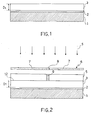
- a silicon oxide layer 2 is, preferably, grown on a substrate or wafer 1 (for example, made by silicon) a silicon oxide layer 2 is, preferably, grown.
- said oxide layer 2 can be obtained by means of a conventional oxidation technique such as, for example, wet thermal oxidation.
- This oxide layer 2 may have a thickness comprised, for example, between 0.2 and 1.0 ⁇ m. As will be evident to a person skilled in the art, the oxide layer 2 will be convenient as a layer intermediate between the silicon of substrate 1 and a layer of silicon dioxide to be subsequently deposited, because this will assure necessary continuity between the two employed materials.
- an intermediate or buffer layer 3 that performs the function of lower cladding of the wave guide to be realized.
- Said buffer 3 is preferably formed in substantially pure silica (silicon dioxide).
- the buffer 3 is made by silica containing impurities with a concentration of less than 1% by weight.
- the buffer 3 is realized with silica containing impurities with a concentration of less than 0.5% by weight.
- the buffer it is preferable for the buffer to have a high melting point and, for example, equal or close to the melting point of pure silica.
- the silica may be doped with ions - phosphorous and boron ions, for example - but this will cause a lowering of the melting point as compared with the melting point of pure silica.
- the buffer 3 has a melting point Tf 3 that is substantially comprised between 1300°C and 1350°C.
- the buffer 3 is such as to have a refractive index N 3 of an appropriate value that takes due account of the refractive index N 2 of the oxide layer 2.
- the refractive index N 3 is equal to 1.4575 ⁇ 0.001 measured at a wavelength amounting to 632 nm.
- the buffer 3 may be obtained by means of a deposition of silica on top of the oxide layer 2,
- the deposition technique will be the so-called PECVD (Plasma Enhanced Chemical Vapour Deposition) technique.
- the buffer 3 can be carried out a consolidation phase of the buffer 3, which can be realized by means of heating (annealing) in a furnace.
- the buffer 3 may be heated in an appropriate furnace to a temperature comprised between 1000 and 1300°C.
- the thickness D1 of the buffer 3 is, preferably, comprised between 8 and 30 ⁇ m.
- a mask 6 in glass, for example, appropriately treated in such a manner as to have opaque zones 7 and at least one transparent zone 8.
- the mask 6 is then placed in front of the photoresist layer 5 in such a way that the transparent zone 8 comes to be a zone of the buffer 3 intended to contain at least a part of the core of the wave guide.
- the mask 6 is exposed to an electromagnetic radiation S of an appropriate wavelength (ultraviolet radiation, for example) that, passing through the transparent zone, will strike and polymerize a portion 9 of the photoresist 5. This is followed by a conventional phase of developing the photoresist 5, during which the portion 9 is removed by means of a suitable chemical etching.
- an electromagnetic radiation S of an appropriate wavelength ultraviolet radiation, for example
- the opening 10 extends in a direction parallel to the axis of propagation of the wave guide that is to be obtained and may be, for example, rectangular in plan. Its cross section (with respect to the axis of propagation) has a shorter side d that is particularly small and may be equal to 1 ⁇ m, for example.
- the buffer 3 is etched through the opening 10. This etching is realized in order to remove portions of the buffer 3 in such a way as to define within the buffer a hollow or concave and preferably semi-cylindrical region 4 (delimited by a curved surface 11) that extends along the wave guide propagation axis.
- This curved surface 11 extends from the upper surface 12 of the buffer 3, i.e. the surface opposite the oxide layer 2, towards the interior of the buffer and is joined to this upper surface 12.
- the surface 11 has a section that is substantially circular, the radius R of that section being smaller than the thickness D1 of the buffer 3.
- the radius R may be comprised in the range between 1 and 4 ⁇ m to obtain a wave guide core having a diameter of 2-8 ⁇ m.
- an isotropic etching is performed, i.e. a chemical agent capable of etching the buffer 3 at comparable or substantially identical speeds in a vertical direction V and a lateral direction (perpendicular to the previous one) is used.
- a chemical agent capable of etching the buffer 3 at comparable or substantially identical speeds in a vertical direction V and a lateral direction (perpendicular to the previous one) is used.
- the etching will proceed in the vertical direction V in a manner altogether similar to what is being done in the lateral direction.
- this isotropic etching can be a wet etching employing a solution capable of etching silicon dioxide such as - for example - an ammonium fluoride and hydrofluoric acid (HF) based solution.
- a solution capable of etching silicon dioxide such as - for example - an ammonium fluoride and hydrofluoric acid (HF) based solution.
- solutions other than those just mentioned may also be employed for the isotropic etching step, including - for example - a water and hydrofluoric acid based solution or other solutions that persons skilled in the art generically refer to as "buffered solutions”.
- the substrate 1 is placed in the aforementioned solution for such time as may be needed for the solution to attack the surface of the buffer 3 exposed by the opening 10 and incise the buffer in the desired manner.
- the curved surface 11 may be obtained by means of a dry isotropic etching, i.e. employing plasma.
- the substrate 1 is inserted in an appropriate reactor and a plasma in the gaseous phase is etches the surface of the buffer 3 exposed by the opening 10 to define the surface 11.
- the plasma employed may be constituted by nitrogen trifluoride (NF3) or by freon 114 (CF4).
- the core layer 13 fills the concave region 4 (of radius R) defined by the curved surface 11 within the buffer 3 and extends above the surface 12 of the buffer with a thickness D 2 (preferably different from zero) and, advantageously, correlated with the radius R of the semi-cylindrical concave region 4.
- the core layer 13 is obtained, for example, by depositing a material, preferably silica, that has been suitably doped (for example, with phosphorus ions, or phosphorus and boron ions, or germanium ions) in such a way that the core layer will have a refractive index N 13 greater than the refractive index N 3 of the buffer 3 and thus permit appropriate confinement of the electromagnetic radiation to be propagated in the wave guide.
- a material preferably silica, that has been suitably doped (for example, with phosphorus ions, or phosphorus and boron ions, or germanium ions) in such a way that the core layer will have a refractive index N 13 greater than the refractive index N 3 of the buffer 3 and thus permit appropriate confinement of the electromagnetic radiation to be propagated in the wave guide.
- the refractive index N 13 of the core layer 13 may be equal to the refractive index N 3 of the buffer 3 increased by an amount comprised between 0.15% and 1.5% of N 3 .
- the core layer 13 may be realized in silica doped with substances such as to lower its melting temperature Tf 13 .
- the core layer 13 is made by with a material such that its melting point Tf 13 will be lower than the melting point Tf 3 of the buffer 3 by an amount such as to substantially avoid the dopants included in this material diffusing into the interior of the buffer 3 when the temperature of this material is raised to its melting point Tf 13 .
- the difference between the melting point Tf 3 of the buffer 3 and the melting point Tf 13 of the core layer 13 is such that when the temperature of the structure of Figures 4-9 is brought up to the melting point Tf 13 , the buffer 3 (and, more particularly, the curved surface 11) will maintain the rounded shape (which may be semi-cylindrical, for example) of the concave region 4 obtained by means of the isotropic attack and, consequently, will not become appreciably deformed.
- the melting point Tf 3 of the buffer 3 and the melting point Tf 13 of the core layer 13 will differ by at least 150°C (for example, the temperature difference may be comprised between 150°C and 350°C). Even more preferably, the melting point Tf 3 of the buffer 3 and that of the core layer 13 will differ by at least 250°C (for example, the temperature difference may be comprised between 250°C and 350°C).
- the core layer 13 may include phosphorus as a dopant at a concentration comprised between 2% and 8% by weight, and preferably comprised between 2% and 4.7%. Suitable values for the melting point of the core layer 13 will be substantially comprised between 1110°C and 1200°C.
- the formation of the core layer 13 of Figure 4 includes the deposition of the core material on the upper surface 12 of the buffer 3 and subsequent steps of reheating (annealing) and cooling of the deposited layer and the entire structure in order to consolidate the core layer 13.
- the heating phase makes it possible to fill the cavity 4 formed in the buffer layer 3 and, at the same time, to level an upper surface 21 of the core layer 13. This levelling occurs because the material forming the core layer 13 is heated to a temperature close to its melting point Tf 13 , thereby permitting a part of the material to slide into the cavity 4, while yet maintaining the thickness of the core layer 13 at the desired value D 2 in the region around the cavity.
- the method in accordance with the invention continues with the deposition of a further layer of photoresist (not shown in the figure) on a free surface 14 of the core layer 13. This is followed by a step in which this photoresist layer is irradiated (using an appropriately treated mask) and a part of the photoresist layer is removed (developed) in such a way as to define the photoresist portion 15 shown in Figure 5.
- the method in accordance with the invention continues with a phase of anisotropic etching of the core layer 13, which can be carried out by means of conventional dry etching techniques.
- This etching is carried out in such a way as to remove portions of the core layer 13, thereby defining an upper core portion 16 (having, for example, a rectangular section) that extends above the upper surface 12 of the buffer 3 and a lower core portion 17 having a section of the semi-circular type and situated inside the concave region 4 defined by the curved surface 11.
- the upper core portion 16 will have a vertical axis of symmetry A-A passing through the centre C of the semi-circular section corresponding to the curved surface 11.
- a step of melting the upper and lower core portions 16 and 17 is carried out.
- the buffer 3 remains in the solid state and the concave region 4 and, more particularly, the rounded surface 11 maintains the shape obtained by means of the isotropic attack. Furthermore, the face of the buffer 3 corresponding to the rounded surface 11 of the concave region 4 performs a function of containing the molten material that constitutes the lower portion 17 of the core and assures that the material of the core will remain separate from that of the buffer 3.
- the material constituting the upper core portion 16 is free (i.e. is not enclosed between adjacent faces), it will tend to assume a configuration during the melting phase such as to reduce the surface energy to a minimum and will therefore assume a shape having a circular arc, preferably a semicircle, as its section.
- the diffusion of dopant from the upper and lower core portions 16 and 17 towards the buffer can be particularly minimized by carrying out the aforesaid heat treatment (i.e. heating to the temperature Tf 13 and the subsequent cooling) with an adequate rate of change of temperature in the course of time.
- the aforesaid heat treatment should be carried out rapidly.
- the heating up to the melting point Tf 13 is carried out in about 60 seconds, after which the structure is first left at the temperature Tf 13 for about another 60 seconds (in such a way as to render possible the desired collapse of the material) and then cooled down to room temperature in about another 60 seconds.
- This temperature change pattern can be obtained by carrying out the heat treatment with the help of conventional RTPM (Rapid Thermal Processor Machine) equipment.
- RTPM Rapid Thermal Processor Machine
- Equipment of this type is marketed, among others by Messrs. Applied Materials, USA.
- an upper cladding layer 19 is deposited on the free surface 4 of the buffer 3 and on the core 18.
- This upper cladding 19 is realized in silica appropriately doped so as to obtain a refractive index N 19 substantially equal to the refractive index N 2 of the buffer 3 and a melting point Tf 19 appropriately lower than the melting point of the buffer 3 and the core 18.
- an adequate refractive index N 19 can be obtained by appropriately dosing such dopants as phosphorus, which will cause the refractive index to go up as its concentration increases, and boron, which will cause the refractive index to diminish as its concentration becomes greater.
- both the phosphorus and the boron will cause the melting point of the upper buffer 19 to diminish as their concentration in the silica increases.
- the melting point Tf 19 of the upper cladding 19 will differ from the melting point Tf 13 of the core 13 by at least 100°C (for example, the temperature difference Tf 13 - Tf 19 will be comprised between 100°C and 450°C). More preferably, the melting point Tf 19 will differ from the temperature Tf 13 by at least 250°C (for example, the temperature difference Tf 13 - Tf 19 will be comprised between 250°C and 450°C).
- the melting point Tf 19 of the upper cladding 19 will be comprised between 800 and 1000°C and, preferably, between 880 and 930°C, for example 900°C.
- the structure of Figure 9 is subjected to a thermic treatment to consolidate the upper cladding 19 in such a way as to confer the desired thermomechanical properties upon the cladding and the entire structure and to assure their stability during the life of the device.
- the structure of Figure 9 will be subjected to an annealing treatment that includes heating to a temperature close to or greater than the melting point of the upper cladding 19, followed by appropriate cooling.
- this heating step will neither cause the core 18 to melt nor lead to any substantial deformation of the buffer 3, nor will there be any substantial diffusion of material from the core 18 to the buffer 3.
- the core 18 of this guide has a section that defines a rounded profile both within the upper cladding 19 and within the buffer 3.
- the described method makes it possible to obtain wave guides having cores with an ovoidal, substantially ellipsoidal and, as already said, substantially circular section.
- the method of the invention is particularly advantageous, because it does not comprise phases of excessive complexity. Furthermore, this method is compatible with the previously developed integration techniques on silicon and makes it possible to obtain accuracies greater than those obtainable with the known methodologies.
- the teachings of the present invention can be applied also to materials other than silicon and silica that are suitable for the propagation of electromagnetic waves and can be employed for the production of integrated wave guides.
Landscapes
- Physics & Mathematics (AREA)
- Engineering & Computer Science (AREA)
- Microelectronics & Electronic Packaging (AREA)
- General Physics & Mathematics (AREA)
- Optics & Photonics (AREA)
- Optical Integrated Circuits (AREA)
Priority Applications (2)
| Application Number | Priority Date | Filing Date | Title |
|---|---|---|---|
| EP02425811A EP1435533A1 (fr) | 2002-12-30 | 2002-12-30 | Guide d'ondes et procédé de fabrication d'un guide d'ondes |
| US10/744,062 US20040152020A1 (en) | 2002-12-30 | 2003-12-22 | Wave guide manufactoring method and wave guide |
Applications Claiming Priority (1)
| Application Number | Priority Date | Filing Date | Title |
|---|---|---|---|
| EP02425811A EP1435533A1 (fr) | 2002-12-30 | 2002-12-30 | Guide d'ondes et procédé de fabrication d'un guide d'ondes |
Publications (1)
| Publication Number | Publication Date |
|---|---|
| EP1435533A1 true EP1435533A1 (fr) | 2004-07-07 |
Family
ID=32479864
Family Applications (1)
| Application Number | Title | Priority Date | Filing Date |
|---|---|---|---|
| EP02425811A Withdrawn EP1435533A1 (fr) | 2002-12-30 | 2002-12-30 | Guide d'ondes et procédé de fabrication d'un guide d'ondes |
Country Status (2)
| Country | Link |
|---|---|
| US (1) | US20040152020A1 (fr) |
| EP (1) | EP1435533A1 (fr) |
Cited By (1)
| Publication number | Priority date | Publication date | Assignee | Title |
|---|---|---|---|---|
| US20160197067A1 (en) * | 2012-11-07 | 2016-07-07 | Taiwan Semiconductor Manufacturing Company, Ltd. | Contoured Package-on-Package Joint |
Citations (6)
| Publication number | Priority date | Publication date | Assignee | Title |
|---|---|---|---|---|
| US4384038A (en) * | 1980-11-25 | 1983-05-17 | U.S. Philips Corporation | Method of producing integrated optical waveguide circuits and circuits obtained by this method |
| JPS59101605A (ja) * | 1982-12-01 | 1984-06-12 | Hitachi Ltd | 光導波路 |
| JPS60129711A (ja) * | 1983-12-16 | 1985-07-11 | Oki Electric Ind Co Ltd | 光導波路形成方法 |
| JPS61210304A (ja) * | 1985-03-15 | 1986-09-18 | Nippon Sheet Glass Co Ltd | 光平面導波路の製造方法 |
| JPH01191804A (ja) * | 1988-01-28 | 1989-08-01 | Teijin Seiki Co Ltd | 光導波路及びその製造方法 |
| JPH0442216A (ja) * | 1990-06-08 | 1992-02-12 | Fuji Photo Film Co Ltd | 有機単結晶光導波路の製造方法 |
Family Cites Families (7)
| Publication number | Priority date | Publication date | Assignee | Title |
|---|---|---|---|---|
| US4339173A (en) * | 1975-09-08 | 1982-07-13 | Corning Glass Works | Optical waveguide containing P2 O5 and GeO2 |
| US5033815A (en) * | 1979-10-25 | 1991-07-23 | Nippon Telephone & Telegraph | Optical transmission fiber and process for producing the same |
| US4425146A (en) * | 1979-12-17 | 1984-01-10 | Nippon Telegraph & Telephone Public Corporation | Method of making glass waveguide for optical circuit |
| US5064266A (en) * | 1990-07-05 | 1991-11-12 | Photonic Integration Research, Inc. | Circular channel waveguides and lenses formed from rectangular channel waveguides |
| US5546480A (en) * | 1995-04-28 | 1996-08-13 | Texas Instruments Incorporated | Hybrid all optical silica waveguide modulator using non-linear electro-optic components |
| GB2346452A (en) * | 1999-02-05 | 2000-08-09 | Univ Glasgow | Waveguides |
| US6624077B2 (en) * | 2001-12-17 | 2003-09-23 | Applied Materials, Inc. | Integrated circuit waveguide |
-
2002
- 2002-12-30 EP EP02425811A patent/EP1435533A1/fr not_active Withdrawn
-
2003
- 2003-12-22 US US10/744,062 patent/US20040152020A1/en not_active Abandoned
Patent Citations (6)
| Publication number | Priority date | Publication date | Assignee | Title |
|---|---|---|---|---|
| US4384038A (en) * | 1980-11-25 | 1983-05-17 | U.S. Philips Corporation | Method of producing integrated optical waveguide circuits and circuits obtained by this method |
| JPS59101605A (ja) * | 1982-12-01 | 1984-06-12 | Hitachi Ltd | 光導波路 |
| JPS60129711A (ja) * | 1983-12-16 | 1985-07-11 | Oki Electric Ind Co Ltd | 光導波路形成方法 |
| JPS61210304A (ja) * | 1985-03-15 | 1986-09-18 | Nippon Sheet Glass Co Ltd | 光平面導波路の製造方法 |
| JPH01191804A (ja) * | 1988-01-28 | 1989-08-01 | Teijin Seiki Co Ltd | 光導波路及びその製造方法 |
| JPH0442216A (ja) * | 1990-06-08 | 1992-02-12 | Fuji Photo Film Co Ltd | 有機単結晶光導波路の製造方法 |
Non-Patent Citations (8)
| Title |
|---|
| BOULAS C ET AL: "LOW LOSS MULTIMODE WAVEGUIDES ON SILICON SUBSTRATE", ELECTRONICS LETTERS, IEE STEVENAGE, GB, vol. 28, no. 17, 13 August 1992 (1992-08-13), pages 1648 - 1649, XP000315891, ISSN: 0013-5194 * |
| GROSSE ET AL: "deep wet eching of fused silica glass for hollow capillary optical leaky waveguides in microfluidic devices", JOURNAL OF MICROMECHANICS AND MICROENGINEERING, vol. 11, 2001, pages 257 - 262, XP020068644 * |
| PATENT ABSTRACTS OF JAPAN vol. 008, no. 219 (P - 306) 5 October 1984 (1984-10-05) * |
| PATENT ABSTRACTS OF JAPAN vol. 009, no. 292 (P - 406) 19 November 1985 (1985-11-19) * |
| PATENT ABSTRACTS OF JAPAN vol. 011, no. 040 (P - 544) 5 February 1987 (1987-02-05) * |
| PATENT ABSTRACTS OF JAPAN vol. 013, no. 482 (P - 953) 2 November 1989 (1989-11-02) * |
| PATENT ABSTRACTS OF JAPAN vol. 016, no. 218 (P - 1357) 21 May 1992 (1992-05-21) * |
| SUN C J ET AL: "SILICA-BASED CIRCULAR CROSS-SECTIONED CHANNEL WAVEGUIDES", IEEE PHOTONICS TECHNOLOGY LETTERS, IEEE INC. NEW YORK, US, vol. 3, no. 3, 1 March 1991 (1991-03-01), pages 238 - 240, XP000202940, ISSN: 1041-1135 * |
Cited By (4)
| Publication number | Priority date | Publication date | Assignee | Title |
|---|---|---|---|---|
| US20160197067A1 (en) * | 2012-11-07 | 2016-07-07 | Taiwan Semiconductor Manufacturing Company, Ltd. | Contoured Package-on-Package Joint |
| US9991246B2 (en) * | 2012-11-07 | 2018-06-05 | Taiwan Semiconductor Manufacturing Company, Ltd. | Contoured package-on-package joint |
| US10672751B2 (en) | 2012-11-07 | 2020-06-02 | Taiwan Semiconductor Manufacturing Company, Ltd. | Contoured package-on-package joint |
| US11270990B2 (en) * | 2012-11-07 | 2022-03-08 | Taiwan Semiconductor Manufacturing Company, Ltd. | Contoured package-on-package joint |
Also Published As
| Publication number | Publication date |
|---|---|
| US20040152020A1 (en) | 2004-08-05 |
Similar Documents
| Publication | Publication Date | Title |
|---|---|---|
| EP0490095B1 (fr) | Méthode de fabrication d'un dispositif longiligne en optique intégrée comportant dans sa surface au moins un guide d'onde confiné latéralement | |
| JP2501395B2 (ja) | 光学装置とその形成方法 | |
| US6356694B1 (en) | Process for producing planar waveguide structures as well as waveguide structure | |
| US5563979A (en) | Erbium-doped planar optical device | |
| US5200029A (en) | Method of making a planar optical amplifier | |
| JP2002540451A (ja) | 導波路構造および導波路構造の形成方法 | |
| JPH0531124B2 (fr) | ||
| EP1435533A1 (fr) | Guide d'ondes et procédé de fabrication d'un guide d'ondes | |
| CN110095840A (zh) | 一种硅基浅刻蚀波导起偏器及其制备方法 | |
| JP2530823B2 (ja) | フアイバ型単一モ−ド光波回路素子及びその製造方法 | |
| JP3090293B2 (ja) | 光回路及びその製造方法 | |
| EP0622343A2 (fr) | Méthode pour augmenter d'indice de réfraction de matériau vitreux | |
| EP1151332A1 (fr) | Guide d'ondes pour un circuit optique et son procede de fabrication | |
| CN108646345A (zh) | 一种深紫外平面光波导制作方法 | |
| JP3245367B2 (ja) | 光導波路の形成方法 | |
| EP0762162A1 (fr) | Dispositif comprenant couplage fibre-guide d'onde planaire et son procédé de fabrication | |
| JP3836730B2 (ja) | 偏波保存フォトニッククリスタルファイバ及びその製造方法 | |
| US20050213916A1 (en) | Method of manufacturing optical waveguide device | |
| WO2020129664A1 (fr) | Guide d'ondes optique et son procédé de fabrication | |
| JPH0720336A (ja) | 光導波路の構造とその製造方法 | |
| Naik | Planar And Channel Waveguides Fabricated By Nitrogen Ion Implantation In Fused Silica | |
| JP2004301981A (ja) | シリコン基板とその形成方法 | |
| US20170329083A1 (en) | Method for manufacturing a photonic waveguide and photonic waveguide manufactured by said method | |
| Tréanton et al. | Engineering of waveguides and other micro-structures in dielectrics | |
| JP4372039B2 (ja) | 低伝播損失光導波路及びその作製方法 |
Legal Events
| Date | Code | Title | Description |
|---|---|---|---|
| PUAI | Public reference made under article 153(3) epc to a published international application that has entered the european phase |
Free format text: ORIGINAL CODE: 0009012 |
|
| AK | Designated contracting states |
Kind code of ref document: A1 Designated state(s): AT BE BG CH CY CZ DE DK EE ES FI FR GB GR IE IT LI LU MC NL PT SE SI SK TR |
|
| AX | Request for extension of the european patent |
Extension state: AL LT LV MK RO |
|
| 17P | Request for examination filed |
Effective date: 20041216 |
|
| 17Q | First examination report despatched |
Effective date: 20050110 |
|
| AKX | Designation fees paid |
Designated state(s): DE FR GB IT |
|
| 17Q | First examination report despatched |
Effective date: 20050110 |
|
| STAA | Information on the status of an ep patent application or granted ep patent |
Free format text: STATUS: THE APPLICATION IS DEEMED TO BE WITHDRAWN |
|
| 18D | Application deemed to be withdrawn |
Effective date: 20071123 |