EP1434426A2 - Camera module and manufacturing method thereof - Google Patents
Camera module and manufacturing method thereof Download PDFInfo
- Publication number
- EP1434426A2 EP1434426A2 EP03029192A EP03029192A EP1434426A2 EP 1434426 A2 EP1434426 A2 EP 1434426A2 EP 03029192 A EP03029192 A EP 03029192A EP 03029192 A EP03029192 A EP 03029192A EP 1434426 A2 EP1434426 A2 EP 1434426A2
- Authority
- EP
- European Patent Office
- Prior art keywords
- image sensor
- lens
- camera module
- bonded
- lenses
- Prior art date
- Legal status (The legal status is an assumption and is not a legal conclusion. Google has not performed a legal analysis and makes no representation as to the accuracy of the status listed.)
- Withdrawn
Links
Images




Classifications
-
- H—ELECTRICITY
- H04—ELECTRIC COMMUNICATION TECHNIQUE
- H04N—PICTORIAL COMMUNICATION, e.g. TELEVISION
- H04N23/00—Cameras or camera modules comprising electronic image sensors; Control thereof
- H04N23/50—Constructional details
- H04N23/54—Mounting of pick-up tubes, electronic image sensors, deviation or focusing coils
-
- H—ELECTRICITY
- H04—ELECTRIC COMMUNICATION TECHNIQUE
- H04N—PICTORIAL COMMUNICATION, e.g. TELEVISION
- H04N23/00—Cameras or camera modules comprising electronic image sensors; Control thereof
- H04N23/50—Constructional details
- H04N23/55—Optical parts specially adapted for electronic image sensors; Mounting thereof
-
- H—ELECTRICITY
- H10—SEMICONDUCTOR DEVICES; ELECTRIC SOLID-STATE DEVICES NOT OTHERWISE PROVIDED FOR
- H10F—INORGANIC SEMICONDUCTOR DEVICES SENSITIVE TO INFRARED RADIATION, LIGHT, ELECTROMAGNETIC RADIATION OF SHORTER WAVELENGTH OR CORPUSCULAR RADIATION
- H10F39/00—Integrated devices, or assemblies of multiple devices, comprising at least one element covered by group H10F30/00, e.g. radiation detectors comprising photodiode arrays
- H10F39/80—Constructional details of image sensors
- H10F39/804—Containers or encapsulations
-
- H—ELECTRICITY
- H10—SEMICONDUCTOR DEVICES; ELECTRIC SOLID-STATE DEVICES NOT OTHERWISE PROVIDED FOR
- H10F—INORGANIC SEMICONDUCTOR DEVICES SENSITIVE TO INFRARED RADIATION, LIGHT, ELECTROMAGNETIC RADIATION OF SHORTER WAVELENGTH OR CORPUSCULAR RADIATION
- H10F39/00—Integrated devices, or assemblies of multiple devices, comprising at least one element covered by group H10F30/00, e.g. radiation detectors comprising photodiode arrays
- H10F39/80—Constructional details of image sensors
- H10F39/806—Optical elements or arrangements associated with the image sensors
-
- H—ELECTRICITY
- H10—SEMICONDUCTOR DEVICES; ELECTRIC SOLID-STATE DEVICES NOT OTHERWISE PROVIDED FOR
- H10F—INORGANIC SEMICONDUCTOR DEVICES SENSITIVE TO INFRARED RADIATION, LIGHT, ELECTROMAGNETIC RADIATION OF SHORTER WAVELENGTH OR CORPUSCULAR RADIATION
- H10F77/00—Constructional details of devices covered by this subclass
- H10F77/40—Optical elements or arrangements
- H10F77/407—Optical elements or arrangements indirectly associated with the devices
-
- H—ELECTRICITY
- H10—SEMICONDUCTOR DEVICES; ELECTRIC SOLID-STATE DEVICES NOT OTHERWISE PROVIDED FOR
- H10F—INORGANIC SEMICONDUCTOR DEVICES SENSITIVE TO INFRARED RADIATION, LIGHT, ELECTROMAGNETIC RADIATION OF SHORTER WAVELENGTH OR CORPUSCULAR RADIATION
- H10F77/00—Constructional details of devices covered by this subclass
- H10F77/40—Optical elements or arrangements
- H10F77/413—Optical elements or arrangements directly associated or integrated with the devices, e.g. back reflectors
-
- H—ELECTRICITY
- H10—SEMICONDUCTOR DEVICES; ELECTRIC SOLID-STATE DEVICES NOT OTHERWISE PROVIDED FOR
- H10F—INORGANIC SEMICONDUCTOR DEVICES SENSITIVE TO INFRARED RADIATION, LIGHT, ELECTROMAGNETIC RADIATION OF SHORTER WAVELENGTH OR CORPUSCULAR RADIATION
- H10F77/00—Constructional details of devices covered by this subclass
- H10F77/50—Encapsulations or containers
Definitions
- This invention relates to a camera module and its manufacturing method, specifically to a small size camera module suitable to be incorporated into a portable device such as a mobile phone and a manufacturing method of such a device.
- FIG. 11 is a cross-sectional view showing a structure of such a camera module.
- Fig. 11 shows a lens-barrel 50, a lens 51 mounted inside the lens-barrel 50 and an IR filter 52 to block infrared radiation attached to a mouth of the lens-barrel 50. It also shows an image sensor chip 60 housed in a space within the lens-barrel 50 and electrically connected to a printed circuit board 70.
- the image sensor chip 60 converts light incident from a photogenic subject through the IR filter 52 and the lens 51 into electric signals.
- CCDs Charge Coupled Devices
- a supporting glass substrate 62 is bonded to the silicon chip 61 to bolster it in the image sensor chip 60.
- Each of redistribution wirings 64A and 64B is formed extending from each of electrode pads 63A and 63B, which are formed on a peripheral surface of the image sensor chip 60, over a side surface and to a back surface of the silicon chip 61.
- Each of the redistribution wirings 64A and 64B extends onto a glass substrate 65 which is bonded to the back surface of the silicon chip 61.
- Each of bump electrodes 66A and 66B is formed on an end of each of the redistribution wirings 64A and 64B extending to the glass substrate 65.
- the bump electrodes 66A and 66B are connected to the printed circuit board 70.
- a DSP (Digital Signal Processor) 80 which performs video signal processing on the electric signals from the image sensor chip 60, is connected to a back surface of the printed circuit board 70 through bump electrodes 81A and 81B.
- the lens-barrel 50, the lens 51, the IR filter 52 and the image sensor chip 60 are discrete components, and the camera module is assembled by putting these discrete components together. This causes difficulty in reducing the size and production cost of the camera module.
- the object o this invention is to provide a camera module and a manufacturing method thereof that lessens this drawback.
- the invention provides a camera module that comprises an image sensor chip comprising a semiconductor chip having a photoelectronic transducer formed on a first portion of a front surface of the semiconductor chip and having an electrode pad formed on a second portion of the front surface and connected to a terminal for external connection disposed on a back surface of the semiconductor chip.
- the module also comprises a lens bonded to the image sensor chip.
- the invention also provides a method of manufacturing a camera module.
- the method includes providing an image sensor wafer comprising a plurality of image sensor chips. Each of the image sensor chips comprises a photoelectronic transducer and a terminal for external connection.
- the method also includes providing a lens array comprising a plurality of lenses. Each of the lenses is configured to cover a corresponding image sensor chip.
- the method further includes bonding the lens array to a surface of the image sensor wafer to form a bonded assembly, and dividing the bonded assembly into individual camera modules so that each of the camera modules includes one of the image sensor chips and one of the lenses.
- a filter and an aperture may be incorporated in to the module.
- An additional lens may be disposed over the lens bonded to the image sensor wafer.
- the camera module according to the invention, the lens, the image sensor, the optional filter as well as the optional iris material are integrated into a single unit. By virtue of this it is possible to reduce the size and the production cost of this camera module. Further, with the manufacturing method according to the invention, the image sensor wafer, the lens array and optional components like the iris or the filter are bonded together to form an integrated structure which is divided afterwards into individual camera modules. This is a much less complex task and therefore allows for a reduced production cost in contrast to the manufacturing method according to the prior art, wherein the individual components are assembled separately for each camera module. Further, the integration achieved by the manufacturing method according to the invention provides for a reduced size of the camera module.
- FIG. 1 is a plan view showing the camera module and Fig. 2 is a cross-sectional view showing a section X-X in Fig. 1.
- the camera module includes a basic integrated unit of a lens 10 and an image sensor chip 20 bonded to each other, with addition of an IR filter bonded onto the lens 10 and an iris material 31 disposed on the IR filter 30.
- the lens 10 includes a lens body 11 which is circular-shaped on the plan view and a lens frame 12 surrounding the lens body 11 and molded together with the lens body 11 to make a single piece of the lens 10.
- the lens frame 12 is built outside a periphery of the lens body 11, and its bottom surface is bonded to a peripheral surface of the image sensor chip 20 using an adhesive or the like. A top surface of the lens frame 12 is bonded to the IR filter 30 using an adhesive or the like.
- the lens 10 can be made by injection mold, for example. In this case, it is made of plastic.
- the iris material 31 is made of a film such as an acrylic film or a polyolefin film, and is bonded to the IR filter 30.
- the iris material 31 may be formed by printing a light shielding material on a surface of the IR filter or the lens body 11, instead of the film described above.
- CCDs which are photoelectronic transducers, are formed in a surface of a silicon chip 21, to which a supporting glass substrate 22 to bolster the silicon chip 21 is bonded using an adhesive or the like.
- Electrode pads 23A and 23B are formed on a peripheral surface of the silicon chip 21. Each of the electrode pads 23A and 23B is connected with an input/output circuit of the image sensor chip 20.
- each of the electrode pads 23A and 23B is connected with each of redistribution wirings 24A and 24B which penetrate through the silicon chip 21 to reach a back surface of the image sensor chip 20, where each of bump electrodes 25A and 25B is formed on exposed surface of each of the redistribution wirings 24A and 24B, respectively.
- the IR filter 30 is bonded onto the lens 10 in the structure shown in Fig. 2. Instead, the IR filter 30 may be bonded between the image sensor chip 20 and the lens 10, as shown in Fig. 3. By doing so, a foot length L of the lens frame 12 is shortened by a thickness of the IR filter 30, making the injection molding of the lens frame 12 easier.
- the camera module of the structure described above it is possible to reduce the size and the production cost of the camera module compared with the prior art, since the lens 10, the image sensor chip 20, the IR filter 30 and the iris material 31 are integrated into a single unit.
- the IR filter 30 can be omitted, leading to cost reduction due to reduction in number of parts.
- the filtering function is obtained by vacuum deposition of metal on the supporting glass substrate 22 or incorporating copper particles into the supporting glass substrate 22. What is mentioned above is also applicable to the second embodiment, which will be described hereafter.
- FIG. 4 is a cross-sectional view showing the camera module according to the second embodiment of this invention.
- the same symbols are assigned to the same components in Fig. 4 as in Fig.2, and explanations of them are omitted.
- a lens frame 42 of a lens 40 is carved to form a lens mount 43 where a glass lens 45 is mounted on and fixed to with an adhesive, as shown in Fig. 4.
- the glass lens 45 is placed over the lens 41 with a predetermined spacing, using the lens mount 43 as a positioning unit for the glass lens 45. Incident light from a photogenic subject goes through the two lenses to reach an image sensor chip 20.
- An IR filter 30 may be bonded between the image sensor chip 20 and the lens 40, as shown in Fig. 5. By doing so, a foot length L of the lens frame 42 is shortened by a thickness of the IR filter 30, making the injection molding of the lens frame 42 easier.
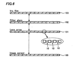
- An image sensor wafer 100 in which a plurality of image sensor chips 20 formed by wafer processing is disposed in a matrix form, is provided as shown in Fig. 6. Also, a lens array 101, which is a plurality of lenses 10 each having equivalent shape and size to the image sensor chip 20, is provided.
- an IR filter glass 102 in the same shape as the wafer is provided.
- an iris film 103 having the same shape as the wafer is also provided. Then the image sensor wafer 100, the lens array 101, the IR filter glass 102 and the iris film 103 are bonded together, forming an integrated structure.
- Fig. 7A is a plan view showing a first example of the lens array 101.
- the first example of the lens array 101 has a multitude of lenses 10 arranged to make an envelope of the array in a shape essentially same as the wafer, as shown in Fig. 7A.
- the lens array 101 is bonded to the image sensor wafer 100, as shown in Fig. 7B.
- Fig. 8A is a plan view showing a second example of the lens array 101.
- the second example of the lens array 101 is constructed using two types of sub-arrays, i.e., sub-array A and sub-array B, each nearly rectangular shaped, as shown in Fig. 8A.
- Four of the sub-array As and four of the sub-arrays B are bonded to the image sensor wafer 100, as shown in Fig. 8B.
- Fig. 9A is a plan view showing a third example of the lens array 101.
- the third example of the lens array 101 is constructed using only a single type of rectangular sub-array, as shown in Fig. 9A.
- the third example of the lens array 101 has an advantage of manufacturing simplicity, since it includes only one type of sub-array.
- the integrated structure described above is divided into individual camera modules 200 by cutting along borders between the image sensor chips with a dicing blade or a laser, as shown in Fig. 10.
- each of the individual camera modules 200 is mounted on a printed circuit board through bump electrodes 25A and 25B provided on a back surface of the image sensor chip 20.
- the manufacturing method described above corresponds to the structure shown in Fig. 2.
- the manufacturing method is adjusted to the structure shown in Fig. 3 by bonding the filter glass 102 between the image sensor wafer 100 and the lens array 101.
- the filter glass 102 is bonded after the image sensor wafer 100 and the lens array 101 are bonded together and the glass lens 45 is mounted above each of the lenses 10. The rest of the manufacturing process remains the same as described above.
- the iris film 103 is bonded after the image sensor wafer 100, the filter glass 102 and the lens array 101 are bonded together in this order and the glass lens 45 is mounted above each of the lenses 10. The rest of the manufacturing process remains the same as described above.
- the glass lens 45 may be mounted and bonded above the individual lens 10 after the image sensor wafer 100, the filter glass 102 and the lens array 101 are bonded together in this order and divided into individual camera modules 200.
- the invention provides a camera module for a portable device whose size is reduced to the size of the image sensor chip and is manufactured at a substantially reduced cost.
Landscapes
- Engineering & Computer Science (AREA)
- Multimedia (AREA)
- Signal Processing (AREA)
- Solid State Image Pick-Up Elements (AREA)
- Transforming Light Signals Into Electric Signals (AREA)
- Studio Devices (AREA)
- Lens Barrels (AREA)
Abstract
Description
Fig. 4 is a cross-sectional view showing the camera module according to the second embodiment of this invention. The same symbols are assigned to the same components in Fig. 4 as in Fig.2, and explanations of them are omitted.
Claims (17)
- A camera module comprising:an image sensor chip (20) comprising a semiconductor chip (21) having a photoelectronic transducer formed on a first portion of a front surface of the semiconductor chip (21) and having an electrode pad (23A, B) formed on a second portion of the front surface and connected to a terminal (25A, B) for external connection disposed on a back surface of the semiconductor chip (21); anda lens (10) bonded to the image sensor chip (20).
- The camera module of claim 1, wherein the image sensor ship (20) and the lens (10) substantially have a same size with respect to a primary plane thereof.
- The camera module of claim 1 or 2, further comprising a filter (30) to block light incident on the lens (10) at a predetermined range of wavelength.
- The camera module of claim 3, further comprising an iris portion (31) disposed on the filter (30) so as to provide an aperture for the light.
- The camera module of claim 1 or 2, further comprising a filter (30) disposed between the image sensor chip (20) and the lens (10).
- The camera module of claim 5, further comprising an iris portion (31) disposed on the lens (10) so as to provide an aperture for the light.
- The camera module according to any of claims 1 to 6, further comprising another lens (40) disposed above the lens (10) bonded to the image sensor chip (20).
- The camera module of claim 7, further comprising a positioning portion (43) positioning said another lens (40) at a predetermined distance from the lens (10) bonded to the image sensor chip (20).
- A method of manufacturing a camera module comprising:providing an image sensor wafer (100) comprising a plurality of image sensor chips (20), each of the image sensor chips comprising a photoelectronic transducer and a terminal for external connection;providing a lens array (101) comprising a plurality of lenses (10), each of the lenses (10) being configured to cover a corresponding image sensor chip (20);bonding the lens array (101) to a surface of the image sensor wafer (100) to form a bonded assembly; anddividing the bonded assembly into individual camera modules (200) so that each of the camera modules (200) comprises one of the image sensor chips (20) and one of the lenses (10).
- The method of claim 9, wherein a primary surface of the lens array (101) and a primary surface of the image sensor wafer (100) have substantially a same size.
- The method of claim 9, wherein the lens array (101) comprises a plurality of sub arrays.
- The method of claim 9, wherein the lens array (101) comprises a plurality of rectangular sub arrays.
- A method of manufacturing a camera module comprising:providing an image sensor wafer (100) comprising a plurality of image sensor chips (20), each of the image sensor chips comprising a photoelectronic transducer and a terminal for external connection;providing a lens array (101) comprising a plurality of lenses (10), each of the lenses being configured to cover a corresponding image sensor chip (20);providing a filter (102) and an iris portion (103);bonding the image sensor wafer (100), the lens array (101), the filter (102) and the iris portion (103) together to form a bonded assembly; anddividing the bonded assembly into individual camera modules (200) so that each of the camera modules (200) comprises one of the image sensor chips (20) and one of the lenses (10).
- A method of manufacturing a camera module comprising:providing an image sensor wafer (100) comprising a plurality of image sensor chips (20), each of the image sensor chips (20) comprising a photoelectronic transducer and a terminal for external connection;providing a lens array (101) comprising a plurality of lenses (10), each of the lenses (10) being configured to cover a corresponding image sensor chip (20);bonding the lens array (101) to a surface of the image sensor wafer (100) to form a bonded assembly;mounting an additional lens (40) over each of the lens (10); anddividing the bonded assembly into individual camera modules (200) so that each of the camera modules (200) comprises one of the image sensor chips (20) and one of the lenses (10, 40).
- The method of claim 14, wherein the additional lens (40) is mounted on the lens array (101) after the lens array (101) is bonded to the image sensor wafer (100).
- The method of claim 14, wherein the additional lens (40) is mounted on each of the individual camera modules (200) that are separated from each other.
- A camera module comprising:wherein a surface of the lens frame (12) is configure to serve as a barrel of the camera module.an image sensor chip (20) comprising a photoelectronic transducer; anda lens (10) bonded to the image sensor chip (20), the lens (10) comprising a lens body (11) and a lens frame (12),
Applications Claiming Priority (2)
| Application Number | Priority Date | Filing Date | Title |
|---|---|---|---|
| JP2002366274A JP2004200965A (en) | 2002-12-18 | 2002-12-18 | Camera module and manufacturing method thereof |
| JP2002366274 | 2002-12-18 |
Publications (2)
| Publication Number | Publication Date |
|---|---|
| EP1434426A2 true EP1434426A2 (en) | 2004-06-30 |
| EP1434426A3 EP1434426A3 (en) | 2004-11-10 |
Family
ID=32463469
Family Applications (1)
| Application Number | Title | Priority Date | Filing Date |
|---|---|---|---|
| EP03029192A Withdrawn EP1434426A3 (en) | 2002-12-18 | 2003-12-18 | Camera module and manufacturing method thereof |
Country Status (6)
| Country | Link |
|---|---|
| US (1) | US20040169763A1 (en) |
| EP (1) | EP1434426A3 (en) |
| JP (1) | JP2004200965A (en) |
| KR (1) | KR100577665B1 (en) |
| CN (1) | CN1510496A (en) |
| TW (1) | TWI236284B (en) |
Cited By (10)
| Publication number | Priority date | Publication date | Assignee | Title |
|---|---|---|---|---|
| DE102007007910A1 (en) * | 2007-02-14 | 2008-08-28 | Schott Ag | Camera module lens module/lens holder parallel production method, involves providing recesses with different inner dimensions, so that base of recesses with larger lateral dimensions form passages in passage holes |
| WO2009065759A1 (en) * | 2007-11-20 | 2009-05-28 | Continental Automotive Gmbh | Camera and production method for a camera |
| WO2009076788A1 (en) * | 2007-12-19 | 2009-06-25 | Heptagon Oy | Wafer stack, integrated optical device and method for fabricating the same |
| WO2009137022A1 (en) * | 2008-05-06 | 2009-11-12 | Tessera North America, Inc. | Camera system including radiation shield and method of shielding radiation |
| EP2136553A4 (en) * | 2007-04-17 | 2010-09-22 | Konica Minolta Opto Inc | METHOD FOR MANUFACTURING IMAGING DEVICE AND IMAGING DEVICE |
| US8092102B2 (en) | 2006-05-31 | 2012-01-10 | Flextronics Ap Llc | Camera module with premolded lens housing and method of manufacture |
| TWI392337B (en) * | 2005-10-11 | 2013-04-01 | 帝歐希數位光學有限公司 | Wafer-based camera module and manufacturing method thereof |
| US8477239B2 (en) | 2004-02-20 | 2013-07-02 | Digitaloptics Corporation | Integrated lens and chip assembly for a digital camera |
| US8488046B2 (en) | 2007-12-27 | 2013-07-16 | Digitaloptics Corporation | Configurable tele wide module |
| KR20140070532A (en) * | 2011-07-19 | 2014-06-10 | 헵타곤 마이크로 옵틱스 피티이. 리미티드 | Opto-electronic modules and methods of manufacturing the same |
Families Citing this family (32)
| Publication number | Priority date | Publication date | Assignee | Title |
|---|---|---|---|---|
| KR20060077519A (en) * | 2004-12-30 | 2006-07-05 | 삼성전자주식회사 | Camera lens unit of mobile terminal |
| KR20060087273A (en) | 2005-01-28 | 2006-08-02 | 삼성전기주식회사 | Semiconductor package and manufacturing method |
| KR100708940B1 (en) * | 2005-08-30 | 2007-04-17 | 삼성전기주식회사 | Infrared filter and window integrated camera module unit |
| CN100454070C (en) * | 2005-09-02 | 2009-01-21 | 亚洲光学股份有限公司 | Micro lens and manufacturing method thereof |
| KR100817060B1 (en) | 2006-09-22 | 2008-03-27 | 삼성전자주식회사 | Camera module and its manufacturing method |
| CN101632294B (en) | 2007-02-21 | 2012-08-22 | 柯尼卡美能达精密光学株式会社 | Imaging device and method for manufacturing the device |
| KR100855369B1 (en) * | 2007-03-19 | 2008-09-04 | 삼성전기주식회사 | Camera module |
| US7825985B2 (en) | 2007-07-19 | 2010-11-02 | Flextronics Ap, Llc | Camera module back-focal length adjustment method and ultra compact components packaging |
| US9118825B2 (en) | 2008-02-22 | 2015-08-25 | Nan Chang O-Film Optoelectronics Technology Ltd. | Attachment of wafer level optics |
| JP4930436B2 (en) * | 2008-04-03 | 2012-05-16 | コニカミノルタホールディングス株式会社 | Lens array sheet |
| KR20090108233A (en) * | 2008-04-11 | 2009-10-15 | 삼성전자주식회사 | Method for manufacturing a camera module, a camera module manufactured thereby, and an electronic system including the camera module |
| KR100927425B1 (en) * | 2008-05-09 | 2009-11-19 | 삼성전기주식회사 | Wafer Level Camera Module and Manufacturing Method Thereof |
| TW201033641A (en) * | 2008-09-18 | 2010-09-16 | Tessera North America Inc | Recessed optical surfaces |
| JP4768060B2 (en) * | 2008-09-25 | 2011-09-07 | シャープ株式会社 | Optical element, optical element wafer, optical element wafer module, optical element module, optical element module manufacturing method, electronic element wafer module, electronic element module manufacturing method, electronic element module, and electronic information device |
| JP4819152B2 (en) * | 2008-09-25 | 2011-11-24 | シャープ株式会社 | Optical element wafer, optical element wafer module, optical element module, method for manufacturing optical element module, electronic element wafer module, method for manufacturing electronic element module, electronic element module, and electronic information device |
| JP4764942B2 (en) * | 2008-09-25 | 2011-09-07 | シャープ株式会社 | Optical element, optical element wafer, optical element wafer module, optical element module, optical element module manufacturing method, electronic element wafer module, electronic element module manufacturing method, electronic element module, and electronic information device |
| JP4764941B2 (en) * | 2008-09-25 | 2011-09-07 | シャープ株式会社 | Optical element, optical element wafer, optical element wafer module, optical element module, optical element module manufacturing method, electronic element wafer module, electronic element module manufacturing method, electronic element module, and electronic information device |
| EP2333599A4 (en) | 2008-10-01 | 2012-03-14 | Konica Minolta Holdings Inc | IMAGING UNIT AND IMAGING DEVICE |
| JP5596293B2 (en) * | 2009-03-03 | 2014-09-24 | オリンパス株式会社 | Imaging unit |
| US20100238346A1 (en) * | 2009-03-17 | 2010-09-23 | Hong Kong Applied Science And Technology Research Institute Co. Ltd. | Compact imaging device |
| JP2010243695A (en) * | 2009-04-03 | 2010-10-28 | Konica Minolta Opto Inc | Actuator, drive device, and imaging device |
| CN101872049B (en) * | 2009-04-27 | 2014-10-15 | 鸿富锦精密工业(深圳)有限公司 | Lens structure and manufacturing method thereof |
| US9419032B2 (en) | 2009-08-14 | 2016-08-16 | Nanchang O-Film Optoelectronics Technology Ltd | Wafer level camera module with molded housing and method of manufacturing |
| US8193599B2 (en) * | 2009-09-02 | 2012-06-05 | Himax Semiconductor, Inc. | Fabricating method and structure of a wafer level module |
| JP5445030B2 (en) * | 2009-10-27 | 2014-03-19 | 凸版印刷株式会社 | Camera module and manufacturing method thereof |
| US8564896B2 (en) | 2010-08-20 | 2013-10-22 | Hong Kong Applied Science And Technology Research Institute Co., Ltd. | Compact imaging device |
| WO2012161802A2 (en) | 2011-02-24 | 2012-11-29 | Flextronics Ap, Llc | Autofocus camera module packaging with circuitry-integrated actuator system |
| CN103402049A (en) * | 2013-07-28 | 2013-11-20 | 宁波远大成立科技股份有限公司 | Image sensing element and manufacturing method |
| CN106961537A (en) * | 2016-01-08 | 2017-07-18 | 华天科技(昆山)电子有限公司 | Array camera module structure and its manufacture method |
| KR102178971B1 (en) * | 2019-08-30 | 2020-11-13 | 한국광기술원 | Laser Dicing Apparatus and Method for Dicing Wafer Lens Array |
| CN114740582A (en) * | 2022-04-15 | 2022-07-12 | 华天慧创科技(西安)有限公司 | Lens module, manufacturing method thereof and camera |
| US20240201466A1 (en) * | 2022-12-20 | 2024-06-20 | Meta Platforms Technologies, Llc | Barrel-less compact camera device with micromolding lens stack |
Family Cites Families (16)
| Publication number | Priority date | Publication date | Assignee | Title |
|---|---|---|---|---|
| JP2950714B2 (en) * | 1993-09-28 | 1999-09-20 | シャープ株式会社 | Solid-state imaging device and method of manufacturing the same |
| KR970705294A (en) * | 1995-05-31 | 1997-09-06 | 이데이 노부유키 | Image pickup apparatus, image pickup adapter apparatus, signal processing apparatus, signal processing method, information processing apparatus, and information processing method Processing Apparatus, and Information Processing Method) |
| US6795120B2 (en) * | 1996-05-17 | 2004-09-21 | Sony Corporation | Solid-state imaging apparatus and camera using the same |
| US6217796B1 (en) * | 1998-11-17 | 2001-04-17 | Nisshinbo Industries, Inc. | Near infrared absorption composition |
| WO2000040010A1 (en) * | 1998-12-24 | 2000-07-06 | Photobit Corporation | Contoured surface cover plate for image sensor array |
| JP3360655B2 (en) * | 1999-07-08 | 2002-12-24 | 日本電気株式会社 | Semiconductor device |
| JP3651577B2 (en) * | 2000-02-23 | 2005-05-25 | 三菱電機株式会社 | Imaging device |
| JP2001245217A (en) * | 2000-03-02 | 2001-09-07 | Olympus Optical Co Ltd | Small imaging module |
| JP3463294B2 (en) * | 2000-03-27 | 2003-11-05 | 株式会社リコー | Optical scanning device |
| JP3607160B2 (en) * | 2000-04-07 | 2005-01-05 | 三菱電機株式会社 | Imaging device |
| EP1180718A1 (en) * | 2000-08-11 | 2002-02-20 | EM Microelectronic-Marin SA | Apparatus for taking images of small dimensions, particularly still or motion picture camera |
| JP2002231918A (en) * | 2001-02-06 | 2002-08-16 | Olympus Optical Co Ltd | Solid-state imaging device and manufacturing method thereof |
| JP2002252797A (en) * | 2001-02-26 | 2002-09-06 | Sony Corp | Solid-state imaging device |
| US20040012698A1 (en) * | 2001-03-05 | 2004-01-22 | Yasuo Suda | Image pickup model and image pickup device |
| US6635941B2 (en) * | 2001-03-21 | 2003-10-21 | Canon Kabushiki Kaisha | Structure of semiconductor device with improved reliability |
| JP2002290842A (en) * | 2001-03-23 | 2002-10-04 | Sanyo Electric Co Ltd | Method for manufacturing solid-state imaging device |
-
2002
- 2002-12-18 JP JP2002366274A patent/JP2004200965A/en active Pending
-
2003
- 2003-12-10 TW TW092134812A patent/TWI236284B/en not_active IP Right Cessation
- 2003-12-17 US US10/736,777 patent/US20040169763A1/en not_active Abandoned
- 2003-12-17 KR KR1020030092239A patent/KR100577665B1/en not_active Expired - Fee Related
- 2003-12-18 EP EP03029192A patent/EP1434426A3/en not_active Withdrawn
- 2003-12-18 CN CNA2003101147289A patent/CN1510496A/en active Pending
Cited By (15)
| Publication number | Priority date | Publication date | Assignee | Title |
|---|---|---|---|---|
| US8477239B2 (en) | 2004-02-20 | 2013-07-02 | Digitaloptics Corporation | Integrated lens and chip assembly for a digital camera |
| TWI392337B (en) * | 2005-10-11 | 2013-04-01 | 帝歐希數位光學有限公司 | Wafer-based camera module and manufacturing method thereof |
| US8092102B2 (en) | 2006-05-31 | 2012-01-10 | Flextronics Ap Llc | Camera module with premolded lens housing and method of manufacture |
| DE102007007910A1 (en) * | 2007-02-14 | 2008-08-28 | Schott Ag | Camera module lens module/lens holder parallel production method, involves providing recesses with different inner dimensions, so that base of recesses with larger lateral dimensions form passages in passage holes |
| US8339502B2 (en) | 2007-04-17 | 2012-12-25 | Konica Minolta Opto, Inc. | Imaging device manufacturing method and imaging device |
| EP2136553A4 (en) * | 2007-04-17 | 2010-09-22 | Konica Minolta Opto Inc | METHOD FOR MANUFACTURING IMAGING DEVICE AND IMAGING DEVICE |
| DE102007055322B4 (en) * | 2007-11-20 | 2012-09-06 | Continental Automotive Gmbh | Manufacturing process for a camera |
| DE102007055322A1 (en) * | 2007-11-20 | 2009-06-04 | Continental Automotive Gmbh | Camera and manufacturing process for a camera |
| WO2009065759A1 (en) * | 2007-11-20 | 2009-05-28 | Continental Automotive Gmbh | Camera and production method for a camera |
| US8580600B2 (en) | 2007-11-20 | 2013-11-12 | Continental Automotive Gmbh | Camera and production method for a camera |
| US8289635B2 (en) | 2007-12-19 | 2012-10-16 | Heptagon Micro Optics Pte. Ltd. | Wafer stack, integrated optical device and method for fabricating the same |
| WO2009076788A1 (en) * | 2007-12-19 | 2009-06-25 | Heptagon Oy | Wafer stack, integrated optical device and method for fabricating the same |
| US8488046B2 (en) | 2007-12-27 | 2013-07-16 | Digitaloptics Corporation | Configurable tele wide module |
| WO2009137022A1 (en) * | 2008-05-06 | 2009-11-12 | Tessera North America, Inc. | Camera system including radiation shield and method of shielding radiation |
| KR20140070532A (en) * | 2011-07-19 | 2014-06-10 | 헵타곤 마이크로 옵틱스 피티이. 리미티드 | Opto-electronic modules and methods of manufacturing the same |
Also Published As
| Publication number | Publication date |
|---|---|
| CN1510496A (en) | 2004-07-07 |
| JP2004200965A (en) | 2004-07-15 |
| TWI236284B (en) | 2005-07-11 |
| EP1434426A3 (en) | 2004-11-10 |
| TW200421862A (en) | 2004-10-16 |
| US20040169763A1 (en) | 2004-09-02 |
| KR100577665B1 (en) | 2006-05-10 |
| KR20040054525A (en) | 2004-06-25 |
Similar Documents
| Publication | Publication Date | Title |
|---|---|---|
| US20040169763A1 (en) | Camera module and manufacturing method thereof | |
| EP1443754A2 (en) | Camera module and manufacturing method thereof | |
| US6853005B2 (en) | Camera module and manufacturing method thereof | |
| US7948555B2 (en) | Camera module and electronic apparatus having the same | |
| US7166907B2 (en) | Image sensor module with substrate and frame and method of making the same | |
| JP4310348B2 (en) | Solid-state imaging device and electronic apparatus including the same | |
| CN101652695B (en) | Wafer level camera module and method of manufacture | |
| US20070126912A1 (en) | Camera module and manufacturing method for such a camera module | |
| CN101632294B (en) | Imaging device and method for manufacturing the device | |
| US20050116138A1 (en) | Method of manufacturing a solid state image sensing device | |
| JP5035707B2 (en) | Imaging device manufacturing method and imaging device | |
| KR100824812B1 (en) | Compact camera module and manufacturing method thereof | |
| JP3993532B2 (en) | Method for manufacturing enclosed optical sensor and enclosed optical sensor manufactured by the method | |
| EP1432239A1 (en) | Camera module | |
| JP2004229167A (en) | Manufacturing method of camera module | |
| EP1603166A1 (en) | Image pickup device and camera module | |
| JP2005317745A (en) | Solid-state imaging device and manufacturing method thereof | |
| US20240388781A1 (en) | Imaging unit and imaging device | |
| US20030146998A1 (en) | Small-size imaging apparatus, in particular photographic appliance or camera | |
| US9111827B2 (en) | Manufacturing method of solid-state imaging apparatus, solid-state imaging apparatus, and electronic imaging apparatus | |
| JP2004233482A (en) | Method of manufacturing camera module | |
| CN103081105A (en) | Image pickup device, image pickup module and camera | |
| KR20240051114A (en) | Semiconductor devices and electronic devices | |
| JP2004233483A (en) | The camera module | |
| JP3959711B2 (en) | Solid-state imaging device and manufacturing method thereof |
Legal Events
| Date | Code | Title | Description |
|---|---|---|---|
| PUAI | Public reference made under article 153(3) epc to a published international application that has entered the european phase |
Free format text: ORIGINAL CODE: 0009012 |
|
| AK | Designated contracting states |
Kind code of ref document: A2 Designated state(s): AT BE BG CH CY CZ DE DK EE ES FI FR GB GR HU IE IT LI LU MC NL PT RO SE SI SK TR |
|
| AX | Request for extension of the european patent |
Extension state: AL LT LV MK |
|
| PUAL | Search report despatched |
Free format text: ORIGINAL CODE: 0009013 |
|
| AK | Designated contracting states |
Kind code of ref document: A3 Designated state(s): AT BE BG CH CY CZ DE DK EE ES FI FR GB GR HU IE IT LI LU MC NL PT RO SE SI SK TR |
|
| AX | Request for extension of the european patent |
Extension state: AL LT LV MK |
|
| 17P | Request for examination filed |
Effective date: 20050309 |
|
| AKX | Designation fees paid |
Designated state(s): DE FI FR GB |
|
| 17Q | First examination report despatched |
Effective date: 20080226 |
|
| STAA | Information on the status of an ep patent application or granted ep patent |
Free format text: STATUS: THE APPLICATION IS DEEMED TO BE WITHDRAWN |
|
| 18D | Application deemed to be withdrawn |
Effective date: 20080909 |