EP1434342A2 - Pulse width modulation signal generating apparatus having two dead times for on-timings - Google Patents
Pulse width modulation signal generating apparatus having two dead times for on-timings Download PDFInfo
- Publication number
- EP1434342A2 EP1434342A2 EP03090440A EP03090440A EP1434342A2 EP 1434342 A2 EP1434342 A2 EP 1434342A2 EP 03090440 A EP03090440 A EP 03090440A EP 03090440 A EP03090440 A EP 03090440A EP 1434342 A2 EP1434342 A2 EP 1434342A2
- Authority
- EP
- European Patent Office
- Prior art keywords
- signal
- circuit
- signals
- count value
- coincidence
- Prior art date
- Legal status (The legal status is an assumption and is not a legal conclusion. Google has not performed a legal analysis and makes no representation as to the accuracy of the status listed.)
- Withdrawn
Links
Images






Classifications
-
- H—ELECTRICITY
- H02—GENERATION; CONVERSION OR DISTRIBUTION OF ELECTRIC POWER
- H02M—APPARATUS FOR CONVERSION BETWEEN AC AND AC, BETWEEN AC AND DC, OR BETWEEN DC AND DC, AND FOR USE WITH MAINS OR SIMILAR POWER SUPPLY SYSTEMS; CONVERSION OF DC OR AC INPUT POWER INTO SURGE OUTPUT POWER; CONTROL OR REGULATION THEREOF
- H02M1/00—Details of apparatus for conversion
- H02M1/38—Means for preventing simultaneous conduction of switches
-
- H—ELECTRICITY
- H02—GENERATION; CONVERSION OR DISTRIBUTION OF ELECTRIC POWER
- H02M—APPARATUS FOR CONVERSION BETWEEN AC AND AC, BETWEEN AC AND DC, OR BETWEEN DC AND DC, AND FOR USE WITH MAINS OR SIMILAR POWER SUPPLY SYSTEMS; CONVERSION OF DC OR AC INPUT POWER INTO SURGE OUTPUT POWER; CONTROL OR REGULATION THEREOF
- H02M7/00—Conversion of AC power input into DC power output; Conversion of DC power input into AC power output
- H02M7/42—Conversion of DC power input into AC power output without possibility of reversal
- H02M7/44—Conversion of DC power input into AC power output without possibility of reversal by static converters
- H02M7/48—Conversion of DC power input into AC power output without possibility of reversal by static converters using discharge tubes with control electrode or semiconductor devices with control electrode
- H02M7/53—Conversion of DC power input into AC power output without possibility of reversal by static converters using discharge tubes with control electrode or semiconductor devices with control electrode using devices of a triode or transistor type requiring continuous application of a control signal
- H02M7/537—Conversion of DC power input into AC power output without possibility of reversal by static converters using discharge tubes with control electrode or semiconductor devices with control electrode using devices of a triode or transistor type requiring continuous application of a control signal using semiconductor devices only, e.g. single switched pulse inverters
- H02M7/539—Conversion of DC power input into AC power output without possibility of reversal by static converters using discharge tubes with control electrode or semiconductor devices with control electrode using devices of a triode or transistor type requiring continuous application of a control signal using semiconductor devices only, e.g. single switched pulse inverters with automatic control of output wave form or frequency
- H02M7/5395—Conversion of DC power input into AC power output without possibility of reversal by static converters using discharge tubes with control electrode or semiconductor devices with control electrode using devices of a triode or transistor type requiring continuous application of a control signal using semiconductor devices only, e.g. single switched pulse inverters with automatic control of output wave form or frequency by pulse-width modulation
Definitions
- the invention relates to a pulse width modulation (PWM) signal generating apparatus for generating PWM signals for controlling a PWM inverter for driving a motor.
- PWM pulse width modulation
- a PWM signal generating apparatus generates PWM signals for controlling the PWM inverter.
- a three-phase PWM inverter is constructed by three arms, i.e., a U-phase arm, a V-phase arm and a W-phase arm, each of the arms including an upper side power transistor and a lower side power transistor connected in series between two DC power lines.
- a three-phase PWM signal generating apparatus generates complementary U-phase and /U-phase PWM signals, complementary V-phase and /V-phase PWM signals, and complementary W-phase and /W-phase PWM signals.
- the power transistors of the U-phase arm carry out a complementary push-pull operation using the U-phase and /U-phase signals.
- the power transistors of the V-phase arm carry out a complementary push-pull operation using the V-phase and /V-phase signals.
- the power transistors of the W-phase arm carry out a complementary push-pull operation using the W-phase and /W-phase signals.
- a common dead time is introduced to delay the ON-timing of each of the U-phase PWM signal, the /U-phase PWM signal, the V-phase PWM signal, the /V-phase PWM signal, the W-phase PWM signal and the /W-phase PWM signal, so that the ON-timing of each of the power transistors of the three-phase PWM inverter is delayed (see: JP-A-10-112982).
- a first dead time is introduced into the ON timing of one of the two complementary PWM signals, and a second dead time is introduced into the ON timing of the other.
- the first and second dead times are individually set. Therefore, the first dead time is optimum for controlling an upper side power transistor of a PWM inverter, and the second dead time is optimum for controlling a lower side power transistor of the PWM inverter.
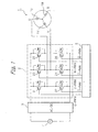
- reference numeral 1 designates a stator of the AC motor having a U-phase winding 1U, a V-phase winding 1V and a W-phase winding 1W.
- the stator 1 is associated with a rotor (not shown).
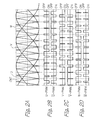
- a three-phase PWM inverter 2 receives a DC voltage from an AC/DC converter 3 powered by an AC power supply source 4, and inverts the DC voltage into three-phase AC voltages U, V and W as shown in Fig. 2A which are applied to the windings 1U, 1V and 1W of the stator 1.
- Inverter 2 is a serial-parallel bridge circuit having a U-phase arm, a V-phase arm and W-phase arm.
- the U-phase arm for generating the AC voltage U is constructed by a series of an upper side PNP-type bipolar power transistor 21 and a lower side PNP-type bipolar power transistor 22 associated with counterelectromotive force regenerative diodes 21a and 22a connected in parallel thereto.
- the V-phase arm for generating the AC voltage V is constructed by a series of an upper side PNP-type bipolar power transistor 23 and a lower side PNP-type bipolar power transistor 24 associated with counterelectromotive force regenerative diodes 23 a and 24a connected in parallel thereto.
- the W-phase arm for generating the AC voltage W is constructed by a series of an upper side PNP-type bipolar power transistor 25 and a lower side PNP-type bipolar power transistor 26 associated with counterelectromotive force regenerative diodes 25a and 26a connected in parallel thereto.
- Inverter 2 is controlled by a three-phase PWM signal generating apparatus 5 which generates complementary U-phase and /U-phase PWM signals as shown in Fig. 2B, complementary V-phase and /V-phase PWM signals as shown in Fig. 2C, and complementary W-phase and /W-phase PWM signals as shown in Fig. 2D.
- the power transistors 21 and 22 carry out a push-pull operation using the U- and /U-phase PWM signals.
- the power transistors 23 and 24 carry out a push-pull operation using the V- and /V-phase PWM signals.
- the power transistors 25 and 26 carry out a push-pull operation using the W- and /W-phase PWM signals.
- the stator 1 is driven by the three-phase AC voltages U, V and W.
- a value CNT of a triangular carrier signal is generated within the apparatus 5 of Fig. 1 in order to generate the U- and /U- phase PWM signals, the V- and /V- phase PWM signals and the W- and /W- phase PWM signals.
- a short-circuit current may flow therethrough.
- the ON time period of the U-phase PWM signal is never superposed onto the ON time period of the /U-phase PWM signal
- the ON time period of the V-phase PWM signal is never superposed onto the ON time period of the /V-phase PWM signal
- the ON time period of the W-phase PWM signal is never superposed onto the ON time period of the /W-phase PWM signal.
- a dead time d0 is introduced into the ON timings of the U-phase PWM signal, the V-phase PWM signal, and the W-phase PWM signal
- a dead time d1 is introduced into the ON timings of the /U-phase PWM signal, the /V-phase PWM signal, and the /W-phase PWM signal. This will be explained in detail below.
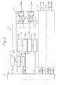
- a U-phase PWM signal generating section 11U, a V-phase PWM signal generating section 11V and a W-phase PWM signal generating section 11 W which have the same configuration are provided, and a control circuit 12 for controlling the entire of the apparatus of Fig. 3 are provided.
- the control circuit 12 may be constructed by a microcomputer.
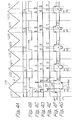
- an up/down counter 101 receives a clock signal CLK to generate a value CNT of a triangular carrier signal as shown in Fig. 4A, and a count direction signal U/D as shown in Fig. 4B.
- the period of the triangular carrier signal is one twelfth of the period of the three-phase AC voltages U, V and W.
- the triangular carrier signal and the counting direction signal U/D are supplied to the U-phase PWM signal generating section 11U, the V-phase PWM signal generating section 11V and the W-phase PWM signal generating section 11 W. Also, the counting direction signal U/D is supplied as an interrupt signal to the control circuit 12.
- a comparator 102 compares the value CNT of the triangular carrier signal with a reference value CNTU stored in a compare register 103. As a result, when the value CNT of the triangular carrier signal coincides with the reference value CNTU of the compare register 103, the comparator 102 generates a coincidence signal S1 as shown in Fig. 4C.
- the coincidence signal S1 is supplied as set signals to delay circuits 104 and 105 which are constructed by down counters. Therefore, dead times d1 and d2 stored in dead time registers 104a and 105a, respectively, are set in the delay circuits 104 and 105, respectively, so that the delay circuits 104 and 105 serving as the down counters are counted down.
- the delay circuit 104 when the dead time d1 has passed, the delay circuit 104 generates a delayed coincidence signal S2 as shown in Fig. 4D.
- the delay circuit 105 generates a delayed coincidence signal S3 as shown in Fig. 4E.
- the coincidence signal S1 and the delayed coincidence signals S2 and S3 are supplied to a selection circuit 107 formed by four gate circuits G1, G2, G3 and G4 controlled by the counting direction signal U/D to operate RS-type flip-flops 108 and 109.
- the gate circuits G1 and G4 are activated by the counting direction signal U/D. Therefore, the delayed coincidence signal S2 passes through the gate circuit G1 to reset flip-flop 108, so that the U-phase PWM signal is made "0" (ON level) as shown in Fig. 4F. Also, the coincidence signal S3 passes through the gate circuit G4 to set flip-flop 109, so that the /U-phase PWM signal is made "1" (OFF level) as shown in Fig. 4G.
- the gate circuits G2 and G3 are activated by the counting direction signal U/D. Therefore, the coincidence signal S1 passes through the gate circuit G2 to set flip-flop 108, so that the U-phase PWM signal is made "1" (OFF level) as shown in Fig. 4F. Also, the delayed coincidence signal S3 passes through the gate circuit G3 to set flip-flop 109, so that the /U-phase PWM signal is made "0" (ON level) as shown in Fig. 4G.
- the ON timing of the U-phase PWM signal is delayed by the dead time d1
- the ON timing of the /U-phase PWM signal is delayed by the dead time d2.
- the dead times d1 and d2 of the dead time registers 104a and 105a for the U-phase PWM signal generating section 11U as well as the dead times d3 and d4 for the V-phase PWM signal generating section 11V and the dead times d5 and d6 for the W-phase PWM signal generating section 11W are set by the control circuit 12 in advance.
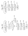
- the reference value CNTU of the compare register 103 as well as the reference value CNTV of the compare registers (not shown) for the V-phase PWM signal generating section 11V and the reference value CNTW of the compare registers (not shown) for the W-phase PWM signal generating section 11W are set by interrupt routines as illustrated in Figs. 5A and 5B.
- the interrupt routine of Fig. 5A is started every time the counting direction signal U/D is switched from "1" (down counting state) to "0" (up counting state).
- a value i is counted up by +1.
- step 502 it is determined whether or not i > 11 is satisfied.
- the U-phase PWM signal, the V-phase PWM signal and the W-phase PWM signal have a period of 12 PWM pulses. Only when i > 11, does the control proceed to step 503 which clears the value i, i.e., i ⁇ 0. Otherwise, the control proceeds directly to step 504.
- the reference value CNTU is set in the compare register 103.
- the reference value CNTV is set in the compare register of the V-phase PWM signal generating section 11V.
- the reference value CNTW is set in the compare register of the W-phase PWM signal generating section 41W.
- the reference values U u (0), U u (1), ..., U u (11); V u (0), V u (1), ..., V u (11); and W u (0), W u (1), ..., W u (11) are predetermined in accordance with the abilities of the power transistors 21, 22, 23, 24, 25 and 26, and are stored in a read-only memory (ROM) of the control circuit 12.
- the interrupt routine of Fig. 5B is started every time the counting direction signal U/D is switched from "0" (up counting state) to "1" (down counting state).
- the reference value CNTU is set in the compare register 103.
- the reference value CNTV is set in the compare register of the V-phase PWM signal generating section 11V.
- the reference value CNTW is set in the compare register of the W-phase PWM signal generating section 11W.
- the reference values U d (0), U d (1), ..., U d (11); V d (0), V d (1), ..., V d (11); and W d (0), W d (1), ..., W d (11) are also predetermined in accordance with the abilities of the power transistors 21, 22, 23, 24, 25 and 26, and are stored in the ROM of the control circuit 12.
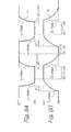
- an optimum complementary push-pull operation time is increased. That is, if the driving ability of the upper side power transistor 21 is larger than that of the lower side power transistor 22, the ON/OFF operation state of transistor 21 is changed in accordance with the U-phase PWM signal as shown in Fig. 6A, and the ON/OFF operation state of transistor 22 is changed in accordance with the /U-phase PWM signal as shown in Fig. 6B.
- an ON switching time ⁇ 1 of transistor 21 is smaller than an ON switching time ⁇ 3 of transistor 22.
- an OFF switching time ⁇ 2 of transistor 21 is smaller than an OFF switching time ⁇ 4 of transistor 22.
- T2 is a time period where transistor 21 is completely turned OFF and transistor 22 is completely turned ON.
- the optimum complementary push-pull operation time can be increased, which would increase the total torque of the motor, thus decreasing the power consumption.
- the motor can be rotated by its inertia during a dead time. Therefore, the smaller the dead time, the smoother the inverter output voltage. That is, if the dead time d0 is relatively large as in the prior art, the inverter output voltage such as the U-phase voltage is not smooth as shown in Fig. 9A.
- the dead time d0 is relatively large as in the prior art, the inverter output voltage such as the U-phase voltage is not smooth as shown in Fig. 9A.
- Figs. 8A and 8B although d2 > d0 > d1, if the dead time d2 is brought close to d0 to sacrifice the optimum complementary push-pull operation time period, the average dead time is relatively small, so that the inverter output voltage such as the U-phase voltage is smooth as shown in Fig. 9B.
- the U-phase PWM signal generating section 11U, the V-phase PWM signal generating section 11V and the W-phase PWM signal generating section 11W of Fig. 3 are replaced by a U-phase PWM signal generating section 21U, a V-phase PWM signal generating section 21 V and a W-phase PWM signal generating section 21 W, respectively.
- gate circuits 201 and 202 and an OR circuit 203 are added to the elements of the U-phase PWM signal generating circuit 11U of Fig. 3. That is, the gate circuit 201 controlled by the counting direction signal U/D is connected between the comparator 102 and the delay circuit 104, and the gate circuit 202 controlled by the counting direction signal U/D is connected between the comparator 102 and the delay circuit 105.
- delayed coincidence signals S2 and S3 are combined by the OR circuit 203 to generate a delayed coincidence signal S4.
- gate circuits and an OR circuit corresponding to the gate circuits 201 and 202 and the OR circuit 203 are provided in section 21 V and section 21W.
- the signals of the apparatus of Fig. 10 are shown in Figs. 11A through 11H. That is, when the counting direction signal U/D is "1", the coincidence signal S1 of the comparator 101 passes through the gate circuit 201 to reach the delay circuit 104, thus generating the delayed coincidence signal S2 as shown in Fig. 11D. On the other hand, when the counting direction signal U/D is "0", the coincidence signal S1 of the comparator 101 passes through the gate circuit 202 to reach the delay circuit 105, thus generating the delayed coincidence signal S3 as shown in Fig. 11E. Even in this case, the same U-phase PWM signal and the same /U-phase PWM signal can be obtained as shown in Figs. 11G and 11 H.
- the power consumption can be decreased, and the noise can be decreased, as compared with the first embodiment.
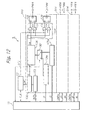
- the U-phase PWM signal generating section 21U, the V-phase PWM signal generating section 21V and the W-phase PWM signal generating section 21W of Fig. 10 are replaced by a U-phase PWM signal generating section 31U, a V-phase PWM signal generating section 31V and a W-phase PWM signal generating section 31W, respectively.
- section 31U the gate circuits 201 and 202 of Fig. 10 are replaced by a selection circuit 301, and the delay circuit 105 and the OR circuit 106 of Fig. 10 are deleted.
- the signals of the apparatus of Fig. 12 are shown in Figs. 13A through 13H. That is, when the counting direction signal U/D is "1", the switch circuit 301 selects the dead time d1 of the dead time register 104a, thus generating the delayed signal S4 by the dead time d1 as shown in Fig. 13D. On the other hand, when the counting direction signal U/D is "0", the dead time d2 of the dead time register 105a is selected, thus generating the delayed signal S4 by the dead time d2 as shown in Fig. 13D. Even in this case, the same U-phase PWM signal and the same /U-phase PWM signal can be obtained as shown in Figs. 13E and 13F.
- both of the delay circuits 104 and 105 are provided.
- only the delay circuit 104 is provided.
- the manufacturing cost can be decreased as compared with the first embodiment.
- the U-phase PWM signal generating section 11U, the V-phase PWM signal generating section 11V, the W-phase PWM signal generating section 11W and the control circuit 12 of Fig. 3 are replaced by a U-phase PWM signal generating section 41U, a V-phase PWM signal generating section 41 V, a W-phase PWM signal generating section 41W and a control circuit 42, respectively.
- section 41U the delay circuits 104 and 105, the dead time registers 104a and 105a and the OR circuit 106 of Fig. 3 are deleted, and a comparator 102' and a compare register 103' are added to the elements of the U-phase PWM signal generating section 11U of Fig. 3.
- the comparator 102 compares the value CNT of the triangular carrier signal with a reference value CNTU stored in the compare register 103. As a result, when the value CNT of the triangular carrier signal coincides with the reference value CNTU of the compare register 103, the comparator 102 generates a coincidence signal S1 as shown in Fig. 15C.
- the coincidence signal S1 is supplied as a set signal and a reset signal via the gate circuits G1 and G2 of the selection circuit 107 to the RS-type flip-flop 108.
- the gate circuit G2 is activated by the counting direction signal U/D. Therefore, the signal S1 passes through the gate circuit G2 to set the RS-type flip-flop 108, so that the U-phase PWM signal is made "1" (OFF level) as shown in Fig. 15E.
- the gate circuit G1 is activated by the counting direction signal U/D. Therefore, the signal S1 passes through the gate circuit G1 to reset the RS-type flip-flop 108, so that the U-phase PWM signal is made "0" (ON level) as shown in Fig. 15E.
- the comparator 102' compares the value CNT of the triangular carrier signal with a reference value CNTU' stored in the compare register 103'. As a result, when the value CNT of the triangular carrier signal coincides with the reference value CNTU' of the compare register 103', the comparator 102' generates a coincidence signal S1' as shown in Fig. 15D.
- the coincidence signal S1' is supplied as a set signal and a reset signal via the gate circuits G3 and G4 of the selection circuit 107 to the RS-type flip-flop 109.
- the gate circuit G3 is activated by the counting direction signal U/D. Therefore, the signal S1' passes through the gate circuit G3 to reset flip-flop 109, so that the /U-phase PWM signal is made "0" (ON level) as shown in Fig. 15F.
- the gate circuit G4 is activated by the counting direction signal U/D. Therefore, the signal S1' passes through the gate circuit G4 to set flip-flop 109, so that the /U-phase PWM signal is made "1" (OFF level) as shown in Fig. 15F.
- the ON timing of the /U-phase PWM signal can be assumed to be delayed by the dead time d2.
- the reference values CNTU and CNTU' of the compare registers 103 and 103' as well as the reference values CNTV and CNTV' of the compare registers (not shown) for section 41V and the reference values CNTW and CNTW' of the compare registers (not shown) for section 41W are set by interrupt routines as illustrated in Figs. 16A and 16B.
- the interrupt routine of Fig. 16A is started every time the counting direction signal U/D is switched from "1" (down counting state) to "0" (up counting state).
- a value i is counted up by +1.
- step 1602 it is determined whether or not i > 11 is satisfied. Only when i > 11, does the control proceed to step 1603 which clears the value i, i.e., i ⁇ 0. Otherwise, the control proceeds directly to step 1604.
- the reference value CNTU is set in the compare register 103.
- the reference value CNTU' is set in the compare register 103'.
- the reference value CNTV is set in the compare register of the V-phase PWM signal generating section 41V.
- the reference value CNTV' is set in the compare register of the V-phase PWM signal generating section 41V.
- the reference value CNTW is set in the compare register of the W-phase PWM signal generating section 41W.
- the reference value CNTW' is set in the compare register of the W-phase PWM signal generating section 41W.
- the reference values U u (0), U u (1), ..., U u (11); U' u (0), U' u (1), ..., U' u (11); V u (0), V u (1), ..., V u (11); V' u (0), V' u (1), ..., V' u (11); W u (0), W u (1), ..., W u (11); and W' u (0), W' u (1), ..., W' u (11) are predetermined in accordance with the abilities of transistors 21, 22, 23, 24, 25 and 26, and are stored in a ROM of the control circuit 42.
- the interrupt routine of Fig. 16B is started every time the counting direction signal U/D is switched from "0" (up counting state) to "1" (down counting state).
- the reference value CNTU is set in the compare register 103.
- the reference value CNTU' is set in the compare register 103'.
- the reference value CNTV is set in the compare register of the V-phase PWM signal generating section 41V.
- the reference value CNTV' is set in the compare register of the V-phase PWM signal generating section 41 V.
- the reference value CNTW is set in the compare register of the W-phase PWM signal generating section 11W.
- the reference value CNTW' is set in the compare register of the W-phase PWM signal generating section 11 W.
- the reference values U d (0), U d (1), ..., U d (11); U' d (0), U' d (1), ..., U' d (11); V d (0), V d (1), ..., V d (11); V' d (0), V' d (1), ..., V' d (11); W d (0), W d (1), ..., W d (11); and W' d (0), W' d (1), ..., W' d (11) are also predetermined in accordance with the abilities of the power transistors 21, 22, 23, 24, 25 and 26, and are stored in the ROM of the control circuit 42.
- the manufacturing cost can be decreased.
- section 11U, section 11V, section 11W and circuit 12 of Fig. 3 are replaced by a U-phase PWM signal generating section 51U, a V-phase PWM signal generating section 51 V, a W-phase PWM signal generating section 51W and a control circuit 52, respectively.
- Up/down counters 101A, 101B and 101C are provided instead of the up/down counter 101 of Fig. 3.
- An initial value 0000 H is set by the control circuit 52 in the up/down counter 101A
- a dead time d2 is set by the control circuit 52 in the up/down counter 101B
- a dead time (d + d2) is set by the control circuit 52 in the up/down counter 101C.
- the counting direction U/D of the up/down counters 101A, 101B and 101C are controlled by the control circuit 52, so that the up/down counters 101A, 101B and 101C generate triangular carrier signals whose values are CNTA, CNTB and CNTC, respectively, as shown in Fig. 18A, in synchronization with a counting direction signal U/D as shown in Fig. 18B.
- section 51U the delay circuits 104 and 105, the dead time registers 104a and 105a and the OR circuit 106 of Fig. 3 are deleted, and comparators 501A, 501B and 501C and a compare register 502 are provided instead of the comparator 102 and the compare register 103 of Fig. 3.
- the comparator 501A compares the value CNTA of the triangular carrier signal of the up/down counter 101A with a reference value CNTU stored in register 502. As a result, when the value CNTA of the triangular carrier signal of the up/down counter 101A coincides with the reference value CNTU of register 502, the comparator 501A generates a coincidence signal S1A as shown in Fig. 18C.
- the comparator 501B compares the value CNTB of the triangular carrier signal of the up/down counter 101B with value CNTU stored in the compare register 502. As a result, when the value CNTB of the triangular carrier signal of the up/down counter 101B coincides with value CNTU of register 502, the comparator 501B generates a coincidence signal S1B as shown in Fig. 18D.
- the comparator 501 C compares the value CNTC of the triangular carrier signal of the up/down counter 101C with value CNTU stored in register 502. As a result, when the value CNTC of the triangular carrier signal of the up/down counter 101C coincides with value CNTU of register 502, the comparator 501C generates a coincidence signal S1C as shown in Fig. 18E.
- the coincidence signals S1B and S1C are supplied as a set signal and a reset signal via the gate circuits G1 and G2 of the selection circuit 107 to flip-flop 108.
- the gate circuit G2 is activated by the counting direction signal U/D. Therefore, the coincidence signal S1B passes through the gate circuit G2 to set flip-flop 108, so that the U-phase PWM signal is made "1" (OFF level) as shown in Fig. 18F.
- the gate circuit G1 is activated by the counting direction signal U/D. Therefore, the coincidence signal S1C passes through the gate circuit G1 to reset flip-flop 108, so that the U-phase PWM signal is made "0" (ON level) as shown in Fig. 18F.
- the coincidence signals S1B and S1A are supplied as a set signal and a reset signal via the gate circuits G3 and G4 of the selection circuit 107 to flip-flop 109.
- the gate circuit G3 is activated by the counting direction signal U/D. Therefore, the signal S1A passes through the gate circuit G3 to reset the RS-type flip-flop 109, so that the /U-phase PWM signal is made "0" (ON level) as shown in Fig. 18G.
- the gate circuit G4 is activated by the counting direction signal U/D. Therefore, the signal S1B passes through the gate circuit G4 to set the RS-type flip-flop 109, so that the /U-phase PWM signal is made "1" (OFF level) as shown in Fig. 18G.
- the ON timing of the /U-phase PWM signal can be assumed to be delayed by the dead time d2.
- the reference value CNTU of the compare register 502 as well as the reference value CNTV of the compare register (not shown) for the V-phase PWM signal generating section 51 V and the reference value CNTW of the compare register (not shown) for the W-phase PWM signal generating section 51 W are set by interrupt routines as illustrated in Fig. 19.
- the interrupt routine of Fig. 19 is started every time the counting direction signal U/D is switched from "1" (down counting state) to "0" (up counting state).
- a value i is counted up by +1.
- step 1902 it is determined whether or not i > 11 is satisfied. Only when i > 11, does the control proceed to step 1903 which clears the value i, i.e., i ⁇ 0. Otherwise, the control proceeds directly to step 1904.
- the reference value CNTV is set in the compare register of the V-phase PWM signal generating section 51 V.
- the reference value CNTW is set in the compare register of the W-phase PWM signal generating section 51 W.
- the reference values U(0), U(1), ..., U(11); V(0), V(1), ..., V(11); and W(0), W(1), ..., W(11) are predetermined in accordance with the abilities of the power transistors 21, 22, 23, 24, 25 and 26, and are stored in a ROM of the control circuit 52.
- the manufacturing cost can be decreased.
- the above-described embodiments adopt a positive polarity control method where the U-phase PWM signal is changed from an ON level via an OFF level to an ON level and the /U-phase PWM signal is changed from an OFF level via an ON level to an OFF level for one period of the triangular carrier signal.
- a negative polarity control method can be adopted.
- the RS-type flip-flop 108 is reset by the output signal of the gate circuit G3 and set by the output signal of the gate circuit G4.
- flip-flop 109 is reset by the output signal of the gate circuit G1 and set by the output signal of the gate circuit G2.
- the U-phase PWM signal is changed from an OFF level via an ON level to an OFF level and the /U-phase PWM signal is changed from an ON level via an OFF level to an ON level for one period of the triangular carrier signal.
- one of the dead times can be optimum for controlling an upper side power transistor of a PWM inverter and the other can be optimum for controlling a lower side power transistor of the PWM inverter.
Landscapes
- Engineering & Computer Science (AREA)
- Power Engineering (AREA)
- Inverter Devices (AREA)
Abstract
Description
Claims (6)
- An apparatus for generating complementary first and second pulse width modulation signals (U-PWM, /U-PWM), comprising:a signal generating circuit (101, 11U, 21U, 31U, 41U, 101A, 101B, 101C, 51U) for generating a first signal for causing said first pulse width signal to switch from an ON level to an OFF level, a second signal for causing said first pulse width signal to switch from the OFF level to the ON level, a third signal for causing said second pulse width signal to switch from the ON level to the OFF level, and a fourth signal for causing said second pulse width signal to switch from the OFF level to the ON level; anda control circuit (12, 22, 32, 42, 52), connected to said signal generating circuit, for setting a first dead time (d1) between said first and fourth signals and a second time (d2) between said third and second signals individually.
- The apparatus as set forth in claim 1, wherein said signal generating circuit (101, 11U) comprises:an up/down counter (101), connected to said control circuit, for counting pulses of a clock signal (CLK) to generate a count value (CNT) and a counting direction signal (U/D);a compare register (103), connected to said control circuit, for storing a reference value (CNTU);a comparator (102), connected to said up/down counter and said compare register, for comparing said count value with said reference value to generate a coincidence signal (S1) when said count value coincides with said reference value;first and second dead time registers (104a, 105a), connected to said control circuit, for storing said first and second dead times, respectively;a first delay circuit (104), connected to said comparator and said first dead time register, for delaying said coincidence signal by said first dead time to generate a first delayed coincidence signal (S2);a second delay circuit (105), connected to said comparator and said second dead time register, for delaying said coincidence signal by said second dead time to generate a second delayed coincidence signal (S3);a selection circuit (107), connected to said up/down counter, said comparator and said first and second delay circuits, for selecting signals from said coincidence signal and said first and second delayed coincidence signals in accordance with said counting direction signal; anda pulse width modulation signal generating circuit (108, 109), connected to said selection circuit, for generating said complementary first and second pulse width modulation signals in accordance with the signals selected by said selection circuit.
- The apparatus as set forth in claim 2, wherein said signal generating circuit (21 U) further comprises:a first gate circuit (201), connected between said comparator and said first delay circuit, for passing said coincidence signal therethrough when said counting direction signal is in a first state;a second gate circuit (202), connected between said comparator and said second delay circuit, for passing said coincidence signal therethrough when said counting direction signal is in a second state; anda logic OR circuit (203) connected between said first and second delay circuits and said selection circuit.
- The apparatus as set forth in claim 1, wherein said signal generating circuit (101, 31 U) comprises:an up/down counter (101), connected to said control circuit, for counting pulses of a clock signal (CLK) to generate a count value (CNT) and a counting direction signal (U/D);a compare register (103), connected to said control circuit, for storing a reference value (CNTU);a comparator (102), connected to said up/down counter and said compare register, for comparing said count value with said reference value to generate a coincidence signal (S1) when said count value coincides with said reference value;first and second dead time registers (104a, 105a), connected to said control circuit, for storing said first and second dead times, respectively;a first selection circuit (301), connected to said up/down counter and said first and second dead time registers, for selecting one of said first and second dead times in accordance with said counting direction signal;a delay circuit (104), connected to said comparator and said first selection circuit, for delaying said coincidence signal by a selected one of said first and second dead times by said first selection circuit to generate a delayed coincidence signal (S4);a second selection circuit (107), connected to said up/down counter, said comparator and said delay circuit, for selecting signals from said coincidence signal and said delayed coincidence signal in accordance with said counting direction signal; anda pulse width modulation signal generating circuit (108, 109), connected to said second selection circuit, for generating said complementary first and second pulse width modulation signals in accordance with the signals selected by said second selection circuit.
- The apparatus as set forth in claim 1, wherein said signal generating circuit (101, 41U) comprises:an up/down counter (101), connected to said control circuit, for counting pulses of a clock signal (CLK) to generate a count value (CNT) and a counting direction signal (U/D);a first compare register (103), connected to said control circuit, for storing first and second reference values (CNTU) corresponding to said first and second signals, respectively, in accordance with said counting direction signal;a first comparator (102), connected to said up/down counter and said first compare register, for comparing said count value with said first and second reference values to generate first and second coincidence signals (S1) when said count value coincides with said first and second reference values, respectively;a second compare register (103'), connected to said control circuit, for storing third and fourth reference values (CNTU') corresponding to said third and fourth signals, respectively, in accordance with said counting direction signal;a second comparator (102'), connected to said up/down counter and said second compare register, for comparing said count value with said third and fourth reference values to generate third and fourth coincidence signals (S1') when said count value coincides with said third and fourth reference values, respectively;a selection circuit (107), connected to said up/down counter and said first and second comparators, for selecting signals from said first, second, third and fourth coincidence signals in accordance with said counting direction signal; anda pulse width modulation signal generating circuit (108, 109), connected to said selection circuit, for generating said complementary first and second pulse width modulation signals in accordance with the signals selected by said selection circuit.
- The apparatus as set forth in claim 1, wherein said signal generating circuit (101A, 101B, 101C, 51U) comprises:a first up/down counter (101A), connected to said control circuit, for counting pulses of a clock signal (CLK) to generate a first count value (CNTA) in accordance with a counting direction signal (U/D) from said control circuit;a second up/down counter (101B), connected to said control circuit, for counting the pulses of said clock signal to generate a second count value (CNTB) in accordance with said counting direction signal, said second count value including an offset amount corresponding to said second dead time with respect to said first count value;a third up/down counter (101C), connected to said control circuit, for counting the pulses of said clock signal to generate a third count value (CNTC) in accordance with said counting direction signal, said third count value including an offset amount corresponding to a sum of said first and second dead times with respect to said first count value;a compare register (502), connected to said control circuit, for storing a reference value (CNTU);a first comparator (501A), connected to said first up/down counter and said compare register, for comparing said first count value with said reference value toto generate a first coincidence signal (S1A) when said first count value coincides with said reference value;a second comparator (501B), connected to said second up/down counter and said compare register, for comparing said second count value with said reference value to generate a second coincidence signal (S1B) when said second count value coincides with said reference value;a third comparator (501B), connected to said second up/down counter and said compare register, for comparing said third count value with said reference value to generate a third coincidence signal (S1C) when said third count value coincides with said reference value;a selection circuit (107), connected to said control circuit and said first, second and third comparators, for selecting signals from said first, second and third coincidence signals in accordance with said counting direction signal; anda pulse width modulation signal generating circuit (108, 109), connected to said selection circuit, for generating said complementary first and second pulse width modulation signals in accordance with the signals selected by said selection circuit.
Applications Claiming Priority (2)
| Application Number | Priority Date | Filing Date | Title |
|---|---|---|---|
| JP2002375605A JP3677497B2 (en) | 2002-12-25 | 2002-12-25 | Pulse width modulation waveform generator and three-phase pulse width modulation waveform generator |
| JP2002375605 | 2002-12-25 |
Publications (2)
| Publication Number | Publication Date |
|---|---|
| EP1434342A2 true EP1434342A2 (en) | 2004-06-30 |
| EP1434342A3 EP1434342A3 (en) | 2006-03-15 |
Family
ID=32463561
Family Applications (1)
| Application Number | Title | Priority Date | Filing Date |
|---|---|---|---|
| EP03090440A Withdrawn EP1434342A3 (en) | 2002-12-25 | 2003-12-16 | Pulse width modulation signal generating apparatus having two dead times for on-timings |
Country Status (3)
| Country | Link |
|---|---|
| US (1) | US7288916B2 (en) |
| EP (1) | EP1434342A3 (en) |
| JP (1) | JP3677497B2 (en) |
Cited By (1)
| Publication number | Priority date | Publication date | Assignee | Title |
|---|---|---|---|---|
| WO2010048684A3 (en) * | 2008-10-28 | 2010-10-14 | Whirlpool S.A. | Method and system for actuating a variable speed electric engine for a compressor, variable capacity compressor and refrigeration system |
Families Citing this family (13)
| Publication number | Priority date | Publication date | Assignee | Title |
|---|---|---|---|---|
| US7049771B2 (en) * | 2004-01-27 | 2006-05-23 | Nippon Yusoki Co., Ltd. | Multi-phase carrier signal generator and multi-phase carrier signal generation method |
| US7049778B2 (en) * | 2004-02-09 | 2006-05-23 | Nippon Yusoki Co., Ltd. | Inverter control apparatus and inverter control method |
| US7376182B2 (en) * | 2004-08-23 | 2008-05-20 | Microchip Technology Incorporated | Digital processor with pulse width modulation module having dynamically adjustable phase offset capability, high speed operation and simultaneous update of multiple pulse width modulation duty cycle registers |
| JP4617378B2 (en) * | 2005-06-20 | 2011-01-26 | ジーメンス ヴィディーオー オートモーティヴ アクチエンゲゼルシャフト | Method and apparatus for monitoring signals |
| US7659679B2 (en) * | 2007-01-12 | 2010-02-09 | Gm Global Technology Operations, Inc. | System and method for adjusting a dead-time interval in a motor control circuit |
| US7786690B2 (en) * | 2007-08-17 | 2010-08-31 | Oriental Motor Co., Ltd. | Motor control apparatus |
| US7795828B2 (en) * | 2008-03-14 | 2010-09-14 | Renesas Electronics America Inc. | Back electro-motive force (BEMF) commutation and speed control of a three-phase brushless DC (BLDC) motor |
| JP4650518B2 (en) * | 2008-04-10 | 2011-03-16 | 株式会社デンソー | Motor control device |
| JP5901926B2 (en) * | 2011-10-05 | 2016-04-13 | ルネサスエレクトロニクス株式会社 | PWM output device and motor drive device |
| US9634579B2 (en) * | 2015-04-03 | 2017-04-25 | Hamilton Sundstrand Corporation | Systems and methods for controlling inverters |
| DE102015009245B4 (en) * | 2015-07-17 | 2020-07-09 | Infineon Technologies Ag | DEVICE FOR PROVIDING AN ADJUSTABLE DEAD TIME IN A PWM SIGNAL |
| CN107834849B (en) * | 2017-11-02 | 2024-03-19 | 杰华特微电子(张家港)有限公司 | Switching power supply control circuit and control method |
| US11996767B1 (en) * | 2022-06-09 | 2024-05-28 | Apple Inc. | Adaptive timing for high frequency inverters |
Family Cites Families (9)
| Publication number | Priority date | Publication date | Assignee | Title |
|---|---|---|---|---|
| US5506484A (en) * | 1994-06-10 | 1996-04-09 | Westinghouse Electric Corp. | Digital pulse width modulator with integrated test and control |
| JPH09163759A (en) | 1995-12-11 | 1997-06-20 | Matsushita Electric Ind Co Ltd | Digital PWM controller |
| JP3404230B2 (en) | 1996-10-07 | 2003-05-06 | 松下電器産業株式会社 | Three-phase PWM waveform generator |
| JPH1175375A (en) | 1997-08-29 | 1999-03-16 | Matsushita Electric Ind Co Ltd | Three-phase pulse width modulation waveform generator |
| JP3350010B2 (en) | 1999-11-26 | 2002-11-25 | エヌイーシーマイクロシステム株式会社 | Three-phase pulse width modulation waveform generator |
| US6396250B1 (en) * | 2000-08-31 | 2002-05-28 | Texas Instruments Incorporated | Control method to reduce body diode conduction and reverse recovery losses |
| JP2002335679A (en) | 2001-05-09 | 2002-11-22 | Toyota Industries Corp | Drive circuit |
| US6937084B2 (en) | 2001-06-01 | 2005-08-30 | Microchip Technology Incorporated | Processor with dual-deadtime pulse width modulation generator |
| EP1422813A3 (en) * | 2002-11-19 | 2005-04-13 | Matsushita Electric Industrial Co., Ltd. | Inverter control method and apparatus |
-
2002
- 2002-12-25 JP JP2002375605A patent/JP3677497B2/en not_active Expired - Fee Related
-
2003
- 2003-12-11 US US10/732,348 patent/US7288916B2/en not_active Expired - Fee Related
- 2003-12-16 EP EP03090440A patent/EP1434342A3/en not_active Withdrawn
Cited By (3)
| Publication number | Priority date | Publication date | Assignee | Title |
|---|---|---|---|---|
| WO2010048684A3 (en) * | 2008-10-28 | 2010-10-14 | Whirlpool S.A. | Method and system for actuating a variable speed electric engine for a compressor, variable capacity compressor and refrigeration system |
| CN102204083A (en) * | 2008-10-28 | 2011-09-28 | 惠而浦股份公司 | Method and system for actuating a variable speed electric engine for a compressor, variable capacity compressor and refrigeration system |
| CN102204083B (en) * | 2008-10-28 | 2014-04-30 | 惠而浦股份公司 | Method and system for actuating a variable speed electric engine for a compressor, variable capacity compressor and refrigeration system |
Also Published As
| Publication number | Publication date |
|---|---|
| EP1434342A3 (en) | 2006-03-15 |
| US20050025231A1 (en) | 2005-02-03 |
| US7288916B2 (en) | 2007-10-30 |
| JP3677497B2 (en) | 2005-08-03 |
| JP2004208428A (en) | 2004-07-22 |
Similar Documents
| Publication | Publication Date | Title |
|---|---|---|
| EP1434342A2 (en) | Pulse width modulation signal generating apparatus having two dead times for on-timings | |
| US6005787A (en) | Multilevel power converter including switching circuits | |
| US6580236B2 (en) | Brushless motor drive circuit having low noise and high efficiency | |
| US20130082516A1 (en) | Signal and power transmission system | |
| JP3625439B2 (en) | 3-level inverter gate control apparatus and method | |
| JPH05176547A (en) | Microcomputer | |
| JP2012070591A (en) | Motor control device | |
| EP1974461A1 (en) | Apparatus and method for controlling hybrid motor | |
| US7250740B2 (en) | Method and apparatus for generating pulse-width modulated waveform | |
| JP2017200284A (en) | Motive force output device | |
| JP4274023B2 (en) | PWM cycloconverter control method and control apparatus | |
| JP2005269855A (en) | DC motor drive circuit | |
| US20020097014A1 (en) | Brushless motor driving device | |
| US20040105200A1 (en) | Inverter apparatus, drive control apparatus, and drive control method | |
| JP4143918B2 (en) | Two-phase modulation control type inverter device | |
| JP2012182874A (en) | Motor control device | |
| JPH10146090A (en) | Inverter device | |
| JP2021065074A (en) | Motor control device | |
| JPH0374175A (en) | Current limiting system for voltage type inverter | |
| JP4168222B2 (en) | Gate signal output device | |
| JPH07298647A (en) | Electrostatic actuator driver | |
| JPH09163753A (en) | Voltage instruction corrector of power converter | |
| US4559593A (en) | Method and apparatus for reducing the number of switching transitions in a voltage source inverter | |
| JP3141920B2 (en) | Bridge type inverter device | |
| JP2712952B2 (en) | Inverter device |
Legal Events
| Date | Code | Title | Description |
|---|---|---|---|
| PUAI | Public reference made under article 153(3) epc to a published international application that has entered the european phase |
Free format text: ORIGINAL CODE: 0009012 |
|
| AK | Designated contracting states |
Kind code of ref document: A2 Designated state(s): AT BE BG CH CY CZ DE DK EE ES FI FR GB GR HU IE IT LI LU MC NL PT RO SE SI SK TR |
|
| AX | Request for extension of the european patent |
Extension state: AL LT LV MK |
|
| RIN1 | Information on inventor provided before grant (corrected) |
Inventor name: MITSUKI, JUNKO,C/O NEC MICRO SYSTEMS, LTD. |
|
| PUAL | Search report despatched |
Free format text: ORIGINAL CODE: 0009013 |
|
| AK | Designated contracting states |
Kind code of ref document: A3 Designated state(s): AT BE BG CH CY CZ DE DK EE ES FI FR GB GR HU IE IT LI LU MC NL PT RO SE SI SK TR |
|
| AX | Request for extension of the european patent |
Extension state: AL LT LV MK |
|
| RIC1 | Information provided on ipc code assigned before grant |
Ipc: H02M 1/00 20060101ALI20060126BHEP Ipc: H02M 7/5387 20060101AFI20040330BHEP |
|
| 17P | Request for examination filed |
Effective date: 20060318 |
|
| AKX | Designation fees paid |
Designated state(s): DE FR |
|
| STAA | Information on the status of an ep patent application or granted ep patent |
Free format text: STATUS: THE APPLICATION HAS BEEN WITHDRAWN |
|
| 18W | Application withdrawn |
Effective date: 20070608 |