The present invention refers to the field of
semiconductor memories and particularly to a memory
system which uses selection transistors to select
suitable column lines of the memory itself.
As is known, in order to select a generic cell of
the memory matrix, for example, during the reading step,
it is necessary to select the row to which the cell
belongs applying a pre-established potential to a
corresponding row line or word line. Similarly, the
matrix column corresponding to the cell is selected by a
selector or multiplexer which enables a column line (bit
line), so connecting it to a reading circuit with which
it is possible to read the data contained in the cell,
for example performing a current type reading.
In the case of a non-volatile type memory composed
of a NOR type cell matrix, the multiplexer accesses one,
and just one, bit line for each cell selected. Generally,
said multiplexer is made of multi-line structures which
select, by means of MOS transistors, the pre-established
bit line among a plurality of column lines. The gate
terminal of the transistors used in the multiplexer is
connected to a respective command line to which a voltage
level signal, suitable to enable or disable the
transistor itself, is sent. The voltage signal present on
each command line is obtained by decoding an address
signal. Given the great number of cells present in a
matrix, the multi-line structures are arranged on various
levels and the current which passes through the
transistors of the multiplexer, during reading, produce
voltage drops along the path from the reading circuit to
the cell. In the case of NOR cells, the path of the
current is not long and, consequently, the impedance on
the drain terminal of the cell is not high.
If the matrix is composed of NROM type cells, a
multiplexer, also in this case composed of transistors
arranged on multi-line structures, always selects two
different bit lines to access and read each cell. This is
due to the particular way in which a NROM cell can be
programmed or read. In particular, the NROM memory cells
taken into consideration are dual bit cells where it is
possible to store one bit for each side of the cell. The
NROM dual bit cell 1, illustrated schematically in figure
1, has a p--type doped channel 2 disposed between two n+-type
regions, 3 and 4, which is accessed through the two
bit lines selected by the multiplexer. The cell also
comprises two areas 5 and 6, each of which can store an
electric charge which defines one bit. In the dual bit
cell 1, the areas 5 and 6 are within a nitride layer 7
interposed between a first oxide layer 8 and a second
oxide layer 9, on which a polysilicon layer 10,
corresponding to a gate terminal G, is disposed.
In order to program a first bit disposed in area 6,
the region 3 (connected to a bit line) represents a drain
region D, and the region 4 (connected to the other bit
line) represents a source region SR. In order to program
a second bit disposed in area 5, the region 4 represents
a drain region D and the region 3 represents a source
region SR.
In order to program the first bit disposed in area
6, a pre-established voltage (for example 9V) is applied
to the gate G of the cell 1. Later, a pre-established
programming voltage (for example 5V) is applied to the
region 3, while the region 4 is connected to the ground
potential GND (for example 0V). The voltages of the
regions 3 and 4 are fixed in the opposite manner in order
to program the second bit disposed in the area 5.
In order to read the first bit disposed in the area
6, the region 4 represents a drain region D and the
region 3 represents a source region SR. In order to read
the second bit stored in the area 5, the cell is read in
the opposite direction and the region 4 represents the
source region and region 3 represents the drain region.
In order to read the bit stored in the area 6 using
a conventional reading technique such as current type
sensing, a pre-established reading voltage (for example
9V) is initially applied to the gate G of the cell 1.
Following this, a pre-established reading voltage (for
example 1.5V-2V) is applied to the region 4, while the
region 3 is connected to the ground potential GND (for
example 0V). Said potential difference gives rise to a
current which passes through the transistors of the bit
line selector of the regions 3 and 4, the bit lines
themselves, the cell under examination and is detected by
a current sense amplifier. The intensity of the current
detected, compared to a reference current, makes it
possible to distinguish the bit stored in the area 6 of
the cell. Conventionally, if the area 6 is without
charge, i.e. it is not programmed, the current obtained
is superior to the reference current and the stored bit
is a logic 1. Vice-versa, if the area 6 is programmed,
said current is inferior to the reference current and the
bit stored is a logic 0.
The current reading procedure described is of the
static type, but the discussed cell and the circuit
solutions which will later be subject of the invention
are also suitable for dynamic current reading, as can be
understood intuitively by the skilled-in-the-art.
In order to erase the bit stored in the area 6, the
gate terminal G of the cell 1 is connected the ground
potential GND (for example 0V), a pre-established voltage
(for example 8V) is applied to the bit line relative to
the region 3 leaving the bit line relative to the region
4 unconnected. The same procedure is followed in order to
erase the area 5.
It has been noted that, compared to memories made
with NOR cells, the path of the current during the
reading and programming steps of a NROM cell doubles and,
consequently, since the total impedance associated to the
path increases, the voltage drops also double.
Furthermore, it has been observed that the NROM
cells function correctly when, during the reading or
programming step, the ground potential is effectively
applied to the terminal which acts as source. In other
words, in order to program and later read the cell
correctly, the potential difference applied between the
source and drain terminals of the cells must have a pre-established
and controllable value. Concerning this, it
has been noted that in conventional NROM memories,
conditions may occur in which voltage drops on the
current path prevent this from happening, giving rise to
a spurious phenomenon called "Chisel effect" during the
programming step. Said phenomenon compromises the
separation of the charges at the ends of the cell. In
fact, with reference to figure 1, undesired additional
charges are conveyed from the region of channel 2 towards
the center of the nitride layer 7. The presence of said
charges prevents correct discrimination of the
information contained in the cell during reading.
Object of the present invention is to improve memory
performance, particularly but not exclusively, a NROM
memory, overcoming the problems resulting from the
impedances which derive from the source and drain
terminals of each cell of the matrix.
The object of this invention is achieved by a memory
system as defined in the appended claims.
For a better understanding of the invention and its
advantages, a non-limiting embodiment thereof is
described below and is illustrated in the appended
drawings, in which:
- figure 1 shows, schematically, a dual bit NROM
memory cell;
- figure 2 shows, schematically, a memory matrix
which uses cells like the one illustrated in figure 1;
- figure 3 shows, schematically, a simplified memory
structure including a single dual bit NROM cell according
to the prior art;
- figure 4 shows, schematically, a simplified memory
system including a single dual bit NROM cell manufactured
according to the invention;
- figure 5 shows a memory system according to the
invention;
- figure 6 shows a table summarizing the modes of
reading, programming and erasing in a NROM memory matrix
according to the invention.
The matrix or memory array 110 of the NROM type
shown in figure 2, already described in patent
application EP 01830345, is formed on a semiconductor
structure, for example, with a conventional technique of
the contactless type.
The array 110 comprises a plurality of memory cells
Qmn arranged in rows and columns. In particular, the
indexes "m" and "n" indicate the number of the row and
the number of the column corresponding to the generic
cell.
Furthermore, the architecture of the memory array
110 is of the virtual ground type, meaning that the role
of each bit line is not univocal. In fact, as previously
described for the cell in figure 1, each bit line can
operate indifferently as a source or drain electrode
during subsequent reading and programming operations.
In the memory array 110, each memory cell Qmn has
its respective gate terminal connected to a word line WL-m.
For simplicity of representation, only a portion of
the word line WL-5 which joins the gates of the cells of
the fifth row is drawn.
Furthermore, the array 110 is provided with a
plurality of column lines, hereinafter referred to as
cell bit lines BC-0, BC-1, BC-2,...BC-i,...BC-N (with N equal
to 16 in the example given) formed, for example, by a
plurality of parallel diffusions which extend in the
direction of the columns of the array 110. Each memory
cell Qmn is connected, by its respective source and drain
terminals, to two successive cell bit lines BC-i and BC-i+1
(with the index i which varies from 0 to N-1).
The memory array 110 comprises a plurality of main
conduction lines or, more briefly, main bit lines, Main-0,
Main-1,...Main-j,...Main-N/2-1 divided into even main bit
lines, Main-2j, and odd main bit lines, Main-2j+1 (with
the index j which varies from 0 to 3 in the example
given). As can be seen in figure 2, the even main bit
lines Main-2j are connected to a respective upper
electrical contact CU-k (with the index k which varies
from 0 to 3). On the other hand, the odd main bit lines
Main-2j+1 are connected to a respective lower electrical
contact CD-k (with the index k which varies from 0 to 3).
In figure 2, to simplify illustration, the odd index
main bit lines Main-2j+1 to be connected to the
respective lower electrical contact CD-k, are only
partially illustrated. The only odd main bit line fully
illustrated is the Main-1 which reaches lower contact CD-0.
A plurality of upper selection transistors TU-0, TU-1,...TU-j
,...Tu-7 and a plurality of lower selection
transistors TD-0, TD-1,...TD-j,...TD-7 belong to the
structure of the memory array 110 and are, for example,
N-MOS. In particular, the gate terminal of the even index
upper selection transistors TU-2j (with index j which
varies from 0 to 3) is connected to the left-hand upper
selection line Up-L and the source-drain section is
connected between one of the upper contacts CU-k (with k
which varies from 0 to 3) and an even index column bit
line BC-4i (with index i which varies between 0 and 3).
The gate terminal of the odd index upper transistors TU-2j+1
(with index j which varies from 0 to 3) is connected
to the right-hand upper selection line Up-R and the
source-drain section is connected between one of the
upper contacts CU-k and an even index column bit line BC-4i+2
(with index i which varies between 0 and 3).
Similarly, the gate terminal of the even index lower
selection transistors TD-2j is connected to the left-hand
lower selection line Dw-L and the source-drain section is
connected between one of the lower contacts CD-k (with k
which varies between 0 and 3) and an odd index column bit
line BC-4i+1 (with index i which varies between 0 and 3).
The gate terminal of the odd index lower transistors TD-2j+1
is connected to the right-hand lower selection line
Dw-R and the source-drain section is connected between
one of the lower contacts CD-k and an odd index column
bit line BC-4i+3 (with index i which varies between 0 and
3) .
Said upper and lower selection transistors can be
enabled/disabled to/from conduction on the basis of
suitable address signals received from the memory.
The main bit lines Main-j can be connected
electrically and selectively to the cell bit lines BC-i
and to an external reading circuit (not shown in figure
2). In particular, each main bit line of even index Main-2j
(with j which varies from 0 to 3) can be connected to
one of the cell bit lines BC-4i or BC-4i+2 (with i which
varies from 0 to 3) activating the upper selection
transistor TU-2j or TU-2j+1 respectively. Similarly, each
main bit line of odd index Main-2j+1, can be connected to
one of the cell bit lines BC-4i+1 or BC-4i+3 activating
the lower selection transistor TD-2j or TD-2j+1
respectively.
As will be described in greater detail below, each
memory cell Qmn is accessed by the simultaneous
activation of an upper selection transistor and a lower
selection transistor.
For example, in order to access the memory cell Q33,
the word line corresponding to the third line must be
activated and current must be brought to the cell bit
line BC-2 and to the cell bit line BC-3. This access
takes place by the activation of the upper right-hand
selection line Up-R and the lower right-hand selection
line Dw-R with consequent activation of the transistors
TU-1 and TU-2 which connect the main bit line Main-0 to
the cell bit line BC-2 and the main bit line Main-1 to
the cell bit line BC-3 respectively. The Q33 cell
considered is a dual bit NROM which is read in the
opposite direction to that in which it was programmed,
thus each cell bit line will adopt the role of source
terminal or drain terminal according to the type of
operation to be performed.
Figure 3 shows, schematically and in a simplified
manner, how the selection of a generic cell of the array
110 takes place, in the present state-of-the-art. In said
figure, a generic dual bit NROM cell 11 is connected to a
first main bit line Main-j and to a second main bit line
Main-j+1, contiguous to the first, by means of a left-hand
selection transistor 12 and a right-hand selection
transistor 13 respectively. On the basis of the structure
of the cell array 110 described, the left-hand transistor
12 is an upper/lower selection transistor if the index j
is even/odd, while the right-hand transistor 13 is a
lower/upper selection transistor if the index j is
even/odd. Both said transistors are, for example, NMOS
transistors.
Moreover, figure 3 shows four voltage regulators
illustrated as voltage amplifiers buffer type connected.
In particular, the first regulator REG1 polarizes the
gate terminal of the dual bit NROM cell 11, the second
regulator REG2 polarizes the gate terminals of the left
and right-hand transistors 12, 13 and the third regulator
REG3 fixes the voltage on the first main bit line Main-j
or on the second main bit line Main-j+1 according to the
bit which must be programmed or read in the cell 11.
Finally, the fourth regulator REG4 is connected to the
main bit lines Main-j and Main-j+1 by means of a first
erasing transistor Er-L and a second erasing transistor
Er-R respectively.
Furthermore, the structure 14 which comprises
transistors and commutators selects the suitable voltages
(provided by the regulator REG3) to be applied to the
first main bit line Main-j and to the second main bit
line Main-j+1.
A further multiplexing level identifies the main
bit lines Main-j and Main-j+1 among a plurality of main
bit lines of the array on the basis of signals arriving
from a pre-decoding circuit Pre_Dec. In particular, a
first group of transistors 15 identifies the first main
bit line Main-j and a second group of transistors 16
identifies the second main bit line Main-j+1.
The properties of the prior art illustrated in
figure 3 can be deduced by analyzing, for example, the
programming step of the cell NROM 11.
In order to program one of the bits of the cell 11,
for example the left-hand one, on the basis of the
programming methods described above, the regulator REG1
must first apply a positive voltage (for example 9V) to
the gate terminal of said cell. Similarly, the second
regulator REG2 applies a positive voltage (for example
10V) to the gate terminal of the left-hand selection
transistor 12 and the right-hand selection transistor 13,
activating them for conduction. Subsequently, the ground
potential GND (for example 0V) is applied to the second
main bit line Main-j+1 by means of the second group of
transistors 16 and, at the same time, the third regulator
REG3 applies a positive voltage (for example 8V) to the
first main bit line Main-j by means of the first group of
transistors 15.
The potential difference created between the two
main bit lines causes a current (which programs one side
of the cell 11) to flow through the first and second
group of transistors 15, 16, the main bit lines
themselves, the cell 11 and the left and right-hand
selection transistors 12, 13 up to the structure 14, from
which said current is sent to a current sense amplifier,
not illustrated.
The voltage drops along the path of the current
imply that the voltages applied to the first main bit
line Main-j and to the second main bit line Main-j+1 are
not the pre-established ones. In particular, in
consequence of the voltage drops on the second transistor
group 16, the voltage of the second main bit line Main-j+1
is greater than the ground potential, assuming for
example, a value of 250 mV which was measured
experimentally. Further voltage drops occur across the
first left-hand selection transistor 12 (for example 850
mV) and the second right-hand selection transistor 13
(for example, 150mV). Moreover, voltage drops occur on
the resistive diffusions which make up the cell bit
lines. In particular, said diffusions introduce a high
drain impedance and a low source impedance for the cell
11 (or vice versa) depending on the position of the cell
11 in the array 110 in figure 2. Considering average
contributions, a total drop for both diffusions has been
estimated in, for example, 900mV.
In the embodiment described, the potential
difference between the drain and the source of the cell
11 is equal to 4.5 V, but said value is only approximate
since it is an average value. In particular, said
potential difference depends on the position of the cell
11 in the memory array 110 and it must be possible to
adjust it in order to dose accurately the quantity of
charge stored in the generic cell NROM being programmed.
In fact, a smaller quantity of stored charge makes the
erasure operation less onerous (fewer lacunae are
necessary to annul the electrons stored at the ends of
the nitride layer), consequently increasing the number of
subsequent programming-erasure cycles which can be
performed on the cells.
In the described embodiment, the total voltage drop
along the path of the current is approximately 7V (this
value was estimated in conditions of average operation).
In this case, a voltage, for example of 8V supplied by
the third regulator REG3, permits a limited control of
the potential difference across the cell 11 so increasing
the possibility that the "Chisel effect" takes place.
For example, in order to read the left-hand bit of
the cell 11, a dynamic reading operation composed of two
successive steps is performed. During the first step, the
first main bit line Main-j and the second main bit line
Main-j+1 are placed in the ground potential (for example
0V). Subsequently, the gate terminals of the cell 11 and
of the left and right-hand selection transistors 12, 13
are polarized by the first voltage regulator REG1 and the
second voltage regulator REG2 respectively, while the
structure 14 applies the ground potential GND to the
first main bit line Main-j and the third voltage
regulator REG3 applies a positive voltage (for example
1.8V) to the second main bit line Main-j+1. If the left-hand
side of the cell 11 is not programmed, a high
current rapidly raises the voltage of the first main bit
line Main-j (logic 1). On the contrary, if said side is
programmed, the small current generated is insufficient
to rapidly vary the voltage of the first main bit line
Main-j which, therefore, remains at the ground potential
GND (logic 0).
For example, to erase the said left-hand bit of the
cell 11, the fourth regulator REG4 applies the erasing
voltage (for example 8V) to the first main bit line Main-j,
while the second main bit line Main-j+1 remains
disconnected. This occurs when the first erasing
transistor Er-L conducts and the second erasing
transistor Er-R is switched off. Similarly, in order to
erase the bit stored in the right-hand side of the cell
11, the first erasing transistor Er-L is switched off
while the second erasing transistor Er-R conducts.
The first erasing transistor Er-L and the second
erasing transistor Er-R never conduct at the same time
and they are both switched off during the programming and
reading operations.
Generalizing the foregoing remarks to the case of a
cell array similar to that shown in figure 2, each main
bit line of the array 110 is connected to the fourth
regulator REG4 by means of the first erasing transistor
Er-L or the second erasing transistor Er-R. Therefore, if
the first erasing transistor Er-L conducts, all the main
bit lines which are connected to it are polarized to the
erasing voltage, while the remaining main bit lines
(connected to the second erasing transistor Er-R) are not
connected. Consequently, the right or left-hand bits of
all the NROM cells connected to the polarized main bit
lines are erased. Subsequently, making the second erasing
transistor Er-R conduct, the remaining main bit lines are
polarized and erasing of the entire memory array is
completed.
Figure 4 schematically shows a simplified memory
system (figure 4 shows one single cell) which makes it
possible to illustrate the selection mode of a generic
cell of the memory array 110 according to the present
invention.
The dual bit generic NROM cell 17 in figure 4, has a
command terminal connected to a first bus line 20 (made
up of electric lines). Furthermore, a first terminal 21
and a second terminal 22 of said cell are connected to a
first terminal 25 of a third selection transistor 18 and
to a first terminal 26 of a fourth selection transistor
19 respectively, by means of the resistive diffusions 23,
24. The resistive diffusions 23, 24 simulate the behavior
of the cell bit lines and the same remarks made during
the analysis of figure 3 are valid also for them. The
third selection transistor 18 and the fourth selection
transistor 19 are upper/lower selection transistors of
the array 110 and have the command terminals connected to
a second bus line 29 (also made up of electric lines).
Furthermore, a second terminal 27 of the selection
transistor 18 is connected to a first main bit line Main-j
and a second terminal 28 of the selection transistor 19
is connected to a second main bit line Main-j+1. Said
main bit lines are similar to those shown in figure 3.
The first bus line 20 and the second bus line 29 are
connected, at one end, to a fifth voltage regulator REG5
and a sixth voltage regulator REG6 respectively.
Figure 4 also illustrates a first selection
transistor 30 and a second selection transistor 31 which
have the drain terminals connected to the first main bit
line Main-j and the second main bit line Main-j+1
respectively and the gate terminals connected to a common
node 32. The common node 32 is connected to a decoder 33.
The source terminals of the transistors 30 and 31 are
connected to a first electric line 34 and a second
electric line 35 respectively. Finally, a commutator 36
(37) connects the first (second) electric line 34 (35)
selectively to the ground potential or to a seventh
voltage regulator REG7.
The advantages of this invention compared to the
prior art shown in figure 3 can be deduced by analyzing,
also in this case, the NROM cell 17 programming steps.
In order to program a bit of the cell 17, for
example the left-hand one, first of all the fifth
regulator REG5 applies a positive voltage (for example
9V) to the gate terminal of said cell. Similarly, the
sixth regulator REG6 applies a positive voltage (for
example 10V) to the gate terminal of the third selection
transistor 18 and of the fourth selection transistor 19,
activating them for conduction.
With the commutators 36, 37 in the positions shown
in figure 4, the positive programming voltage (for
example 8V) supplied by the seventh regulator REG7 is
applied to the first electric line 34, while the second
electric line 35 is fixed to the ground potential GND.
The decoder 33 receives, as an input, column address
signals (Col_Add) through which it selects the main bit
lines corresponding to the cell to be programmed among
the plurality of main bit lines in the array. In the
case under examination, the decoder 33 selects the first
main bit line Main-j and the second main bit line Main-j+1
by activating the gate terminals of the first
selection transistor 30 and the second selection
transistor 31 respectively.
In this way, the programming voltage supplied by the
seventh regulator REG7 is transferred, by means of the
transistor 30, to the first main bit line Main-j and the
ground potential to the second main bit line Main-j+1 by
means of the transistor 31.
Similarly to the case analyzed in figure 3, the
potential difference between the two main bit lines
causes the flow of a current which gives rise to voltage
drops along its path. In fact, the results of
experimental measurements given in figure 4 confirm that
the voltage applied to the second main bit line Main-j+1
is not the ground potential GND (for example 0V), but a
voltage of approximately 50 mV. Further voltage drops
occur across the third selection transistor 18 (for
example 750mV) and the fourth selection transistor 19
(for example 100 mV) . Moreover, the average contribution
of the voltage drops on the resistive diffusions 23, 24
is, for example, 900 mV.
Assuming an average voltage drop across the cell 17
equal, for example, to 4.5V, the total voltage drop along
the path of the current is, for example, 6.4V. Said value
is lower compared to that obtained, conditions being
equal, in the case of the prior art. This demonstrates
that the selection of the main bit lines by means of the
decoder 33 permits greater control of the potential
difference across the cell 17, so avoiding undesired
spurious phenomena during programming.
Similarly to the case in figure 3, dynamic reading
made up of two successive steps is performed to read, for
example, the left-hand bit of the cell 17. During the
first step, the first main bit line Main-j and the second
main bit line Main-j+1 are placed at the ground potential
GND (for example 0V). Subsequently, the gate terminals of
the cell 17 and of the selection transistors 18,19 are
polarized by the voltage regulators REG5, REG6.
The ground potential GND is applied to the first
main bit line Main-j by means of the commutator 36 and
the first selection transistor 30, while the reading
voltage (for example 1.8 V) is applied to the second main
bit line Main-j+1 by means of the commutator 37 and the
second selection transistor 31. If the left-hand side of
the cell 17 is not programmed, a high current rapidly
raises the voltage of the first main bit line Main-j
(logic 1). On the contrary, if said side is programmed
the small current generated is insufficient to rapidly
vary the voltage of the first main bit line Main-j which,
therefore, remains at the ground potential GND (logic 0).
The structure illustrated in figure 4 is more simple
than that of the prior art since both the voltage
regulator for erasure operations and the erasing
transistors Er-L and Er-R connected to the main bit lines
Main-j, Main-j+1 are eliminated. This is possible since
the selection of the main bit lines by means of the
decoder 33 makes it possible to erase, totally or
partially, the memory array.
In order to describe in detail the operation of
erasure of the memory array according to the invention,
the memory system or structure 38 shown in figure 5,
forming a generalization of the diagram given in figure
4, should be considered. Moreover, on the basis of the
structure 38, it is possible to describe how the reading
and programming steps are carried out in the case of an
overall memory array.
The structure 38 comprises a plurality of main bit
lines Main-0, Main-1, Main-2,...Main-j,...Main-N (with N
equal to 7 in the example given) which lead to a memory
array 110 similar to that illustrated in figure 2. In
particular, the main bit lines of the structure 38 are
eight, but this number can be greater depending on the
size of the array.
In order to simplify the graphic representation, it
has been assumed that the memory array 110 of the
structure 38 is made up of a plurality of NROM cells Ci
(with i varying from 0 to 6) connected between two
contiguous main bit lines by means of selection
transistors Si1 and Si2 (with i varying from 0 to 6). The
selection transistors Si1 and Si2 are similar to the
third 18 and the fourth 19 transistor shown in figure 4.
For example, the cell C0 in series between the selection
transistors S01 and S02 is connected to the main bit
lines Main-0 and Main-1. The command terminals of the
cells Ci are connected to a third bus line 39 comparable
to a word line of the array of cells 110. The command
terminals of the selection transistors Si1, Si2 are
connected to a fourth bus line 40 comparable to one of
the upper or lower selection lines Up-L, Up-R, Dw-L, Dw-R
previously introduced. The third 39 and the fourth 40
bus lines are connected to an eighth voltage regulator
REG8 and to a ninth voltage regulator REG9 respectively.
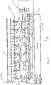
Furthermore, the memory system 38 comprises
operating voltage generating means made available on four
output electric lines a, b, c, d, fitted at one end with
electric contacts K1, K2, K3, K4 respectively. In
particular, said generating means are formed by a
scrambler 41. The scrambler 41 is such as to distribute
the operating voltages to the different output electric
lines a, b, c, d, according to configurations which
depend on the particular operation to be performed on one
or more cells of the array 110 (for example, reading,
programming, erasing) and their position.
A further commutator 42 is provided with an output
connected to one of the two inputs of a sense amplifier
SA. The commutator 42 is such as to connect selectively
its output to one of the electric contacts K1, K2, K3,
K4, depending on the particular cell to be read.
Advantageously, the memory system 38 includes groups
of selection transistors Q1-Q14 which can be
activated/deactivated to/from conduction by means of
command lines L1, L2, L3, L4, to connect the output lines
a, b, c, d, to the main bit lines Main-0 - Main-7
selectively.
In greater detail, each of the first four main bit
lines of the structure 38, i.e. Main-1, Main-2, Main-3
and Main-4, is connected to one of the output lines a, b,
c and d by means of a first group of selection
transistors Q1, Q2, Q3 and Q4. In particular, the
selection transistor Q1 has a first terminal (for example
the drain) connected directly to the main bit line Main-0
and a second terminal (for example the source) connected
directly to the output electric line a.
It will be noted that said first terminal is
intended to be connected to a cell of the matrix, while
the second terminal is intended to receive a suitable
operating voltage.
Furthermore, it should be observed that the words
"connected directly" mean that the respective terminal of
a selection transistor (for example Q1) is connected to
the main bit line (for example Main-0) and to the output
electric line (for example a) by means of respective
electrically conductive paths (for example M1 and M2)
which do not include transistors, but constitute short
circuits. For example, the conductive paths M1, M2 are
formed by means of metallizations.
Similarly, the terminals (for example drain and
source) of the selection transistor Q2 are connected
directly to the main bit line Main-1 and to the output
electric line b.
The selection transistors Q3 and Q4 have a first
terminal connected directly to the main bit lines Main-2
and Main-3 respectively and a second terminal connected
directly to the output electric lines c and d
respectively. The command terminals of the selection
transistors Q1, Q2, Q3, Q4 are connected together in the
node 43 and, therefore, to the same command line L1.
Similarly, the main bit line Main-2 can also be
connected by means of the transistor Q5 to the electric
line a, while the main bit line Main-3 can also be
connected by means of the transistor Q6 to the electric
line b. In particular, the transistor Q5 has a first
terminal connected to the first terminal of the
transistor Q3 and a second terminal connected to the
electric line a, while the transistor Q6 has a first
terminal connected to the first terminal of the
transistor Q4 and a second terminal connected to the
electric line b.
Similarly, each of the other four main bit lines of
the structure 38, i.e. Main-4, Main-5, Main-6 and Main-7,
can be connected to one of the electric lines a, b, c
and d by means of the selection transistors Q9, Q10, Q11
and Q12. In particular, the selection transistors Q9 and
Q10 have a first terminal connected directly to the main
bit lines Main-4 and Main-5 respectively and a second
terminal connected directly to the electric lines a and b
respectively. The selection transistors Q11 and Q12 have
a first terminal connected directly to the main bit lines
Main-6 and Main-7 respectively and a second terminal
connected directly to the electric lines c and d
respectively. The command terminals of the selection
transistors Q9, Q10, Q11, Q12 are connected together in
the node 45 which is connected to the command line L3.
Moreover, the main bit line Main-4 can also be
connected by means of the transistor Q7 to the electric
line c, the main bit line Main-5 can also be connected by
means of the transistor Q8 to the electric line d, the
main bit line Main-6 can also be connected by means of
the transistor Q13 to the electric line a and, finally,
the main bit line Main-7 can also be connected by means
of the transistor Q14 to the electric line b. In
particular, the pairs of transistors Q7,Q9 - Q8,Q10 -
Q11,Q13 - Q12,Q14 have a first terminal in common, while
the second terminal of the transistors Q7,Q8,Q13,Q14 is
connected directly to the electric lines c, d, a, b,
respectively. Finally, the command terminals of the
selection transistors Q5, Q6, Q7, Q8 are connected
together in the node 44 (and therefore to the line L2)
and, similarly, the command terminals of the selection
transistors Q13, Q14 and those of other two selection
transistors (not shown) corresponding to further bit
lines (also not shown) of the array 110 are connected
together in the node 46 (and therefore to the command
line L4).
The structure further comprises a decoder 47
relevant to the entire array of cells and a plurality of
pre-decoding blocks, even if only two are illustrated in
figure 5, i.e. a pre-decoding block P 48 and a pre-decoding
block R 49. Both the decoder 47 and the pre-decoding
blocks 48, 49 are digital blocks formed by
suitable circuit architectures comprising fundamental
logic gates (for example, NAND, NOR, INVERTER).
The decoder 47 is provided in output with a bus 50
including a plurality of command lines L1, L2, L3, L4
connected to the nodes 43, 44, 45, 46, respectively. The
decoder 47 enables selection of the command lines L1-L4
on the basis of address signals coming from the pre-decoding
blocks 48, 49 in order to activate/deactivate
to/from conduction each group of selection transistors
Q1-Q14.
It will be noted that the memory array 110 can be
divided, from the logic-functional point of view, into a
plurality of sub-matrices Sub_Mat_0 - Sub_Mat__3 each of
which can be accessed by a respective group of main bit
lines which, in the embodiment, is composed of four main
bit lines. For example, the sub-matrix Sub__Mat_0 is
accessible by the main bit lines Main-0 - Main-3.
Furthermore, each group of selection transistors is
associated operationally to a particular sub-matrix. For
example, the group Q5,Q6,Q7,Q8 is associated to the sub-matrix
Sub_Mat_1.
A mode of selection of a generic main bit of the
memory array on the basis of the structure 38 in
accordance with the invention will be given below.
The decoder 47 receives, from the pre-decoding
blocks 48, 49, the address of the bit lines to be
selected in the form of a sequence of numeric signals
(sequence of 0 and 1). In fact, the above-mentioned pre-decoding
blocks carry out selection at a higher level as
a result of the large number of main bit lines which are
present in an array of cells. More particularly, the pre-decoding
blocks 48, 49 appropriately decode the external
address signals Ext_Add.
On the basis of the signals received, the decoder 47
activates for conduction the suitable selection
transistors by activating the respective command
terminals by means of signals at two levels: high (logic
1) and low (logic 0). For example, if the nodes
43,44,45,46, visible in figure 5, are polarized by the
signal sequence 1,0,0,0, the transistors Q1,Q2,Q3,Q4
conduct, while all the others are blocked. In this way,
only a first sub-matrix Sub_Mat_0 made up of the first
four main bit lines (Main-0 - Main3) is selected from the
entire array.
If the decoder 47 supplies to the above-mentioned
nodes, for example, the signal sequence 1,1,0,0, the
transistors Q5,Q6,Q7,Q8 conduct as well as the
transistors Q1,Q2,Q3,Q4. In this case, the main bit lines
Main-4 and Main-5 are selected as well as the first four
main bit lines. The additional bit lines Main-4 and Main-5
form, together with the main bit lines Main-2,Main-3, a
second sub-matrix Sub_Mat_1. As can be seen in figure 5,
the sub-matrices Sub_Mat_0 and Sub_Mat_1, which have the
main bit lines Main-2,Main-3 in common, are linked. In
the same way, if the signal sequence is 1,1,1,0 the
transistors Q9,Q10,Q11,Q12 also conduct and the main bit
lines Main-6 and Main-7 are selected. Consequently, the
entire sub-matrix Sub_Mat_2, which is linked to the sub-matrix
Sub_Mat_1, is selected by means of the main bit
lines Main-4,Main-5. Finally, if the decoder 47 supplies
a sequence of only high-level signals (logic 1), the
entire memory array is selected, i.e. all the main bit
lines and all the sub-matrices which are linked to each
other.
Before examining in detail the reading, programming
and erasure operations in the memory array 110 which can
be accessed by means of the selection method described in
figure 5, it is advantageous to recall a phenomenon
linked to the way in which the array is formed.
In fact, as is known, in a contactless type memory
array, the memory cells are contiguous, in other words,
not separated by a suitable insulating region.
It should be noted that in contactless type
structures, the reading signal, i.e. the current present
at the drain terminal of the memory cell to be read, may
be established not only in said cell but also in
contiguous cells. In other words, leakage currents,
possibly of a purely capacitive nature (since they lack
resistive paths) may arise, due to the contiguity of the
memory cells and of the cell bit lines. The leakage
currents are more marked the longer the sequence of
adjacent non-programmed cells.
This undesired phenomenon is known as the neighbor
effect.
Moreover, in the case of dual-bit cells, the need of
reading each cell in two different directions means that
each current path is not univocal, rendering the
formation of undesired paths for the reading current or
sensing current even more likely.
Because of these leakage currents, the reading
current, from which information on the stored data
element is to be derived, may be seriously degraded.
Moreover, these currents do not have constant
characteristics but are dependent on the states
(programmed or non-programmed) of the memory cells
adjacent to the one to be read.
When said degradation arises, it not only weakens
the reading signal but may be a source of misdirections
during the checking steps which may follow a programming
or erasure operation.
This degradation renders the use of current-sensing
techniques for contactless memory arrays more critical
and difficult.
In order to impede said undesired phenomenon, during
reading of a memory array cell in figure 2, an additional
signal, i.e. a biasing voltage V-Bias, is supplied to at
least one cell bit line suitably contiguous to the cell
bit line to which the reading voltage V_Rd is applied.
Said biasing voltage V-Bias produces, between these two
cell bit lines, a potential difference such as to oppose
the establishment of the leakage current between the two
cell bit lines.
More particularly, the closer the biasing voltage V-Bias
is to the reading voltage V_Rd, the greater is the
probability of achieving a condition in which the leakage
current is substantially eliminated.
The table in figure 6 provides an embodiment
illustrating how the main bit lines Main-0,Main-1,Main-2,Main-3
of the sub-matrix Sub_Mat_0 in figure 5 should
be biased during reading, programming and erasure
operations. Similar considerations can be made for the
four main bit lines of each sub-matrix of the array 110.
More particularly, the table is divided into reading
Rd, programming Pg and erasure Er_All sub-tables,
respectively. The sub-tables Rd and Pg refer to reading
and programming operations performed on one generic cell
of the sub-matrix Sub_Mat_0, while the sub-table Er_All
represents the innovative erasure method introduced in
the invention.
For convenience, the following description will
refer both to the cell array 110 in figure 2 where the
main bit lines Main-0, Main-1, Main-2, Main-3 are shown and
to the structure 38 in figure 5.
In this connection, it is assumed that one of the
bits stored in the cell Q44 of the array 110 (for
example, the right-hand bit) is to be read. As seen
previously, the cell under exam must first be activated
by means of the word line WL-4 and, subsequently, the
reading voltage V_Rd and the ground voltage GND must be
applied to the cell bit lines BC-3 and BC-4. As can be
seen from the first line of the reading sub-table Rd, the
reading voltage V_Rd which is applied to the main bit
line Main-1 by means of the electric output line b, is
transferred to the BC-3 through the lower selection
transistor TD-1, while the ground potential GND which is
applied to the main bit line Main-2 is transferred (by
means of the electric output c) to the BC-4 through the
upper selection transistor TU-2.
Moreover, if the cell Q43 (activated by the same
WL-4), adjacent to the Q44, is not programmed, the
phenomenon of leakage current would arise. To avoid this,
the biasing voltage V-Bias which is applied to the main
bit line Main-0 (as indicated in the sub-table Rd) is
transferred by the latter to cell bit line BC-2 through
the upper selection transistor TU-1. Finally, the
scrambler 41 leaves the output line d floating or not
connected and, therefore, the last main bit line Main-3
of the sub-matrix Sub_Mat_0 is also left floating.
These biasing methods are also valid for all the
cells of the column to which the cell Q44 belongs, once
they have been activated by the respective word lines.
In general, in order to read any cell whatsoever of
the array 110, the sub-matrix to which the cell under
exam belongs must first be identified. Subsequently, the
reading voltage V_Rd is applied to a suitable main bit
line of said sub-matrix, while the ground potential GND
and the biasing voltage V-Bias are applied to the main
bit lines adjacent to the one to which the reading
voltage was applied. The fourth main bit line is not
connected.
For example, in order to program one side of the
cell Q43, the procedure given in the first line of the
programming sub-table Pg must be followed. In this case,
after activating the cell Q43 by means of the word line
WL-4, a programming voltage V_Pg which is applied to the
main bit line Main-0 is transferred to the cell bit line
BC-2 through the upper selection transistor TU-1.
Similarly, the ground potential GND which is applied to
the Main-1 is transferred to the cell bit line BC-3
through the lower selection transistor TD-1. The
remaining main bit lines, Main-2 and Main-3, are not
connected.
Said procedure is also valid for all the cells of
the column to which the Q43 belongs, once the respective
word lines have been activated.
In general, having identified the sub-matrix of the
array to which the cell to be programmed belongs, the
programming voltage V_Pg is applied to a suitable main
bit line of said sub-matrix (depending on whether the
right or left-hand bit is to be programmed) and the
ground potential is applied to the main bit line adjacent
to the one to which the reading voltage was applied. The
other main bit lines of the sub-matrix are not connected.
The scrambler 41 of the structure 38 supplies the
reading V_Rd, programming V-Pg and biasing V-Bias
voltages, as well as the ground potential GND, to the
main bit lines of the various sub-matrices linked in the
array 110. More particularly, once the decoder 47 has
selected the sub-matrix of the array where the cell or
group of cells to be read or programmed is located, the
scrambler 41 applies the above voltages to the output
electric lines a,b,c,d, associated to the main bit lines
of the selected sub-matrix. Furthermore, said commutator
42 is connected to one of the electrical contacts
K1,K2,K3,K4 so putting the corresponding output line in
communication with the sense amplifier SA. The sense
amplifier SA compares the intensity of said current with
a reference current, discriminating the bit stored in the
selected side of the cell. For example, in the case of
the reading of cell Q44 already examined, the biasing
voltage V-Bias is applied to the line a, the reading
voltage V_Rd is applied to the line b, the ground
potential GND is applied to the line c, while the line d
is floating (in other words, it is connected to an
ideally infinite impedance). In this case, the commutator
42 is connected to the electrical contact K3 to detect
the intensity of the reading current.
Similarly, in order to program the cell Q43 of the
previous example, the programming voltage V_Pg is applied
to the output line a and the ground potential GND is
applied to the line b. The electric output lines c and d
are not connected or floating.
In the table in figure 6, the sub-table Er_All,
divided into eight lines, describes the erasure method in
a memory array according to the invention.
The first two lines of the sub-table Er_All refer to
the case in which the decoder 47 selects the entire
memory array (All_Sel), i.e. all the main bit lines Main-0
- Main-7 (which are the bit lines visible in figure 2
and figure 5 of the embodiments). For example, in order
to erase the NROM cells of the second and sixth column of
the array 110, the erasure voltage V_Er is first applied
to the Main-0,Main-2 and the Main-1,Main-3 are left
floating. Subsequently, by activating the selection
transistors TU-1,TU-3 and TD-0,TD-2, the voltage V_Er is
applied to the cell bit lines BC-2,BC-6, while the BC-1,BC-5
are left floating. In this way, half of the
information contained in the NROM cells of the second and
sixth column is erased. Subsequently, by applying the
voltage V_Er to the Main-1,Main-3 and leaving Main-0,Main-2
floating (keeping the transistors TU-1,TU-3,TD-0,TD-2
in conduction), erasure of all the cells of the
above-mentioned columns is completed. Afterwards, if
these operations are performed for all the columns in the
array, taking care to apply the erasure voltage V_Er to
the suitable main bit lines and activating the
appropriate selection transistors, the entire memory
array is erased. In fact, the sub-table Er_All
illustrates a method to bias four main bit lines, but
similar considerations are valid for all the main bit
lines of the array.
However, with the decoder 47 it is possible to
select only one portion of the array 110, i.e. a sub-matrix
or a group of sub-matrices (whether linked or
not). In fact, the third and the fourth lines of the sub-table
Er_All refer to the selection of a sub-matrix of
the memory array, for example, the sub-matrix Sub_Mat_0.
By repeating the above-described operations, the
sub-matrix Sub_Mat_0 can be erased entirely or partly, so
obtaining erasure at a lower hierarchical level than
erasure of the entire array and which can be called word
erasure.
The biasing methods described from the fifth to the
eighth line of the sub-table Er_All permit erasure of a
pre-determined portion of the sub-matrix Sub_Mat_0. For
example, if the erasing voltage V_Er is only applied to
the main bit line Main-0 (fifth line), while the others
are left floating, only half of the bits of the cells
connected to said main bit line (through prefixed
selection transistors) are cancelled. The same thing
happens by applying the erasing voltage V_Er to any other
main bit line of the sub-matrix Sub_Mat_0 and leaving the
remaining ones floating. Said selective erasure of the
portion of a sub-matrix is called byte erasure, since it
is at a lower hierarchical level than the previous ones.
As in the cases of reading and programming, in order
to carry out erasure, the scrambler 41 biases the main
bit lines of the sub-matrices with the voltage V_Er or
leaves them floating (not connected) by means of the
electric output lines a,b,c,d and the selection
transistors.
The above considerations are valid for all the sub-matrices
of the memory array 110 which are selected by
the decoder 47, whether independently of each other or
simultaneously.
The present invention has the advantage that the
number of transistors of the selection multiplexer is
lower than those in the prior art and, therefore, both
the total impedance along the path of the current and the
area of silicon occupied by said transistors in the
integrated circuit are also lower.
In this connection, referring to figures 2 and 5, it
will be noted that during a reading and programming
operation of a memory cell, the cell itself is inserted
in a conductive path having a moderate total impedance.
In fact, this conductive path does not include other
transistors besides the cell itself, two upper/lower
selection transistors of the plurality TU-0 - TU-7, TD-0
- TD-7 and two selection transistors of the plurality Q1-Q14.
Furthermore, the reduction in the number of
transistors included in the conductive path is
particularly significant because the selection
transistors are generally bigger than the memory cells
NROM.
Moreover, the erasure operation is performed with
the same circuits (scrambler, electric lines, selection
transistors) as those which are used for the reading and
programming operations; therefore, use of the erasure
regulator and relative transistors is avoided with
considerable saving of room on the chip.
The erasure operation according to the invention
also makes it possible to erase portions of the memory
array selectively, i.e. sub-matrices or portions of sub-matrices,
as well as the entire array, unlike the
techniques of the prior art.
It should be observed that according to a particular
embodiment of the memory system 38, this can also include
other memory arrays (similar to the array 110) relative
to other bits of a memory word, the least significant bit
of which is stored by the array 110. Therefore, during a
reading operation, the decoder 47, by means of suitable
lines forming part of the bus 50, can simultaneously
select other main bit lines forming part of said other
memory arrays. In this way, reading in parallel of
several bits associated to all the memory arrays is
possible. The operations of programming and erasing can
be performed in the same way.
Naturally, in order to satisfy contingent and
specific requirements, a person skilled in the art may
apply to the above-described selection method many
modifications and variations, all of which, however, are
included within the scope of protection of the invention
as defined by the appended claims.