EP1434067A1 - Optical filter module, and manufacturing method thereof - Google Patents
Optical filter module, and manufacturing method thereof Download PDFInfo
- Publication number
- EP1434067A1 EP1434067A1 EP02800767A EP02800767A EP1434067A1 EP 1434067 A1 EP1434067 A1 EP 1434067A1 EP 02800767 A EP02800767 A EP 02800767A EP 02800767 A EP02800767 A EP 02800767A EP 1434067 A1 EP1434067 A1 EP 1434067A1
- Authority
- EP
- European Patent Office
- Prior art keywords
- optical
- filter
- groove
- insertion groove
- plane substrate
- Prior art date
- Legal status (The legal status is an assumption and is not a legal conclusion. Google has not performed a legal analysis and makes no representation as to the accuracy of the status listed.)
- Withdrawn
Links
Images






Classifications
-
- G—PHYSICS
- G02—OPTICS
- G02B—OPTICAL ELEMENTS, SYSTEMS OR APPARATUS
- G02B6/00—Light guides; Structural details of arrangements comprising light guides and other optical elements, e.g. couplings
- G02B6/10—Light guides; Structural details of arrangements comprising light guides and other optical elements, e.g. couplings of the optical waveguide type
- G02B6/12—Light guides; Structural details of arrangements comprising light guides and other optical elements, e.g. couplings of the optical waveguide type of the integrated circuit kind
- G02B6/12007—Light guides; Structural details of arrangements comprising light guides and other optical elements, e.g. couplings of the optical waveguide type of the integrated circuit kind forming wavelength selective elements, e.g. multiplexer, demultiplexer
-
- G—PHYSICS
- G02—OPTICS
- G02B—OPTICAL ELEMENTS, SYSTEMS OR APPARATUS
- G02B6/00—Light guides; Structural details of arrangements comprising light guides and other optical elements, e.g. couplings
- G02B6/24—Coupling light guides
- G02B6/26—Optical coupling means
- G02B6/28—Optical coupling means having data bus means, i.e. plural waveguides interconnected and providing an inherently bidirectional system by mixing and splitting signals
- G02B6/293—Optical coupling means having data bus means, i.e. plural waveguides interconnected and providing an inherently bidirectional system by mixing and splitting signals with wavelength selective means
- G02B6/29346—Optical coupling means having data bus means, i.e. plural waveguides interconnected and providing an inherently bidirectional system by mixing and splitting signals with wavelength selective means operating by wave or beam interference
- G02B6/29361—Interference filters, e.g. multilayer coatings, thin film filters, dichroic splitters or mirrors based on multilayers, WDM filters
- G02B6/29368—Light guide comprising the filter, e.g. filter deposited on a fibre end
-
- G—PHYSICS
- G02—OPTICS
- G02B—OPTICAL ELEMENTS, SYSTEMS OR APPARATUS
- G02B6/00—Light guides; Structural details of arrangements comprising light guides and other optical elements, e.g. couplings
- G02B6/24—Coupling light guides
- G02B6/26—Optical coupling means
- G02B6/28—Optical coupling means having data bus means, i.e. plural waveguides interconnected and providing an inherently bidirectional system by mixing and splitting signals
- G02B6/293—Optical coupling means having data bus means, i.e. plural waveguides interconnected and providing an inherently bidirectional system by mixing and splitting signals with wavelength selective means
- G02B6/29379—Optical coupling means having data bus means, i.e. plural waveguides interconnected and providing an inherently bidirectional system by mixing and splitting signals with wavelength selective means characterised by the function or use of the complete device
- G02B6/2938—Optical coupling means having data bus means, i.e. plural waveguides interconnected and providing an inherently bidirectional system by mixing and splitting signals with wavelength selective means characterised by the function or use of the complete device for multiplexing or demultiplexing, i.e. combining or separating wavelengths, e.g. 1xN, NxM
Definitions
- the present invention relates to an optical filter module for optical communication that incorporates various kinds of optical filters therein and to a method of manufacturing the optical filter module.
- optical fiber amplifier Used as a system for amplifying this attenuated light is an optical fiber amplifier. Being capable of amplifying the output without converting optical signals into electrical signals, the optical fiber amplifier is a system essential to an optical communication network.
- Fig. 8A shows an example of the structure of the system.
- An optical fiber amplifier is made of optical isolator 53, erbium-doped optical fiber 51, pumping laser 54 used as laser light for excitation, photodiode 52 for monitoring output, and filter 55 for adjusting gains.
- pumping laser 54 for a single-mode fiber laser light having a wavelength of 1.48 ⁇ m is used.
- amplification gains of erbium-doped optical fiber 51 are dependent on frequencies, as shown by characteristics A of Fig. 8B. Therefore, it is necessary to insert filter 55 having characteristics B, i.e. the inverse of characteristics A, into the transmission path after the amplification of optical output and flatten the amplification gains as shown by characteristics C.
- Filter 55 is called a gain-flattening filter.
- filter 55 is used as a part of a module that incorporates the filter inserted between optical fibers.
- Fig. 8C shows the structure of the module. In the module, optical fibers 56, collimating and collective lenses 57, and gain-flattening filter 58 are housed and sealed into metal housing 59 after optical axis adjustment.
- the lenses themselves have certain sizes, and distances between the optical passages and the lenses necessary for focusing are required. Therefore, the size reduction of the entire module is restricted to a certain degree.
- each of the optical passages must be connected accurately.
- adjustment of the lenses requires cost and time: thus, productivity of the module is poor.
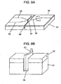
- Figs. 9A and 9B are drawings showing the structure of the invention.
- the invention is an example of a reflection type optical multiplexer/demultiplexer for wavelength division multiplexing (WDM) in which a filter insertion groove is formed so as to intersect embedded optical waveguides formed on a silicon substrate, and a multilayered filter is inserted and integrated in the groove.
- WDM wavelength division multiplexing
- Passages for guiding the waves of light are formed in one surface of clad material 32 on silicon substrate 31 as waveguides.
- Filter insertion groove 36 is formed so as to intersect the waveguides. This structure eliminates the need of adjustment of optical axes of input waveguide 33 and output waveguides 35 and 34.
- width Dg of filter insertion groove 36 and radius of curvature R of the warp of multilayered filer 37(hereinafter referred to as a "filter”) are set so as to satisfy the following relation: R ⁇ W 2 /8(Dg-Df) where the lateral width of filter 37 is W, and the thickness thereof is Df, .
- This relation proposes a structure in which filter 37 can securely be fitted in filter insertion groove 36 utilizing the warp of filter 37.
- proposed is a module structure in which embedded optical waveguides form optical waveguide paths, and various kinds of filters are inserted and integrated in the paths.
- filter 37 has a warp having at least a certain radius of curvature. Therefore, when the filter isn't mounted at the exactly correct position, the angle of incidence to filter 37 is largely displaced. Further, when embedded waveguides are used as optical waveguide paths, the warp of multilayered filter 37 inevitably generates a gap between the multilayered filter and waveguides 35 and 33 in filter insertion groove 36. This gap causes scattering and loss of light from waveguides 35 and 33. Additionally, it is extremely difficult and thus disadvantageous for production to mechanically hold and insert a warped component in a microgroove.
- Proposed is an optical filter module in which a filter insertion groove is formed so as to intersect optical passages on a plane substrate, a filter is inserted in this filter insertion groove, and covers cover the optical passages so as to be bonded onto the plane substrate.
- Fig. 1A shows a top view of an optical filter module having two optical passes in accordance with a first exemplary embodiment of the present invention.
- Fig. 1B shows a side view thereof.
- Fig. 1C shows a sectional view thereof.
- Filter 2 is inserted in a filter insertion groove 1 (hereinafter referred to as a "groove"), and bonded by optical adhesive 6.
- Each of optical fibers 4 for forming optical passages is provided in a space that is formed by V-shaped groove 10, formed on the principle surface of plane substrate 5, and covers 3.
- optical passages are not necessarily integrated with plane substrate 5. This renders greater general versatility to materials of the optical passages and plane substrate.
- an optical passage that is not integrated with plane substrate 5, such as optical fiber 4 is used, precise V-shaped groove 10 is formed on plane substrate 5 for fixation of optical fiber 4.
- the V-shaped groove is used as a guide for fixation of optical fiber 4.
- Production of filter insertion groove 1 so as to intersect V-shaped grooves 10 facilitates insertion and connection of filter 2, without causing misalignment of the optical axes of optical fibers 4. Further, the extremely simple structure allows downsizing of the module and improvement of productivity thereof.
- Filter 2 is formed by laminating a large number of dielectric thin films made of a material, e.g. SiO 2 and Ta 2 O 5 , on a resin substrate made of a material, e.g. glass and polyimide.
- a material e.g. SiO 2 and Ta 2 O 5
- Covers 3 and plane substrate 5 are formed of glass, silicon, or other materials. Desirably, the covers and plane substrate have linear expansion coefficients approximating to that of optical fibers 4. However, when a resin-based adhesive (not shown) is used for bonding them, the elasticity of the adhesive can alleviate the stress caused by the difference in liner expansion coefficient. When a photo-curing adhesive is used, it is desirable that the covers and plane substrate are made of optically transparent materials.
- optical adhesive 6 having a refractive index substantially equal to that of a material used for optical fibers 4 is used as optical adhesive 6.
- optical adhesive 6 having a refractive index approximating to 1.44, i.e. the refractive index of fused silica.
- V-shaped grooves 10 formed on covers 3 and plane substrate 5 need not have the same depth and angle necessarily.
- the angle and depth of V-shaped groove 10 formed on cover 3 are set to values equal to or larger than those of a portion of optical fiber 4 projecting from the principle surface of plane substrate 5, when optical fiber 4 is mounted in V-shaped groove 10 on plane substrate 5.
- cover 3 and plane substrate 5 allow the optical fiber to be mounted and clamped securely.
- Groove 1 in plane substrate 5 is formed to have a predetermined angle of ⁇ with respect to optical fibers 4. This is for preventing light incident from optical fibers 4 upon filter 2 from reflecting.
- the tilt angle depends on the wavelength of light to be guided. For example, when light having a wavelength of 1.48 ⁇ m is guided using a single-mode fiber, it is desirable to provide a tilt angle ⁇ ranging from approx. 5 to 10 degrees. For a tilt angle ⁇ smaller than 5 degrees, reflection has greater influence. For a tilt angle ⁇ exceeding 10 degrees, refraction makes it difficult to set the optical axes, and affects the characteristics of filter 2.
- a groove is formed across continuous lengths of optical passages and a filter is inserted therein.
- the optical filter module of this embodiment is structured so that groove 1 is formed so as to intersect optical passages 4 and filter 2 is inserted therein. Because of this structure, optical fibers 4 are cut by groove 1, and gap G having a width of groove 1 exists between the endfaces of optical fibers 4 via filter 2.
- TEC thermally expanded core
- This optical fiber is a special one in which a doped element for controlling the refractive index of the core, such as GeO 2 , is diffused to a part of the clad by heating a part of the clad, to substantially expand the core diameter.
- the use of this kind of optical fiber increases the spot size of light emitted from each endface of optical fibers 4.
- groove 1 is machined and formed so as to intersect the largest portion of the core diameter expanding part in each optical passage 4.
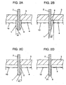
- Figs. 2A through 2D are applicable as the shape of groove 1.
- the bottom of groove 1 shown in Fig. 2A is shaped to be shallower on the sides of both groove walls, and have a flat portion at the center of the bottom of which central portion is deeper at an angle of ⁇ 1.
- Fig. 2B shows a case where groove 1 has a certain angle of ⁇ 2 from the bottom to the principle surface of plane substrate 5 on the side of one of groove walls.
- Fig. 2C shows a case where a part of the bottom of groove 1 has a flat portion on the side of one of groove walls, and the bottom has a certain angle of ⁇ 3 from the flat portion to the side of the other groove wall.
- the bottom of groove 1 is shaped semi-circular.
- Each of these grooves 1 is formed using a diamond grindstone having a tip previously formed into the shape of the groove, for example. Because groove 1 is formed by transferring the shape of the tip of the diamond grindstone to the groove shape, the groove shape after machining largely depends on the forming accuracy of the diamond grindstone. When the width of a grindstone is up to 0.1 mm, machining is difficult because the diameters of usable diamond particles are restricted. However, when the width of the grindstone exceeds 0.1 mm, machining the shapes is relatively easy.
- groove 1 is machined to irregular shapes so that the tilt angle formed by one groove wall with the other is small.
- the reason for machining in this manner is to prevent filter 2 from tilting after insertion.
- groove 1 is formed using the endface of cover 3 previously mounted as a reference surface, force is exerted in the direction in which the diamond grindstone for machining is forced toward cover 3, i.e. the reference surface, during machining. In order to prevent deterioration of machining accuracy of groove 1 caused by meander of the diamond grindstone, such machining is effective.
- Groove 1 shown in Fig. 2B has the effects equivalent to those of groove 1 shown in Fig. 2A. Additionally, forming the section of groove 1 into a V shape as shown in Fig. 2B allows filter 2 that is even extremely thin for groove 1 to be fixed securely as long as it is inserted as far as it goes. In other words, the V-shaped groove broadens the allowable range of the thickness of filter 2 with respect to groove 1.
- Groove 1 shown in Fig. 2C has the effects equivalent to those of groove 1 shown in Fig. 2A. Additionally, forming the bottom surface of groove 1 semi-circular as shown in Fig. 2C facilitates machining in production of groove 1. Further, because the bottom surface is curved, the angle at which filter 2 is erected in groove 1 can freely be set in the range of the width of the groove.
- Groove 1 shown in Fig. 2D has the effects equivalent to those of groove 1 shown in Fig. 2A. Additionally, groove 1 as shown in Fig. 2D has a bottom tapered from one of groove walls to the other. Because one groove wall is not tapered, filter 2 can be fixed along the surface. Further, even when optical fibers 4 and covers 3 are attached before machining of the groove, groove lof such a shape can be formed without a bit hitting covers 3 or displaced from the endfaces of the covers during machining.
- the optical filter module has two optical fibers.
- an optical filter module having one optical passage can be fabricated.
- Fig. 3A shows a top view of an optical filter module in accordance with a second exemplary embodiment.
- Fig. 3B shows a side view thereof.
- Fig. 3C shows a sectional view thereof.
- a minute angle ⁇ is provided in order to prevent scattering and reflection caused by filter insertion groove 1.
- this minute angle ⁇ is not provided.
- a minute angle ⁇ is provided in groove 1 in the side view of Fig. 3B.
- this embodiment has a structure and effects similar to those of the first exemplary embodiment.
- a more multi-functional optical filter module having two or more optical passages can also be fabricated.
- Figs. 4A through 4G are sectional views sequentially showing a procedure of fabricating an optical filter module of the present invention.
- a necessary number of V-shaped grooves 10 for fixing optical fibers 4 forming optical passages are precisely formed on plane substrate 5 shown in Fig. 4A.
- filter insertion groove 1 sufficiently wide for the thickness of filter 2 is formed so as to intersect these precise V-shaped grooves 10.
- groove 1 is formed so as to be displaced at a minute angle of ⁇ from the right angle of the optical passages. Specifically, ⁇ ranges from 5 to 10 degrees, and is changed according to the wavelength of light to be used. Placing filter 2 along the wall surface of groove 1 formed at an arbitrary angle required allows filter 2 to be fixed at the arbitrary angle designed.
- Groove 1 is formed to have an appropriate shape selected from the structures shown in Figs. 2A through 2D.
- groove 1 is formed by grinding with a grindstone shaped to the groove using cubic boron nitride or diamond as abrasive grains, or machining using particles, such as blasting.
- silicon is used as a material of plane substrate 5, wet etching or dry etching can also be used.
- a formed grindstone allows production of the irregular shapes more freely and thus is more advantageous.
- each optical fiber 4 is installed in corresponding V-shaped groove 10.
- the portion of mounted optical fiber 4 is a clad portion with coating removed, in consideration with mounting accuracy.
- the angle and depth of each V-shaped groove 10 are set so that each optical fiber 4 is flush with the principle surface of plane substrate 5.
- the use of core diameter expanding fibers as optical fibers 4 can increase the spot size of each of the endfaces of optical fibers 4 and decrease the transmission loss and connection loss between optical fibers 4.
- optical fibers 4 are installed so that the core diameter thereof is largest in groove 1.
- optical adhesive 6 is applied to the entire principle surface of plane substrate 5. Further, as shown Fig. 4E, filter 2 is inserted in groove 1 having optical adhesive 6 charged therein. At this time, the size of filter 2 is set so that the upper portion of filter 2 always projects from the principle surface of plane substrate 5. Additionally, the inside of groove 1 formed in the second step is also filled with optical adhesive 6.
- optical adhesive 6 having a refractive index substantially equal to that of the core material of optical fibers 4 to be used can decrease the connection loss between the optical fibers.
- Methods of curing optical adhesive 6 include using light, e.g. ultraviolet light, and heating. The method of using light is advantageous for reducing production time.
- covers 3 are moved from both sides of filter 2 projecting from groove 1 to sandwich and clamp the filter on both sides.
- mounting one of covers 3 so that the side face thereof is aligned with one of the side faces of groove 1 allows filter 2 to be mounted and fixed along the side face of groove 1.
- This method eliminates the need of registering two sheets of covers 3 at the same time and thus simplifies fabrication of the optical filter module. Additionally, when filter 2 is clamped at an angle, fixing one of the covers makes it easy to adjust the angle. This method is also useful to prevent breakage of filter 2 when the filter is sandwiched by the other cover 3.
- the sandwiched portion is a projecting portion of filter 2.
- the length of the projecting portion of filter 2 is at least half the thickness of cover 3 in consideration of the strength of filter 2, because filter 2 is sandwiched by covers 3.
- the projecting portion is made longer to increase the area sandwiched by covers 3: thus, the warp is straitened.
- glass or other material is used for the substrate of filter 2, its large elastic modulus is effective in preventing breakage caused by stress.
- the optical filter module is completed by irradiating covers 3 and/or plane substrate 5 with light, such as ultraviolet light, or heating, to cure the adhesive.
- light such as ultraviolet light, or heating
- the use of a photo-curing adhesive or heat-hardening adhesive as adhesive 6 allows covers 3 to be bonded without application of mechanical pressure.
- the optical axes of optical fibers 4 are unlikely to be misaligned. Additionally, the time taken for mounting can be reduced.
- Figs. 5A through 5G show a procedure of fixing optical fibers 4 on plane substrate 5, and then forming filter insertion groove 1 in plane substrate 5 and inserting filter 2 therein.
- a necessary number of V-shaped grooves for fixing optical fibers 4 are precisely formed on the principle surface of plane substrate 5.
- the angle and depth of each V-shaped groove 10 are set so that each optical fiber 4 is flush with the principle surface of plane substrate 5.
- each optical fiber 4 is installed in corresponding V-shaped groove 10.
- the use of core diameter expanding fibers as optical fibers 4 is effective in increasing the spot size of each of the endfaces of optical fibers 4 and decreasing the transmission loss and connection loss between optical fibers 4.
- each optical fiber 4 is installed so that the core diameter thereof is largest in a place where groove 1 is to be formed.
- groove 1 sufficiently wide for the thickness of filter 2 is formed so as to be displaced at a minute angle of ⁇ from the right angle of optical fibers 4.
- optical fibers 4 are cut at the same time.
- abrasive grains it is desirable to use abrasive grains as small as possible in machining.
- a diamond grindstone is used to form groove 1.
- the endfaces of optical fibers 4 like a mirror surface can be obtained by selecting diamond abrasive grains of at least #3000 (average particle diameter: up to 5 ⁇ m).
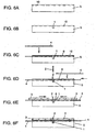
- Figs. 6A through 6F show a procedure of fixing optical fibers 4 at one of the endfaces of a groove, inserting filter 2 therein, and then placing the other optical fibers 4 against the filter.
- a necessary number of V-shaped grooves 10 for fixing optical fibers 4 are precisely formed on the principle surface of plane substrate 5.
- the angle and depth of each V-shaped groove 10 are set so that each optical fiber 4 is flush with the principle surface of plane substrate 5.
- filter insertion groove 1 sufficiently wide for the thickness of filter 2 is formed so as to intersect V-shaped grooves 10.
- groove 1 is formed so as to be displaced at a minute angle of ⁇ from the right angle of the optical passages.
- an appropriate shape is selected from the structures shown in Figs. 2A through 2D.
- optical adhesive 6 is applied to the entire principle surface of plane substrate 5. Either optical fibers 4 for input or optical fibers 4 for output is placed in corresponding V-shaped grooves 10.
- filter 2 is inserted in groove 1.
- the other optical fibers 4 are inserted as they are slid along corresponding V-shaped grooves 10.
- the other optical fibers are placed against filter 2 so that the gap between filter 2 and the other optical fibers 4 is as small as possible.
- This placement can considerably decrease attenuation of light caused by scattering, irregular reflection and changes in refractive index.
- the use of core diameter expanding fibers as optical fibers 4 is effective in increasing the spot size of each of the endfaces of optical fibers 4 and decreasing the transmission loss and connection loss between optical fibers 4.
- Each optical fiber 4 is installed so that the core diameter thereof is largest in groove 1.
- Figs. 7A through 7F show a procedure followed when optical passages 20 have already been embedded in plane substrate 5.
- FIG. 7A When optical passages 20, such as diffusion glass waveguides and polymer waveguides, are embedded in plane substrate 5, as shown Fig. 7A, V-shaped grooves 10 need not be formed.
- FIG. 7B groove 1 sufficiently wide for the thickness of filter 2 is formed so as to be displaced at a minute angle of ⁇ from the right angle of the optical passages.
- adhesive 6 is applied to the top surface of plane substrate 5 as shown in Fig. 7C, and filter 2 is inserted therein as shown in Fig. 7D. At this time, adhesive 6 having a refractive index as equal as possible to that of optical passages 20 is selected.
- two sheets of covers 3 placed on plane substrate 5 are moved as shown in Fig. 7E, to sandwich filter 2. At this time, filter 2 is clamped at a predetermined angle.
- Fig. 7F filter 2 is sandwiched at a desired angle and bonded using light or heat.
- Fixing optical passages using precise V-shaped grooves so as to avoid misalignment of optical axes thereof facilitates optical axis adjustment, which is supposed to be most critical and difficult in connection of optical passages.
- Forming a filter insertion groove so as to be displaced at a minute angle of ⁇ from the right angle of the optical axes can prevent entry of reflected or scattered light caused by the wall surfaces of the groove.
- Selecting a filter insertion groove having a shape most appropriate for a filter to be inserted allows more precise connection between the filter and the optical passages.
- it is difficult to insert a filter while precisely aligning optical axes. There are also problems in downsizing. This structure can provide an extremely small optical filter module easily.
Landscapes
- Physics & Mathematics (AREA)
- General Physics & Mathematics (AREA)
- Optics & Photonics (AREA)
- Engineering & Computer Science (AREA)
- Microelectronics & Electronic Packaging (AREA)
- Optical Couplings Of Light Guides (AREA)
- Light Guides In General And Applications Therefor (AREA)
Abstract
Description
Claims (20)
- An optical filter module comprising:an optical passage;a plane substrate having said optical passage and a filter insertion groove formed so as to intersect said optical passage;a filter inserted in said filter insertion groove; anda cover covering said optical module and bonded to said plane substrate.
- The optical filter module of claim 1, wherein
said optical passage has an intersection; and
said filter insertion groove intersects said intersection. - The optical filter module of claim 1, wherein said optical passage is an optical fiber.
- The optical filter module of claim 1, wherein said optical passage is a core diameter expanding fiber.
- The optical filter module of claim 4, wherein an endface of said optical passage faced to a wall surface of said filter insertion groove is a portion having an expanded core diameter of said core diameter expanding fiber.
- The optical filter module of claim 1, wherein a bottom of said filter insertion groove is formed to have a shape tapered from both groove wall surfaces toward a bottom surface thereof.
- The optical filter module of claim 1, wherein a bottom of said filter insertion groove is formed to have a V-shaped section.
- The optical filter module of claim 1, wherein a bottom of said filter insertion groove is formed to have a semi-circular section.
- The optical filter module of claim 1, wherein a bottom of said filter insertion groove is formed to have a shape tapered from one of groove wall surfaces toward the other.
- The optical filter module of claim 1, wherein said filter is fixed along one of groove wall surfaces of said filter insertion groove.
- The optical filter module of claim 1, comprising a plurality of said covers, wherein a portion of said filter projecting from said filter insertion groove is sandwiched between said plurality of covers.
- The optical filter module of claim 11, wherein a length of the portion of said filter projecting from said filter insertion groove is at least half the thickness of each of said covers.
- The optical filter module of claim 1, wherein an angle formed by said optical passage with said filter ranges from 5 to 10 degrees.
- The optical filter module of claim 13, wherein the angle formed by said optical passage with said filter is provided on a principle surface of said plane substrate.
- The optical filter module of claim 13, wherein the angle formed by said optical passage with said filter is provided in a direction perpendicular to the principle surface of said plane substrate.
- The optical filter module of claim 1, wherein at least one of said plane substrate and said cover is fabricated to form a V-shaped groove thereon for receiving said optical passage.
- The optical filter module of claim 1, wherein said cover and said plane substrate are bonded together using one of a photo-curing adhesive and a heat-hardening adhesive.
- A method of manufacturing an optical filter module comprising the steps of:forming a filter insertion groove so that said groove intersects an optical passage formed in a plane substrate;inserting a filter in said filter insertion groove;moving a cover placed on said plane substrate to support a portion of said filter projecting from said filter insertion groove with said cover; andbonding said cover onto said plane substrate.
- The method of manufacturing an optical filter module of claim 18 further comprising the steps of:forming a V-shaped groove on said plane substrate; andforming said optical passage in said V-shaped groove.
- A method of manufacturing an optical filter module comprising the steps of:forming a V-shaped groove on a plane substrate;forming a filter insertion groove so that said groove intersects said V-shaped groove;forming optical passages so that one end of each of said optical passages corresponds to said filter insertion groove;inserting a filter in said filter insertion groove;moving a cover placed on said plane substrate to support a portion of said filter projecting from said filter insertion groove with said cover; andbonding said cover onto said plane substrate.
Applications Claiming Priority (3)
| Application Number | Priority Date | Filing Date | Title |
|---|---|---|---|
| JP2001308309 | 2001-10-04 | ||
| JP2001308309A JP2003114334A (en) | 2001-10-04 | 2001-10-04 | Optical filter module and method of manufacturing the same |
| PCT/JP2002/010360 WO2003032032A1 (en) | 2001-10-04 | 2002-10-04 | Optical filter module, and manufacturing method thereof |
Publications (2)
| Publication Number | Publication Date |
|---|---|
| EP1434067A1 true EP1434067A1 (en) | 2004-06-30 |
| EP1434067A4 EP1434067A4 (en) | 2005-05-25 |
Family
ID=19127642
Family Applications (1)
| Application Number | Title | Priority Date | Filing Date |
|---|---|---|---|
| EP02800767A Withdrawn EP1434067A4 (en) | 2001-10-04 | 2002-10-04 | OPTICAL FILTER MODULE AND METHOD OF MANUFACTURE |
Country Status (6)
| Country | Link |
|---|---|
| US (1) | US7044649B2 (en) |
| EP (1) | EP1434067A4 (en) |
| JP (1) | JP2003114334A (en) |
| CN (1) | CN1206548C (en) |
| TW (1) | TWI229754B (en) |
| WO (1) | WO2003032032A1 (en) |
Families Citing this family (4)
| Publication number | Priority date | Publication date | Assignee | Title |
|---|---|---|---|---|
| JP4056941B2 (en) * | 2003-06-17 | 2008-03-05 | Smk株式会社 | Optical fixed attenuator and manufacturing method thereof |
| CN103630977B (en) * | 2013-12-18 | 2016-01-27 | 湖南理工学院 | A kind of waveguide mode control method of based thin film type spatial filter |
| EP4049074A4 (en) | 2019-10-25 | 2023-11-15 | CommScope Technologies LLC | Integrated optical wavelength division multiplexing devices |
| TWI809270B (en) * | 2020-04-29 | 2023-07-21 | 日商東洋克斯股份有限公司 | Sleeves for pipe joints |
Family Cites Families (27)
| Publication number | Priority date | Publication date | Assignee | Title |
|---|---|---|---|---|
| JPS6434604A (en) | 1987-07-24 | 1989-02-06 | Kobe Steel Ltd | Tool exchanger for shearing machine |
| JPS6434604U (en) * | 1987-08-25 | 1989-03-02 | ||
| JPH0284601A (en) | 1988-06-29 | 1990-03-26 | Furukawa Electric Co Ltd:The | Optical parts and its production |
| JPH0234806A (en) * | 1988-07-25 | 1990-02-05 | Sumitomo Electric Ind Ltd | Demultiplexer and multiplexer and its manufacturing method |
| JP2893268B2 (en) * | 1989-04-08 | 1999-05-17 | 株式会社フジクラ | Zirconia connector ferrule with optical fiber filter connector |
| JPH02284103A (en) * | 1989-04-26 | 1990-11-21 | Furukawa Electric Co Ltd:The | Optical parts and production thereof |
| JPH0634837A (en) * | 1992-07-15 | 1994-02-10 | Sumitomo Electric Ind Ltd | Optical component |
| JPH0659143A (en) * | 1992-08-07 | 1994-03-04 | Furukawa Electric Co Ltd:The | Waveguide with filter |
| JPH075346A (en) * | 1993-06-18 | 1995-01-10 | Sumitomo Osaka Cement Co Ltd | Optical fiber fixing means for optical element and method for connecting and fixing optical fiber to optical element |
| JPH07281049A (en) * | 1994-04-11 | 1995-10-27 | Fuji Elelctrochem Co Ltd | Method for manufacturing fiber integrated optical component |
| JP3247021B2 (en) | 1994-12-26 | 2002-01-15 | 古河電気工業株式会社 | Optical fiber type optical filter |
| JPH08184712A (en) * | 1995-01-06 | 1996-07-16 | Furukawa Electric Co Ltd:The | Optical fiber type optical filter |
| JPH08211228A (en) * | 1995-02-06 | 1996-08-20 | Furukawa Electric Co Ltd:The | Filtered optical fiber |
| JP3500765B2 (en) * | 1995-04-25 | 2004-02-23 | 住友電気工業株式会社 | Optical filter manufacturing method |
| JPH0921912A (en) | 1995-07-05 | 1997-01-21 | Furukawa Electric Co Ltd:The | Dielectric multilayer filter, manufacturing method thereof, and structure for inserting dielectric multilayer filter into optical waveguide |
| JPH0961664A (en) | 1995-08-21 | 1997-03-07 | Fujitsu Ltd | Optical transmission equipment parts |
| JP3175814B2 (en) | 1995-10-09 | 2001-06-11 | 日本電信電話株式会社 | Waveguide optical device and method of manufacturing the same |
| JPH1048439A (en) | 1996-08-02 | 1998-02-20 | Japan Aviation Electron Ind Ltd | Optical filter |
| JPH10300936A (en) | 1997-04-24 | 1998-11-13 | Matsushita Electric Ind Co Ltd | Optical communication component with built-in optical filter and method of manufacturing the same |
| JPH10307221A (en) | 1997-05-09 | 1998-11-17 | Hitachi Ltd | Semiconductor optical coupling device and assembling method thereof |
| JP3708306B2 (en) | 1997-10-06 | 2005-10-19 | 富士通株式会社 | Wavelength division multiplexing optical device and manufacturing method thereof |
| US6215655B1 (en) * | 1997-10-31 | 2001-04-10 | Lacerta Enterprises, Inc. | Drive-in ordering apparatus |
| JP3804888B2 (en) | 1997-12-03 | 2006-08-02 | 松下電器産業株式会社 | Optical waveguide parts |
| JP3716118B2 (en) | 1998-12-25 | 2005-11-16 | 京セラ株式会社 | Optical module |
| US6535655B1 (en) * | 2000-01-18 | 2003-03-18 | Corning Incorporated | Fiberoptic polarizer and method of making the same |
| JP2002189151A (en) * | 2000-10-11 | 2002-07-05 | Matsushita Electric Ind Co Ltd | Optical receiving module, optical transmitting and receiving module and manufacturing method |
| JP2003114335A (en) * | 2001-10-04 | 2003-04-18 | Matsushita Electric Ind Co Ltd | Optical filter module and method of manufacturing the same |
-
2001
- 2001-10-04 JP JP2001308309A patent/JP2003114334A/en active Pending
-
2002
- 2002-10-03 TW TW091122876A patent/TWI229754B/en not_active IP Right Cessation
- 2002-10-04 CN CNB028042115A patent/CN1206548C/en not_active Expired - Fee Related
- 2002-10-04 US US10/470,295 patent/US7044649B2/en not_active Expired - Fee Related
- 2002-10-04 WO PCT/JP2002/010360 patent/WO2003032032A1/en not_active Ceased
- 2002-10-04 EP EP02800767A patent/EP1434067A4/en not_active Withdrawn
Also Published As
| Publication number | Publication date |
|---|---|
| JP2003114334A (en) | 2003-04-18 |
| WO2003032032A1 (en) | 2003-04-17 |
| US7044649B2 (en) | 2006-05-16 |
| US20040114876A1 (en) | 2004-06-17 |
| CN1489709A (en) | 2004-04-14 |
| CN1206548C (en) | 2005-06-15 |
| TWI229754B (en) | 2005-03-21 |
| EP1434067A4 (en) | 2005-05-25 |
Similar Documents
| Publication | Publication Date | Title |
|---|---|---|
| KR101258725B1 (en) | Wideband optical coupling into thin soi cmos photonic integrated circuit | |
| US7187826B2 (en) | Multiple-port optical package and DWDM module | |
| US6582135B2 (en) | Method of matching optical elements and fiber ferrules | |
| US20020196998A1 (en) | Optical assembly for coupling with integrated optical devices and method for making | |
| US7123798B2 (en) | Optical device and method of producing the same | |
| US10094989B2 (en) | Optical device, optical processing device, and method of producing the optical device | |
| US7172344B2 (en) | Optical filter module and manufacturing method thereof | |
| JP2003294992A (en) | Optical device | |
| US7044649B2 (en) | Optical filter module, and manufacturing method thereof | |
| EP1496377A2 (en) | Optical multiplexer/demultiplexer, optical integrated circuit and light transceiver using the same | |
| US20210026080A1 (en) | Optical receptacle and optical transceiver | |
| JP3914450B2 (en) | Optical device and manufacturing method thereof | |
| EP1816501B1 (en) | Optical demultiplexing device | |
| US7394955B2 (en) | Optical component and method of manufacturing the same | |
| US7039279B2 (en) | Optical filter module and manufacturing method thereof | |
| JP2002277688A (en) | Fiber array substrate, fixing structure of optical fiber array using the substrate, substrate for positioning optical fiber, and fixing structure of optical fiber using the positioning substrate | |
| KR20050071967A (en) | Optical transmitter of bidirectional optical module and method for fabricating the same | |
| JP5148506B2 (en) | Optical device and optical transceiver using the same | |
| WO2024215681A1 (en) | Plc waveguide devices incorporating thin filters and method of making same | |
| JP4140094B2 (en) | Optical waveguide device and manufacturing method thereof | |
| JP2004302454A (en) | Optical monitor module | |
| WO2021106163A1 (en) | Optical fiber array | |
| JP2005265947A (en) | Optical composite device, optical transmitting-receiving module, and manufacturing method of optical composite device | |
| JP2005134572A (en) | Optical waveguide circuit | |
| WO2004011982A1 (en) | Optical device and production method therefor |
Legal Events
| Date | Code | Title | Description |
|---|---|---|---|
| PUAI | Public reference made under article 153(3) epc to a published international application that has entered the european phase |
Free format text: ORIGINAL CODE: 0009012 |
|
| 17P | Request for examination filed |
Effective date: 20030722 |
|
| AK | Designated contracting states |
Kind code of ref document: A1 Designated state(s): AT BE BG CH CY CZ DE DK EE ES FI FR GB GR IE IT LI LU MC NL PT SE SK TR |
|
| A4 | Supplementary search report drawn up and despatched |
Effective date: 20050412 |
|
| RIC1 | Information provided on ipc code assigned before grant |
Ipc: 7G 02B 6/26 A Ipc: 7G 02B 6/34 B |
|
| GRAP | Despatch of communication of intention to grant a patent |
Free format text: ORIGINAL CODE: EPIDOSNIGR1 |
|
| RBV | Designated contracting states (corrected) |
Designated state(s): DE FR GB |
|
| STAA | Information on the status of an ep patent application or granted ep patent |
Free format text: STATUS: THE APPLICATION IS DEEMED TO BE WITHDRAWN |
|
| RAP1 | Party data changed (applicant data changed or rights of an application transferred) |
Owner name: PANASONIC CORPORATION |
|
| 18D | Application deemed to be withdrawn |
Effective date: 20080605 |