EP1432108A1 - DC-DC converter having input voltage compensating circuit - Google Patents
DC-DC converter having input voltage compensating circuit Download PDFInfo
- Publication number
- EP1432108A1 EP1432108A1 EP03257622A EP03257622A EP1432108A1 EP 1432108 A1 EP1432108 A1 EP 1432108A1 EP 03257622 A EP03257622 A EP 03257622A EP 03257622 A EP03257622 A EP 03257622A EP 1432108 A1 EP1432108 A1 EP 1432108A1
- Authority
- EP
- European Patent Office
- Prior art keywords
- circuit
- voltage
- secondary side
- measuring
- output voltage
- Prior art date
- Legal status (The legal status is an assumption and is not a legal conclusion. Google has not performed a legal analysis and makes no representation as to the accuracy of the status listed.)
- Withdrawn
Links
- 238000004804 winding Methods 0.000 claims abstract description 53
- 238000005259 measurement Methods 0.000 claims abstract description 20
- 239000003990 capacitor Substances 0.000 claims description 14
- 230000000087 stabilizing effect Effects 0.000 abstract description 2
- 238000009499 grossing Methods 0.000 description 8
- 230000007423 decrease Effects 0.000 description 6
- 238000010586 diagram Methods 0.000 description 3
- 230000000052 comparative effect Effects 0.000 description 2
- 239000004065 semiconductor Substances 0.000 description 2
- 238000007792 addition Methods 0.000 description 1
- 238000004519 manufacturing process Methods 0.000 description 1
- 229910044991 metal oxide Inorganic materials 0.000 description 1
- 150000004706 metal oxides Chemical class 0.000 description 1
- 238000000034 method Methods 0.000 description 1
- 238000012986 modification Methods 0.000 description 1
- 230000004048 modification Effects 0.000 description 1
- 230000006641 stabilisation Effects 0.000 description 1
- 238000011105 stabilization Methods 0.000 description 1
- 238000006467 substitution reaction Methods 0.000 description 1
Images


Classifications
-
- H—ELECTRICITY
- H02—GENERATION; CONVERSION OR DISTRIBUTION OF ELECTRIC POWER
- H02M—APPARATUS FOR CONVERSION BETWEEN AC AND AC, BETWEEN AC AND DC, OR BETWEEN DC AND DC, AND FOR USE WITH MAINS OR SIMILAR POWER SUPPLY SYSTEMS; CONVERSION OF DC OR AC INPUT POWER INTO SURGE OUTPUT POWER; CONTROL OR REGULATION THEREOF
- H02M3/00—Conversion of DC power input into DC power output
- H02M3/22—Conversion of DC power input into DC power output with intermediate conversion into AC
- H02M3/24—Conversion of DC power input into DC power output with intermediate conversion into AC by static converters
- H02M3/28—Conversion of DC power input into DC power output with intermediate conversion into AC by static converters using discharge tubes with control electrode or semiconductor devices with control electrode to produce the intermediate AC
- H02M3/325—Conversion of DC power input into DC power output with intermediate conversion into AC by static converters using discharge tubes with control electrode or semiconductor devices with control electrode to produce the intermediate AC using devices of a triode or a transistor type requiring continuous application of a control signal
- H02M3/335—Conversion of DC power input into DC power output with intermediate conversion into AC by static converters using discharge tubes with control electrode or semiconductor devices with control electrode to produce the intermediate AC using devices of a triode or a transistor type requiring continuous application of a control signal using semiconductor devices only
- H02M3/33507—Conversion of DC power input into DC power output with intermediate conversion into AC by static converters using discharge tubes with control electrode or semiconductor devices with control electrode to produce the intermediate AC using devices of a triode or a transistor type requiring continuous application of a control signal using semiconductor devices only with automatic control of the output voltage or current, e.g. flyback converters
-
- H—ELECTRICITY
- H02—GENERATION; CONVERSION OR DISTRIBUTION OF ELECTRIC POWER
- H02M—APPARATUS FOR CONVERSION BETWEEN AC AND AC, BETWEEN AC AND DC, OR BETWEEN DC AND DC, AND FOR USE WITH MAINS OR SIMILAR POWER SUPPLY SYSTEMS; CONVERSION OF DC OR AC INPUT POWER INTO SURGE OUTPUT POWER; CONTROL OR REGULATION THEREOF
- H02M3/00—Conversion of DC power input into DC power output
- H02M3/22—Conversion of DC power input into DC power output with intermediate conversion into AC
- H02M3/24—Conversion of DC power input into DC power output with intermediate conversion into AC by static converters
- H02M3/28—Conversion of DC power input into DC power output with intermediate conversion into AC by static converters using discharge tubes with control electrode or semiconductor devices with control electrode to produce the intermediate AC
- H02M3/325—Conversion of DC power input into DC power output with intermediate conversion into AC by static converters using discharge tubes with control electrode or semiconductor devices with control electrode to produce the intermediate AC using devices of a triode or a transistor type requiring continuous application of a control signal
- H02M3/335—Conversion of DC power input into DC power output with intermediate conversion into AC by static converters using discharge tubes with control electrode or semiconductor devices with control electrode to produce the intermediate AC using devices of a triode or a transistor type requiring continuous application of a control signal using semiconductor devices only
- H02M3/33538—Conversion of DC power input into DC power output with intermediate conversion into AC by static converters using discharge tubes with control electrode or semiconductor devices with control electrode to produce the intermediate AC using devices of a triode or a transistor type requiring continuous application of a control signal using semiconductor devices only of the forward type
- H02M3/33546—Conversion of DC power input into DC power output with intermediate conversion into AC by static converters using discharge tubes with control electrode or semiconductor devices with control electrode to produce the intermediate AC using devices of a triode or a transistor type requiring continuous application of a control signal using semiconductor devices only of the forward type with automatic control of the output voltage or current
- H02M3/33553—Conversion of DC power input into DC power output with intermediate conversion into AC by static converters using discharge tubes with control electrode or semiconductor devices with control electrode to produce the intermediate AC using devices of a triode or a transistor type requiring continuous application of a control signal using semiconductor devices only of the forward type with automatic control of the output voltage or current with galvanic isolation between input and output of both the power stage and the feedback loop
Definitions
- the present invention relates to a DC-DC converter circuit in which the primary winding side and the secondary winding side of a transformer are insulated from each other, and the primary side of the DC-DC converter circuit has a circuit for correcting the input voltage.
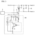
- Fig. 3 shows a conventional DC-DC converter circuit.
- reference numeral 1 indicates a transformer
- reference numeral 2 indicates a main switching element
- reference numeral 7 indicates an auxiliary output voltage circuit for smoothing the voltage at an auxiliary winding of the primary winding side of the transformer 1
- reference numeral 105 indicates a voltage measuring circuit. That is, this DC-DC converter circuit has a switching circuit which includes the main switching element 2 serially connected to the primary winding of the transformer 1, in which the primary winding side and the secondary winding side are insulated from each other. In this DC-DC converter circuit, the output voltage of the secondary side (i.e., the output side) is stabilized by performing PWM (pulse width modulation) control of the main switching element 2.
- PWM pulse width modulation
- the voltage measuring circuit 105 is provided for measuring the output voltage of the auxiliary output voltage circuit 7, which is output by smoothing the auxiliary winding voltage of the transformer 1, where the auxiliary winding voltage is in proportion to the output voltage of the secondary side.
- the measured level varies, particularly according to variation in the input voltage (i.e., Vin), so that an error is produced between the measured state and the actual state at the secondary side, thereby requiring an additional correction circuit.
- an inverter circuit for inverting the measured input voltage value obtained by resistance voltage division of the input voltage, or the like
- Such an inverter circuit is a complicated circuit employing a semiconductor which functions as an operational amplifier or the like, thereby producing problems such that the manufacturing cost is high, the area necessary for mounting such a complicated circuit is large, and the like.
- the limiting value for the output current at the secondary side is corrected so that the value is fixed, independent of variation in the input voltage at the primary side. More specifically, the input voltage is divided and the divided voltage is varied by a variable voltage generation circuit, and this voltage is provided as a comparative reference voltage to a comparison circuit, so that a control variable, which is in inverse proportion to the input voltage, is obtained so as to correct the measured current value (refer to Japanese Unexamined Patent Application, First Publication No. Hei 11-252908 (see Figs. 1 and 2), etc.).
- the structure of the variable voltage generation circuit is complicated and a comparative circuit is necessary; thus, the number of necessary parts is large.
- an object of the present invention is to provide a novel DC-DC converter circuit for stabilizing the output voltage of the secondary side by correcting the input voltage by using a simple circuit, where no state measurement circuit is necessary at the secondary side.
- the present invention provides a DC-DC converter circuit comprising:
- the correction circuit includes a resistor and a capacitor which are connected in series, and the resistor is connected to the driving circuit.
- the DC-DC converter circuit may further comprise a state measurement circuit, provided in the primary side, for detecting a state of the secondary side at the primary side, wherein the state measurement circuit is connected to the correction circuit.
- the transformer has an auxiliary winding provided at the primary side; and the state measurement circuit is an output voltage measuring circuit for indirectly measuring a smoothed voltage of the auxiliary winding as a voltage level of the output voltage of the secondary side, wherein the smoothed voltage of the auxiliary winding is in proportion to the output voltage of the secondary side.
- the state measurement circuit is a current measuring circuit for indirectly measuring an output current of the secondary side by measuring an input current of the primary side.
- the driving circuit for generating the PWM driving pulses is provided, and an output of the driving circuit is connected to the control terminal of the main switching element, and the correction circuit for outputting a voltage whose level is in inverse proportion to the input voltage is provided. Therefore, according to a smoothed voltage of the PWM driving pulses generated by the driving circuit (which is connected to the main switching element), correction in inverse proportion to the input voltage can be performed for a value measured by a state measurement circuit. Therefore, the output voltage of the secondary side can be stabilized by correcting the input voltage by using a simple circuit, where no state measurement circuit is necessary at the secondary side.
- the present invention can be applied to correction in indirect output-voltage control, measurement of overvoltage or overcurrent, and the like.
- Figs. 1 and 2 show embodiments of the DC-DC converter circuit of the present invention.
- reference numeral 1 indicates a transformer
- reference numeral 2 indicates a main switching element
- reference numeral 3 indicates a driving circuit
- reference numeral 4 indicates a correction circuit
- reference numeral 5 indicates a voltage measuring circuit
- reference numeral 6 indicates a current measuring circuit
- reference numeral 7 indicates an auxiliary output voltage circuit
- reference numeral 8 indicates a voltage measuring circuit
- reference numeral 9 indicates a comparison circuit.
- the DC-DC converter circuit shown in Fig. 1 has a circuit for measuring the output voltage of the secondary side by using a voltage obtained by smoothing the voltage of the auxiliary winding of the primary winding side.
- This DC-DC converter circuit has a switching circuit in which the main switching element 2, which employs a MOSFET (metal oxide semiconductor FET), is serially connected to the primary winding of the transformer 1, and a rectifying element 21, an output choke (coil) 22, and a smoothing capacitor 23 are provided at the secondary side, where the primary winding side and the secondary winding side of the transformer 1 are insulated from each other.
- PWM control of the main switching element 2 is performed so as to stabilize the output voltage of the secondary side.
- the driving circuit 3 for generating PWM driving pulses is provided, and the output of this driving circuit 3 is connected to the gate of the main switching element 2, and the voltage measuring circuit 5 is connected to the driving circuit 3.
- This voltage measuring circuit 5 has the correction circuit 4 for producing a voltage which is in inverse proportion to the input voltage (see Vin in Fig. 1), and also has the auxiliary output voltage circuit 7.
- the output of the driving circuit 3 is also connected to the correction circuit 4.
- the auxiliary output voltage circuit 7 is provided for smoothing the pulse voltage, which is produced at the auxiliary winding provided at the transformer 1, and outputting the smoothed voltage.
- the correction circuit 4 has a resistor 11 and a capacitor 12, which are connected in series, and the resistor 11 is connected to the driving circuit 3.
- the voltage measuring circuit 8 consisting of two serially-connected resistors, is connected to a connection point between the resistor 11 and the capacitor 12, and the auxiliary output voltage circuit 7 is connected to the voltage measuring circuit 8.
- the auxiliary output voltage circuit 7 has a rectifying element 13, an output choke 14, and a smoothing capacitor 15, and the voltage at the auxiliary winding is smoothed by a filter of the output choke 14 and the smoothing capacitor 15, so that the ratio of the output voltage of the switching circuit to the output voltage of the auxiliary output voltage circuit 7 is proportional to the winding ratio of the secondary winding to the auxiliary winding.
- the auxiliary output voltage circuit 7 is connected to the voltage measuring circuit 8; thus, the level of the auxiliary winding voltage, which has been smoothed by the auxiliary output voltage circuit 7, can be measured by the voltage measuring circuit 8.
- the DC-DC converter circuit of the present embodiment also has the comparison circuit 9 for comparing the auxiliary winding voltage with a reference voltage.
- the output of the voltage measuring circuit 8 is connected to the negative input of the comparison circuit 9 and a power source for providing the reference voltage is connected to the positive input of the comparison circuit 9.
- a driving pulse signal which is PWM-controlled, is sent from the driving circuit 3 to the main switching element 2.
- the main switching element 2 is alternately turned on and off, and current flows through the primary winding of the transformer 1. With the current flow through the primary side, current also flows through the secondary winding and the auxiliary winding of the transformer 1.
- the PWM-controlled driving pulse signal from the driving circuit 3 is also sent to the correction circuit 4. This signal sent to the correction circuit 4 is charged via the resistor 11 to the capacitor 12 of the correction circuit 4.
- the output voltage of the auxiliary output voltage circuit 7 is constant (independent of the input voltage) unless the output voltage at the secondary side is changed, and the output voltage of the auxiliary output voltage circuit 7 follows the variation at the secondary side.
- the value of the input current varies according to the variation in the input voltage, variation such as line drop (i.e., voltage drop) is produced, and the "on" width of the main switching element varies according to variation in the power efficiency, so that even when the output voltage at the secondary side is constant, the auxiliary winding voltage at the primary side varies according to the input voltage.
- the auxiliary winding voltage is in proportion to the variation in the input voltage, an error occurs between the actual output voltage at the secondary side and the indirectly measured voltage at the primary side if the measurement level of the voltage measuring circuit 5 for detecting the auxiliary winding voltage is not corrected.
- the output voltage of the correction circuit 4 decreases, and the output voltage of the auxiliary output voltage circuit 7, which is in proportion to the input voltage, is corrected via the outputs of the voltage measuring circuit 8 and the correction circuit 4, so that the input level at the negative side of the comparison circuit 9 can be constant.
- the DC-DC converter circuit shown in Fig. 2 has a circuit for indirectly measuring the output current of the secondary side by measuring the peak current at the primary side and a circuit for performing overcurrent protection.
- This DC-DC converter circuit has a switching circuit in which the main switching element 2, which employs a MOSFET, is serially connected to the primary winding of the transformer 1, and a rectifying element 21, an output choke 22, and a smoothing capacitor 23 are provided at the secondary side, where the primary winding side and the secondary winding side of the transformer 1 are insulated from each other.
- PWM control of the main switching element 2 is performed so as to stabilize the output voltage of the secondary side.
- the driving circuit 3 for generating PWM driving pulses is provided, and the output of this driving circuit 3 is connected to the gate of the main switching element 2, and the overcurrent measuring circuit 6 is connected to the driving circuit 3.
- This overcurrent measuring circuit 6 has the correction circuit 4.
- the correction circuit 4 has a resistor 11 and a capacitor 12, which are connected in series, and the resistor 11 is connected to the driving circuit 3.
- the voltage measuring circuit 8 is connected to a connection point between the resistor 11 and the capacitor 12, and this voltage measuring circuit 8 is also connected to the source of the main switching element 2.
- a current detecting resistor 16 is also connected to the source of the main switching element 2.
- the DC-DC converter circuit of the present embodiment also has the comparison circuit 9 for comparing the peak current level at the primary side with a reference voltage, where the peak current level has been converted into a corresponding voltage.
- the output of the voltage measuring circuit 8 is connected to the negative input of the comparison circuit 9 and a power source for providing the reference voltage is connected to the positive input of the comparison circuit 9.
- a driving pulse signal which is PWM-controlled, is sent from the driving circuit 3 to the main switching element 2.
- the main switching element 2 is alternately turned on and off, and current flows through the primary winding of the transformer 1. With the current flow through the primary side, current also flows through the secondary winding of the transformer 1.
- the PWM-controlled driving pulse signal from the driving circuit 3 is also sent to the correction circuit 4. This signal sent to the correction circuit 4 is charged via the resistor 11 to the capacitor 12 of the correction circuit 4.
- the output voltage of the correction circuit 4 decreases, and the voltage level converted from the peak current value of the primary side, which is in proportion to the input voltage, is corrected via the outputs of the voltage measuring circuit 8 and the correction circuit 4, so that the input level at the negative side of the comparison circuit 9 can be constant.
Landscapes
- Engineering & Computer Science (AREA)
- Power Engineering (AREA)
- Dc-Dc Converters (AREA)
Abstract
Description
- The present invention relates to a DC-DC converter circuit in which the primary winding side and the secondary winding side of a transformer are insulated from each other, and the primary side of the DC-DC converter circuit has a circuit for correcting the input voltage.
- Fig. 3 shows a conventional DC-DC converter circuit. In the figure, reference numeral 1 indicates a transformer,
reference numeral 2 indicates a main switching element,reference numeral 7 indicates an auxiliary output voltage circuit for smoothing the voltage at an auxiliary winding of the primary winding side of the transformer 1, andreference numeral 105 indicates a voltage measuring circuit. That is, this DC-DC converter circuit has a switching circuit which includes themain switching element 2 serially connected to the primary winding of the transformer 1, in which the primary winding side and the secondary winding side are insulated from each other. In this DC-DC converter circuit, the output voltage of the secondary side (i.e., the output side) is stabilized by performing PWM (pulse width modulation) control of themain switching element 2. Additionally, in order to indirectly measure the voltage of the secondary side at the primary side, thevoltage measuring circuit 105 is provided for measuring the output voltage of the auxiliaryoutput voltage circuit 7, which is output by smoothing the auxiliary winding voltage of the transformer 1, where the auxiliary winding voltage is in proportion to the output voltage of the secondary side. - However, in such an indirect measurement by measuring a state of the primary side, the measured level varies, particularly according to variation in the input voltage (i.e., Vin), so that an error is produced between the measured state and the actual state at the secondary side, thereby requiring an additional correction circuit. If variation in the measured level is in inverse proportion to the input voltage, an inverter circuit for inverting the measured input voltage value (obtained by resistance voltage division of the input voltage, or the like) is required as the auxiliary circuit. Such an inverter circuit is a complicated circuit employing a semiconductor which functions as an operational amplifier or the like, thereby producing problems such that the manufacturing cost is high, the area necessary for mounting such a complicated circuit is large, and the like.
- On the other hand, in a known correction method used for a power supply which performs stabilization control of the output voltage of the secondary side by controlling the current at the primary side of the transformer, the limiting value for the output current at the secondary side is corrected so that the value is fixed, independent of variation in the input voltage at the primary side. More specifically, the input voltage is divided and the divided voltage is varied by a variable voltage generation circuit, and this voltage is provided as a comparative reference voltage to a comparison circuit, so that a control variable, which is in inverse proportion to the input voltage, is obtained so as to correct the measured current value (refer to Japanese Unexamined Patent Application, First Publication No. Hei 11-252908 (see Figs. 1 and 2), etc.).
- In the above-explained DC-DC converter circuit, the structure of the variable voltage generation circuit is complicated and a comparative circuit is necessary; thus, the number of necessary parts is large.
- In consideration of the above circumstances, an object of the present invention is to provide a novel DC-DC converter circuit for stabilizing the output voltage of the secondary side by correcting the input voltage by using a simple circuit, where no state measurement circuit is necessary at the secondary side.
- Therefore, the present invention provides a DC-DC converter circuit comprising:
- a transformer having a primary winding and a secondary winding, wherein a primary side including the primary winding and a secondary side including the secondary winding are insulated from each other in the DC-DC converter circuit;
- a switching circuit including a main switching element which is connected to the primary winding in series and has a control terminal for controlling the main switching element, wherein the main switching element is PWM-controlled so as to stabilize an output voltage of the secondary side;
- a driving circuit for generating PWM driving pulses; and
- a correction circuit for outputting a voltage whose level is in inverse proportion to an input voltage of the DC-DC converter circuit, wherein an output of the driving circuit is connected to the control terminal of the main switching element and to the correction circuit.
-
- In a typical example, the correction circuit includes a resistor and a capacitor which are connected in series, and the resistor is connected to the driving circuit.
- The DC-DC converter circuit may further comprise a state measurement circuit, provided in the primary side, for detecting a state of the secondary side at the primary side, wherein the state measurement circuit is connected to the correction circuit.
- In this case, in a typical example, the transformer has an auxiliary winding provided at the primary side; and the state measurement circuit is an output voltage measuring circuit for indirectly measuring a smoothed voltage of the auxiliary winding as a voltage level of the output voltage of the secondary side, wherein the smoothed voltage of the auxiliary winding is in proportion to the output voltage of the secondary side.
- In another typical example, the state measurement circuit is a current measuring circuit for indirectly measuring an output current of the secondary side by measuring an input current of the primary side.
- In the present invention, the driving circuit for generating the PWM driving pulses is provided, and an output of the driving circuit is connected to the control terminal of the main switching element, and the correction circuit for outputting a voltage whose level is in inverse proportion to the input voltage is provided. Therefore, according to a smoothed voltage of the PWM driving pulses generated by the driving circuit (which is connected to the main switching element), correction in inverse proportion to the input voltage can be performed for a value measured by a state measurement circuit. Therefore, the output voltage of the secondary side can be stabilized by correcting the input voltage by using a simple circuit, where no state measurement circuit is necessary at the secondary side. In addition, the present invention can be applied to correction in indirect output-voltage control, measurement of overvoltage or overcurrent, and the like.
-
- Fig. 1 is a circuit diagram showing the structure of an embodiment of the DC-DC converter circuit according to the present invention.
- Fig. 2 is a circuit diagram showing the structure of another embodiment of the DC-DC converter circuit according to the present invention.
- Fig. 3 is a circuit diagram showing the structure of a conventional DC-DC converter circuit.
-
- Hereinafter, embodiments of the DC-DC converter circuit according to the present invention will be explained with reference to the drawings. Figs. 1 and 2 show embodiments of the DC-DC converter circuit of the present invention. In the figures, reference numeral 1 indicates a transformer,
reference numeral 2 indicates a main switching element,reference numeral 3 indicates a driving circuit, reference numeral 4 indicates a correction circuit,reference numeral 5 indicates a voltage measuring circuit,reference numeral 6 indicates a current measuring circuit,reference numeral 7 indicates an auxiliary output voltage circuit, reference numeral 8 indicates a voltage measuring circuit, andreference numeral 9 indicates a comparison circuit. - The DC-DC converter circuit shown in Fig. 1 has a circuit for measuring the output voltage of the secondary side by using a voltage obtained by smoothing the voltage of the auxiliary winding of the primary winding side. This DC-DC converter circuit has a switching circuit in which the
main switching element 2, which employs a MOSFET (metal oxide semiconductor FET), is serially connected to the primary winding of the transformer 1, and a rectifyingelement 21, an output choke (coil) 22, and asmoothing capacitor 23 are provided at the secondary side, where the primary winding side and the secondary winding side of the transformer 1 are insulated from each other. In this structure, PWM control of themain switching element 2 is performed so as to stabilize the output voltage of the secondary side. Here, thedriving circuit 3 for generating PWM driving pulses is provided, and the output of thisdriving circuit 3 is connected to the gate of themain switching element 2, and thevoltage measuring circuit 5 is connected to thedriving circuit 3. Thisvoltage measuring circuit 5 has the correction circuit 4 for producing a voltage which is in inverse proportion to the input voltage (see Vin in Fig. 1), and also has the auxiliaryoutput voltage circuit 7. The output of thedriving circuit 3 is also connected to the correction circuit 4. The auxiliaryoutput voltage circuit 7 is provided for smoothing the pulse voltage, which is produced at the auxiliary winding provided at the transformer 1, and outputting the smoothed voltage. - The correction circuit 4 has a
resistor 11 and acapacitor 12, which are connected in series, and theresistor 11 is connected to thedriving circuit 3. The voltage measuring circuit 8, consisting of two serially-connected resistors, is connected to a connection point between theresistor 11 and thecapacitor 12, and the auxiliaryoutput voltage circuit 7 is connected to the voltage measuring circuit 8. - Similar to the secondary side of the switching circuit, the auxiliary
output voltage circuit 7 has a rectifyingelement 13, anoutput choke 14, and asmoothing capacitor 15, and the voltage at the auxiliary winding is smoothed by a filter of theoutput choke 14 and thesmoothing capacitor 15, so that the ratio of the output voltage of the switching circuit to the output voltage of the auxiliaryoutput voltage circuit 7 is proportional to the winding ratio of the secondary winding to the auxiliary winding. - In addition, the auxiliary
output voltage circuit 7 is connected to the voltage measuring circuit 8; thus, the level of the auxiliary winding voltage, which has been smoothed by the auxiliaryoutput voltage circuit 7, can be measured by the voltage measuring circuit 8. The DC-DC converter circuit of the present embodiment also has thecomparison circuit 9 for comparing the auxiliary winding voltage with a reference voltage. The output of the voltage measuring circuit 8 is connected to the negative input of thecomparison circuit 9 and a power source for providing the reference voltage is connected to the positive input of thecomparison circuit 9. - The operation of the DC-DC converter circuit having the above-explained structure will be explained below. A driving pulse signal, which is PWM-controlled, is sent from the
driving circuit 3 to themain switching element 2. Themain switching element 2 is alternately turned on and off, and current flows through the primary winding of the transformer 1. With the current flow through the primary side, current also flows through the secondary winding and the auxiliary winding of the transformer 1. The PWM-controlled driving pulse signal from thedriving circuit 3 is also sent to the correction circuit 4. This signal sent to the correction circuit 4 is charged via theresistor 11 to thecapacitor 12 of the correction circuit 4. As a result, when the signal from thedriving circuit 3 is set to an on-state, the voltage of the correction circuit 4 gradually increases, and when the signal from thedriving circuit 3 is set to an off-state, thecapacitor 12 is discharged, so that the voltage of the correction circuit 4 gradually decreases. - Such increase and decrease of the voltage are alternately repeated, so that the output voltage of the correction circuit 4 has a waveform close to the average of the pulse signal from the
driving circuit 3. When the PWM control is performed, the higher the input voltage (i.e., Vin), the shorter the "on" time of the pulse signal of thedriving circuit 3. Conversely, the lower the input voltage, the longer the "on" time of the pulse signal of thedriving circuit 3. That is, when the input voltage is higher, the averaged voltage is lower, and conversely, and when the input voltage is lower, the averaged voltage is higher; thus, the output voltage of the correction circuit 4 is in inverse proportion to the input voltage. - Ideally, the output voltage of the auxiliary
output voltage circuit 7 is constant (independent of the input voltage) unless the output voltage at the secondary side is changed, and the output voltage of the auxiliaryoutput voltage circuit 7 follows the variation at the secondary side. However, actually, the value of the input current varies according to the variation in the input voltage, variation such as line drop (i.e., voltage drop) is produced, and the "on" width of the main switching element varies according to variation in the power efficiency, so that even when the output voltage at the secondary side is constant, the auxiliary winding voltage at the primary side varies according to the input voltage. When the auxiliary winding voltage is in proportion to the variation in the input voltage, an error occurs between the actual output voltage at the secondary side and the indirectly measured voltage at the primary side if the measurement level of the voltage measuringcircuit 5 for detecting the auxiliary winding voltage is not corrected. - In the present embodiment, when the input voltage increases, the output voltage of the correction circuit 4 decreases, and the output voltage of the auxiliary
output voltage circuit 7, which is in proportion to the input voltage, is corrected via the outputs of the voltage measuring circuit 8 and the correction circuit 4, so that the input level at the negative side of thecomparison circuit 9 can be constant. - The DC-DC converter circuit shown in Fig. 2 has a circuit for indirectly measuring the output current of the secondary side by measuring the peak current at the primary side and a circuit for performing overcurrent protection.
- This DC-DC converter circuit has a switching circuit in which the
main switching element 2, which employs a MOSFET, is serially connected to the primary winding of the transformer 1, and a rectifyingelement 21, anoutput choke 22, and a smoothingcapacitor 23 are provided at the secondary side, where the primary winding side and the secondary winding side of the transformer 1 are insulated from each other. In this structure, PWM control of themain switching element 2 is performed so as to stabilize the output voltage of the secondary side. Here, the drivingcircuit 3 for generating PWM driving pulses is provided, and the output of thisdriving circuit 3 is connected to the gate of themain switching element 2, and theovercurrent measuring circuit 6 is connected to thedriving circuit 3. Thisovercurrent measuring circuit 6 has the correction circuit 4. - The correction circuit 4 has a
resistor 11 and acapacitor 12, which are connected in series, and theresistor 11 is connected to thedriving circuit 3. The voltage measuring circuit 8 is connected to a connection point between theresistor 11 and thecapacitor 12, and this voltage measuring circuit 8 is also connected to the source of themain switching element 2. A current detectingresistor 16 is also connected to the source of themain switching element 2. The DC-DC converter circuit of the present embodiment also has thecomparison circuit 9 for comparing the peak current level at the primary side with a reference voltage, where the peak current level has been converted into a corresponding voltage. The output of the voltage measuring circuit 8 is connected to the negative input of thecomparison circuit 9 and a power source for providing the reference voltage is connected to the positive input of thecomparison circuit 9. - The operation of the DC-DC converter circuit having the above-explained structure will be explained below. A driving pulse signal, which is PWM-controlled, is sent from the driving
circuit 3 to themain switching element 2. Themain switching element 2 is alternately turned on and off, and current flows through the primary winding of the transformer 1. With the current flow through the primary side, current also flows through the secondary winding of the transformer 1. The PWM-controlled driving pulse signal from the drivingcircuit 3 is also sent to the correction circuit 4. This signal sent to the correction circuit 4 is charged via theresistor 11 to thecapacitor 12 of the correction circuit 4. As a result, when the signal from the drivingcircuit 3 is set to the on-state, the voltage of the correction circuit gradually increases, and when the signal from the drivingcircuit 3 is set to the off-state, thecapacitor 12 is discharged, so that the voltage of the correction circuit gradually decreases. - Such increase and decrease of the voltage are alternately repeated, so that the output voltage of the correction circuit 4 has a waveform close to the average of the pulse signal from the driving
circuit 3. When the PWM control is performed, the higher the input voltage, the shorter the "on" time of the pulse signal of the drivingcircuit 3. Conversely, the lower the input voltage, the longer the "on" time of the pulse signal of the drivingcircuit 3. That is, when the input voltage is higher, the averaged voltage is lower, and conversely, when the input voltage is lower, the averaged voltage is higher; thus, the output voltage of the correction circuit 4 is in inverse proportion to the input voltage. However, when the current at the secondary side is constant, the current flowing through the primary winding is in proportion to the input voltage. Therefore, the measurement level of theovercurrent measuring circuit 6 varies depending on the input voltage, so that an error occurs between the output current value at the secondary side and the indirectly measured current value. - In the present embodiment, when the input voltage increases, the output voltage of the correction circuit 4 decreases, and the voltage level converted from the peak current value of the primary side, which is in proportion to the input voltage, is corrected via the outputs of the voltage measuring circuit 8 and the correction circuit 4, so that the input level at the negative side of the
comparison circuit 9 can be constant. - While preferred embodiments of the invention have been described and illustrated above, it should be understood that these are exemplary of the invention and are not to be considered as limiting. Additions, omissions, substitutions, and other modifications can be made without departing from the spirit or scope of the present invention. Accordingly, the invention is not to be considered as being limited by the foregoing description, and is only limited by the scope of the appended claims.
Claims (8)
- A DC-DC converter circuit comprising:wherein an output of the driving circuit is connected to the control terminal of the main switching element and to the correction circuit.a transformer (1) having a primary winding and a secondary winding, wherein a primary side including the primary winding and a secondary side including the secondary winding are insulated from each other in the DC-DC converter circuit;a switching circuit including a main switching element (2) which is connected to the primary winding in series and has a control terminal for controlling the main switching element, wherein the main switching element is PWM-controlled so as to stabilize an output voltage of the secondary side;a driving circuit (3) for generating PWM driving pulses; anda correction circuit (4) for outputting a voltage whose level is in inverse proportion to an input voltage of the DC-DC converter circuit,
- A DC-DC converter circuit as claimed in claim 1, wherein the correction circuit includes a resistor (11) and a capacitor (12) which are connected in series, and the resistor is connected to the driving circuit.
- A DC-DC converter circuit as claimed in claim 1, further comprising:a state measurement circuit (5; 6), provided in the primary side, for detecting a state of the secondary side at the primary side, wherein the state measurement circuit is connected to the correction circuit.
- A DC-DC converter circuit as claimed in claim 2, further comprising:a state measurement circuit (5; 6), provided in the primary side, for detecting a state of the secondary side at the primary side, wherein the state measurement circuit is connected to the correction circuit.
- A DC-DC converter circuit as claimed in claim 3, wherein:the transformer has an auxiliary winding provided at the primary side; andthe state measurement circuit is an output voltage measuring circuit (5) for indirectly measuring a smoothed voltage of the auxiliary winding as a voltage level of the output voltage of the secondary side, wherein the smoothed voltage of the auxiliary winding is in proportion to the output voltage of the secondary side.
- A DC-DC converter circuit as claimed in claim 4, wherein:the transformer has an auxiliary winding provided at the primary side; andthe state measurement circuit is an output voltage measuring circuit (5) for indirectly measuring a smoothed voltage of the auxiliary winding as a voltage level of the output voltage of the secondary side, wherein the smoothed voltage of the auxiliary winding is in proportion to the output voltage of the secondary side.
- A DC-DC converter circuit as claimed in claim 3, wherein the state measurement circuit is a current measuring circuit (6) for indirectly measuring an output current of the secondary side by measuring an input current of the primary side.
- A DC-DC converter circuit as claimed in claim 4, wherein the state measurement circuit is a current measuring circuit (6) for indirectly measuring an output current of the secondary side by measuring an input current of the primary side.
Applications Claiming Priority (2)
| Application Number | Priority Date | Filing Date | Title |
|---|---|---|---|
| JP2002365191 | 2002-12-17 | ||
| JP2002365191A JP2004201385A (en) | 2002-12-17 | 2002-12-17 | Dc-dc converter circuit |
Publications (1)
| Publication Number | Publication Date |
|---|---|
| EP1432108A1 true EP1432108A1 (en) | 2004-06-23 |
Family
ID=32376242
Family Applications (1)
| Application Number | Title | Priority Date | Filing Date |
|---|---|---|---|
| EP03257622A Withdrawn EP1432108A1 (en) | 2002-12-17 | 2003-12-03 | DC-DC converter having input voltage compensating circuit |
Country Status (3)
| Country | Link |
|---|---|
| US (1) | US7006363B2 (en) |
| EP (1) | EP1432108A1 (en) |
| JP (1) | JP2004201385A (en) |
Cited By (6)
| Publication number | Priority date | Publication date | Assignee | Title |
|---|---|---|---|---|
| WO2008132512A1 (en) * | 2007-04-27 | 2008-11-06 | Cambridge Semiconductor Limited | Power converters |
| GB2450004A (en) * | 2006-05-26 | 2008-12-10 | Cambridge Semiconductor Ltd | Resonant discontinuous forward power converter |
| US7570497B2 (en) | 2006-05-26 | 2009-08-04 | Cambridge Semiconductor | Discontinuous quasi-resonant forward converter |
| US7738266B2 (en) | 2006-05-26 | 2010-06-15 | Cambridge Semiconductor Limited | Forward power converter controllers |
| CN102279304A (en) * | 2011-03-31 | 2011-12-14 | 欧瑞传动电气有限公司 | Direct current bus voltage detecting circuit for low voltage frequency converter |
| CN103229404A (en) * | 2010-04-29 | 2013-07-31 | 德州仪器(科克)有限公司 | Voltage sensing arrangement for a flyback converter |
Families Citing this family (10)
| Publication number | Priority date | Publication date | Assignee | Title |
|---|---|---|---|---|
| CN100433520C (en) * | 2005-03-04 | 2008-11-12 | 崇贸科技股份有限公司 | Switching type control device for primary side control output current of power supply |
| EP1918597A4 (en) * | 2005-08-25 | 2011-10-26 | Thk Co Ltd | Movement guiding device |
| US7359222B2 (en) * | 2005-09-15 | 2008-04-15 | Power Integrations, Inc. | Method and apparatus to improve regulation of a power supply |
| JP2007174890A (en) * | 2005-11-28 | 2007-07-05 | Matsushita Electric Ind Co Ltd | Switching power supply device and semiconductor device used therefor |
| EP2333944B1 (en) * | 2009-02-06 | 2018-12-19 | Shindengen Electric Manufacturing Co., Ltd. | Current detecting circuit and transformer current measuring system |
| JP5023400B2 (en) * | 2009-08-24 | 2012-09-12 | エヌイーシーコンピュータテクノ株式会社 | Power circuit |
| CN103036453A (en) * | 2011-10-10 | 2013-04-10 | 王熙宁 | Switching alternative current and direct current conversion circuit capable of reducing amplitude wave of output voltage |
| JP5862312B2 (en) * | 2012-01-11 | 2016-02-16 | 株式会社村田製作所 | Switching power supply |
| KR101398586B1 (en) * | 2012-12-18 | 2014-05-23 | 충북대학교 산학협력단 | 1/x circuit using capacitor charging time |
| CN104660049A (en) * | 2014-02-18 | 2015-05-27 | 襄阳南车电气系统技术有限公司 | DC-DC converter with input voltage compensating circuit |
Citations (5)
| Publication number | Priority date | Publication date | Assignee | Title |
|---|---|---|---|---|
| US4017782A (en) * | 1975-11-07 | 1977-04-12 | General Electric Company | DC-DC converter |
| DE4105463A1 (en) * | 1991-02-21 | 1992-08-27 | Siemens Ag | CONTROL METHOD FOR A VOLTAGE CONVERTER WITH A LARGE INPUT VOLTAGE RANGE AND USE OF SUCH A METHOD |
| US5430405A (en) * | 1992-08-12 | 1995-07-04 | Lambda Electronics Inc. | Control circuit for converters operating in the discontinuous mode |
| US5742494A (en) * | 1994-10-28 | 1998-04-21 | Siemens Aktiengesellschaft | Circuit arrangement for driving a converter |
| JPH11252908A (en) * | 1998-02-27 | 1999-09-17 | Hitachi Ltd | Voltage stabilizer |
Family Cites Families (1)
| Publication number | Priority date | Publication date | Assignee | Title |
|---|---|---|---|---|
| KR100226150B1 (en) * | 1997-07-11 | 1999-10-15 | 구자홍 | Boost-up power-factor correcting circuit by utilizing power feedback |
-
2002
- 2002-12-17 JP JP2002365191A patent/JP2004201385A/en active Pending
-
2003
- 2003-12-03 EP EP03257622A patent/EP1432108A1/en not_active Withdrawn
- 2003-12-12 US US10/733,339 patent/US7006363B2/en not_active Expired - Fee Related
Patent Citations (5)
| Publication number | Priority date | Publication date | Assignee | Title |
|---|---|---|---|---|
| US4017782A (en) * | 1975-11-07 | 1977-04-12 | General Electric Company | DC-DC converter |
| DE4105463A1 (en) * | 1991-02-21 | 1992-08-27 | Siemens Ag | CONTROL METHOD FOR A VOLTAGE CONVERTER WITH A LARGE INPUT VOLTAGE RANGE AND USE OF SUCH A METHOD |
| US5430405A (en) * | 1992-08-12 | 1995-07-04 | Lambda Electronics Inc. | Control circuit for converters operating in the discontinuous mode |
| US5742494A (en) * | 1994-10-28 | 1998-04-21 | Siemens Aktiengesellschaft | Circuit arrangement for driving a converter |
| JPH11252908A (en) * | 1998-02-27 | 1999-09-17 | Hitachi Ltd | Voltage stabilizer |
Non-Patent Citations (1)
| Title |
|---|
| PATENT ABSTRACTS OF JAPAN vol. 1999, no. 14 22 December 1999 (1999-12-22) * |
Cited By (10)
| Publication number | Priority date | Publication date | Assignee | Title |
|---|---|---|---|---|
| GB2450004A (en) * | 2006-05-26 | 2008-12-10 | Cambridge Semiconductor Ltd | Resonant discontinuous forward power converter |
| GB2456599A (en) * | 2006-05-26 | 2009-07-22 | Cambridge Semiconductor Ltd | Resonant discontinuous forward power converter |
| US7570497B2 (en) | 2006-05-26 | 2009-08-04 | Cambridge Semiconductor | Discontinuous quasi-resonant forward converter |
| GB2456599B (en) * | 2006-05-26 | 2009-12-02 | Cambridge Semiconductor Ltd | Forward power converters and controllers |
| GB2450004B (en) * | 2006-05-26 | 2010-02-10 | Cambridge Semiconductor Ltd | Forward power converters and controllers |
| US7738266B2 (en) | 2006-05-26 | 2010-06-15 | Cambridge Semiconductor Limited | Forward power converter controllers |
| WO2008132512A1 (en) * | 2007-04-27 | 2008-11-06 | Cambridge Semiconductor Limited | Power converters |
| CN103229404A (en) * | 2010-04-29 | 2013-07-31 | 德州仪器(科克)有限公司 | Voltage sensing arrangement for a flyback converter |
| CN103229404B (en) * | 2010-04-29 | 2017-07-21 | 德州仪器(科克)有限公司 | Arrangement is read for the voltage of flyback converter |
| CN102279304A (en) * | 2011-03-31 | 2011-12-14 | 欧瑞传动电气有限公司 | Direct current bus voltage detecting circuit for low voltage frequency converter |
Also Published As
| Publication number | Publication date |
|---|---|
| US7006363B2 (en) | 2006-02-28 |
| JP2004201385A (en) | 2004-07-15 |
| US20040120165A1 (en) | 2004-06-24 |
Similar Documents
| Publication | Publication Date | Title |
|---|---|---|
| US7006363B2 (en) | DC-DC converter circuit having correction circuit for outputting voltage level inversely proportional to input voltage | |
| US10104732B2 (en) | LED drive method and LED drive device | |
| US10673331B2 (en) | Circuit with reduced light load power dissipation and a method thereof | |
| JP6476997B2 (en) | Power supply control semiconductor device | |
| US20030026115A1 (en) | Switching-type DC-DC converter | |
| JP3961505B2 (en) | Voltage detection circuit, power supply device and semiconductor device | |
| TW201946351A (en) | Semiconductor device for power control, switching power device and design method thereof | |
| US20050162143A1 (en) | Power factor improving converter and control method thereof | |
| US6661684B2 (en) | AC-to-DC converter | |
| US8085007B2 (en) | Switching power supply circuit | |
| KR100622941B1 (en) | Switching power supply apparatus | |
| JP2006050724A (en) | Current detection circuit and switching power supply using the same | |
| US10090767B2 (en) | Switching power supply device having a pulse width holder | |
| CN108061580B (en) | Excitation circuit of electromagnetic flowmeter and electromagnetic flowmeter | |
| JP4104868B2 (en) | Switching power supply | |
| JP2888729B2 (en) | Output short circuit protection circuit | |
| JP5029056B2 (en) | Detection circuit and power supply system | |
| JP2006136146A (en) | Switching power supply | |
| JP4259119B2 (en) | Output power detection circuit and switching power supply device with output current detection function | |
| EP3745593A1 (en) | Method for driving a switch in a power converter, drive circuit and power converter | |
| TW200408179A (en) | Over-current protection apparatus and method of switching type regulator | |
| JP4214484B2 (en) | DC power supply | |
| JP4969204B2 (en) | Overcurrent protection circuit | |
| JP2003274648A (en) | Switching power unit | |
| JP4432115B2 (en) | Switching power supply |
Legal Events
| Date | Code | Title | Description |
|---|---|---|---|
| PUAI | Public reference made under article 153(3) epc to a published international application that has entered the european phase |
Free format text: ORIGINAL CODE: 0009012 |
|
| AK | Designated contracting states |
Kind code of ref document: A1 Designated state(s): AT BE BG CH CY CZ DE DK EE ES FI FR GB GR HU IE IT LI LU MC NL PT RO SE SI SK TR |
|
| AX | Request for extension of the european patent |
Extension state: AL LT LV MK |
|
| 17P | Request for examination filed |
Effective date: 20041125 |
|
| AKX | Designation fees paid |
Designated state(s): AT BE BG CH CY CZ DE DK EE ES FI FR GB GR HU IE IT LI LU MC NL PT RO SE SI SK TR |
|
| 17Q | First examination report despatched |
Effective date: 20071105 |
|
| GRAP | Despatch of communication of intention to grant a patent |
Free format text: ORIGINAL CODE: EPIDOSNIGR1 |
|
| STAA | Information on the status of an ep patent application or granted ep patent |
Free format text: STATUS: THE APPLICATION IS DEEMED TO BE WITHDRAWN |
|
| 18D | Application deemed to be withdrawn |
Effective date: 20081017 |