EP1432033A1 - Multi-chip module and method of forming - Google Patents
Multi-chip module and method of forming Download PDFInfo
- Publication number
- EP1432033A1 EP1432033A1 EP03078782A EP03078782A EP1432033A1 EP 1432033 A1 EP1432033 A1 EP 1432033A1 EP 03078782 A EP03078782 A EP 03078782A EP 03078782 A EP03078782 A EP 03078782A EP 1432033 A1 EP1432033 A1 EP 1432033A1
- Authority
- EP
- European Patent Office
- Prior art keywords
- laminate substrate
- package
- laminate
- substrate
- mounted device
- Prior art date
- Legal status (The legal status is an assumption and is not a legal conclusion. Google has not performed a legal analysis and makes no representation as to the accuracy of the status listed.)
- Granted
Links
Images

Classifications
-
- H—ELECTRICITY
- H10—SEMICONDUCTOR DEVICES; ELECTRIC SOLID-STATE DEVICES NOT OTHERWISE PROVIDED FOR
- H10W—GENERIC PACKAGES, INTERCONNECTIONS, CONNECTORS OR OTHER CONSTRUCTIONAL DETAILS OF DEVICES COVERED BY CLASS H10
- H10W74/00—Encapsulations, e.g. protective coatings
- H10W74/10—Encapsulations, e.g. protective coatings characterised by their shape or disposition
- H10W74/111—Encapsulations, e.g. protective coatings characterised by their shape or disposition the semiconductor body being completely enclosed
- H10W74/114—Encapsulations, e.g. protective coatings characterised by their shape or disposition the semiconductor body being completely enclosed by a substrate and the encapsulations
- H10W74/117—Encapsulations, e.g. protective coatings characterised by their shape or disposition the semiconductor body being completely enclosed by a substrate and the encapsulations the substrate having spherical bumps for external connection
-
- H—ELECTRICITY
- H10—SEMICONDUCTOR DEVICES; ELECTRIC SOLID-STATE DEVICES NOT OTHERWISE PROVIDED FOR
- H10W—GENERIC PACKAGES, INTERCONNECTIONS, CONNECTORS OR OTHER CONSTRUCTIONAL DETAILS OF DEVICES COVERED BY CLASS H10
- H10W70/00—Package substrates; Interposers; Redistribution layers [RDL]
- H10W70/60—Insulating or insulated package substrates; Interposers; Redistribution layers
- H10W70/611—Insulating or insulated package substrates; Interposers; Redistribution layers for connecting multiple chips together
-
- H—ELECTRICITY
- H10—SEMICONDUCTOR DEVICES; ELECTRIC SOLID-STATE DEVICES NOT OTHERWISE PROVIDED FOR
- H10W—GENERIC PACKAGES, INTERCONNECTIONS, CONNECTORS OR OTHER CONSTRUCTIONAL DETAILS OF DEVICES COVERED BY CLASS H10
- H10W74/00—Encapsulations, e.g. protective coatings
- H10W74/01—Manufacture or treatment
-
- H—ELECTRICITY
- H10—SEMICONDUCTOR DEVICES; ELECTRIC SOLID-STATE DEVICES NOT OTHERWISE PROVIDED FOR
- H10W—GENERIC PACKAGES, INTERCONNECTIONS, CONNECTORS OR OTHER CONSTRUCTIONAL DETAILS OF DEVICES COVERED BY CLASS H10
- H10W90/00—Package configurations
- H10W90/401—Package configurations characterised by multiple insulating or insulated package substrates, interposers or RDLs
-
- H—ELECTRICITY
- H10—SEMICONDUCTOR DEVICES; ELECTRIC SOLID-STATE DEVICES NOT OTHERWISE PROVIDED FOR
- H10W—GENERIC PACKAGES, INTERCONNECTIONS, CONNECTORS OR OTHER CONSTRUCTIONAL DETAILS OF DEVICES COVERED BY CLASS H10
- H10W74/00—Encapsulations, e.g. protective coatings
-
- H—ELECTRICITY
- H10—SEMICONDUCTOR DEVICES; ELECTRIC SOLID-STATE DEVICES NOT OTHERWISE PROVIDED FOR
- H10W—GENERIC PACKAGES, INTERCONNECTIONS, CONNECTORS OR OTHER CONSTRUCTIONAL DETAILS OF DEVICES COVERED BY CLASS H10
- H10W74/00—Encapsulations, e.g. protective coatings
- H10W74/10—Encapsulations, e.g. protective coatings characterised by their shape or disposition
- H10W74/15—Encapsulations, e.g. protective coatings characterised by their shape or disposition on active surfaces of flip-chip devices, e.g. underfills
-
- H—ELECTRICITY
- H10—SEMICONDUCTOR DEVICES; ELECTRIC SOLID-STATE DEVICES NOT OTHERWISE PROVIDED FOR
- H10W—GENERIC PACKAGES, INTERCONNECTIONS, CONNECTORS OR OTHER CONSTRUCTIONAL DETAILS OF DEVICES COVERED BY CLASS H10
- H10W90/00—Package configurations
-
- H—ELECTRICITY
- H10—SEMICONDUCTOR DEVICES; ELECTRIC SOLID-STATE DEVICES NOT OTHERWISE PROVIDED FOR
- H10W—GENERIC PACKAGES, INTERCONNECTIONS, CONNECTORS OR OTHER CONSTRUCTIONAL DETAILS OF DEVICES COVERED BY CLASS H10
- H10W90/00—Package configurations
- H10W90/701—Package configurations characterised by the relative positions of pads or connectors relative to package parts
- H10W90/751—Package configurations characterised by the relative positions of pads or connectors relative to package parts of bond wires
- H10W90/754—Package configurations characterised by the relative positions of pads or connectors relative to package parts of bond wires between a chip and a stacked insulating package substrate, interposer or RDL
Definitions
- the present invention generally relates to circuit device packages. More particularly, this invention relates to a multi-chip module (MCM) and method adapted to permit both underfilling and overmolding of surface-mounted devices on opposite surfaces of a laminate substrate within the MCM.
- MCM multi-chip module
- a flip chip is generally a surface-mounted (SM) device in the form of a monolithic semiconductor chip, such as an integrated circuit (IC) chip, having bead-like solder terminals formed on one of its surfaces.
- the terminals also referred to as solder bumps, serve to both secure the chip to a circuit board and electrically interconnect the flip chip circuitry to a conductor pattern formed on the circuit board, which may be a ceramic substrate, printed circuit board (PCB), printed wiring board (PWB), flexible circuit, or a silicon substrate.
- BGA ball grid array
- An example of a BGA package 110 is shown in Figure 1 as including an IC semiconductor chip 112 that is wire bonded to a substrate 114, e.g., a laminate PCB, with wires 116.
- the wires 116 are electrically connected through vias (not shown) in the substrate 114 to terminals 118 on the opposite surface of the substrate 114.
- the terminals 118 serve as interconnects between the chip 112 and a conductor pattern on a circuit board (not shown) to which the BGA package 110 will be mounted.
- Figure 2 is an example of the use of a flip chip 122 in a BGA package 120 to form a single-chip module.
- the flip chip 122 is equipped with solder bumps that form solder joint connections 126 when the chip 122 is flip-chip mounted to a conductor pattern on a substrate 124, e.g., a high-density PCB, which can then be mounted to a circuit (mother) board (not shown) with terminals 128 on the lower surface of the substrate 124.
- a substrate 124 e.g., a high-density PCB
- the substrate 124 is a PCB
- Figure 2 shows the interior of the BGA package 120 comprising a molding compound 132 that overmolds the chip 122.
- the present invention provides a package and packaging method that incorporate multiple surface-mounted devices, such as flip chips, mounted to a chip carrier, which in turn can be mounted onto a circuit board.
- the package is configured to provide a cost-effective, high-density multi-chip module that is also configured to facilitate underfilling and/or overmolding of circuit devices mounted on both sides of the chip carrier.
- the package of this invention generally includes a pair of laminate substrates that together form a chip carrier and input/output (I/O) interface structure for a number of chips, e.g., flip chips, wire-bonded chips and/or other surface-mount components.
- a first of the laminate substrates has a first conductor pattern on a first surface thereof and a second conductor pattern on an oppositely-disposed second surface thereof.
- the second laminate substrate is attached to the first laminate substrate, and has an interior opening therethrough that is surrounded by a frame portion.
- the frame portion has a first surface facing the first laminate substrate and an oppositely-disposed second surface on which solder terminals are present.
- One or more surface-mounted devices are mounted to each of the first and second surfaces of the first laminate substrate.
- the first and second laminate substrates are attached to each other such that the surface-mounted device mounted to the second surface of the first laminate substrate is disposed within the interior opening of the second laminate substrate.
- the present invention provides a process for forming an MCM package in which one or more surface-mounted devices are located within a cavity defined by the interior opening in the second laminate substrate.
- the second laminate substrate is preferably configured with lateral openings, preferably located in its first surface and therefore between the first and second laminate substrates. Through one of these lateral openings, a molding compound can be injected into the cavity defined by the interior opening in the second laminate substrate, with the result that the device mounted to the second surface of the first laminate substrate can be simultaneously underfilled and overmolded.
- the present invention provides a dual-sided MCM package that can be equipped with flip chips on opposite surfaces of a laminate substrate. Advantages include a relatively lowcost, electrically testable package whose surface-mounted devices can readily be both underfilled and overmolded to promote the reliability of the package.
- a flip-chip package 10 in accordance with this invention is represented in cross-section in Figure 3.
- the package 10 includes a pair of laminate PCB's 12 and 14 that are secured together to form a unitary chip carrier and input/output (I/O) interface structure for a number of flip chips 16 mounted to both surfaces of one of the PCB's 12.
- the package 10 can be termed a dual-sided flip-chip MCM BGA package. While flip chips 16 are illustrated in the Figures, various types of circuit components could be present in the package 10 in addition to or in place of the flip chips 16, for example, wire-bonded chips and/or other surface-mount components.
- the upper PCB 12 (as viewed in Figure 3) is shown as a multilayer laminate substrate, though other types of substrates could foreseeably be used.
- the flip chips 16 are mounted to opposite surfaces 18 and 20 of the PCB 12, as can be other surface-mounted (SM) components, such that the PCB 12 will be referred to as the carrier PCB 12.
- the chips 16 are physically and electrically connected to conductor patterns on the chip carrier PCB 12 with solder joint connections 22 formed by reflowing solder bumps on the chips 16.
- the second PCB 14 is depicted as a two-layer laminate substrate, though again other substrate configurations are within the scope of this invention.
- One surface 24 of the PCB 14 faces the carrier PCB 12, while the opposite surface 26 is equipped with solder balls 28 attached to bond pads 30, through which I/O signals from the chips 16 can be communicated with a mother board (not shown) to which the package 10 is eventually mounted.
- the PCB 14 will be referred to as the I/O PCB 14.
- the I/O PCB 14 can be attached to the carrier PCB 12 by a suitable method that allows electrical interconnection between the two PCB's 12 and 14.
- the PCB's 12 and 14 may be attached at the manufacturing level, or in a subsequent operation with a conductive adhesive or, as represented in Figure 3, solder 32. Whatever the attachment method, electrical paths must be provided between the flip chip connections 22 and the solder balls 28, such as through metallized vias 56 through the I/O PCB 14.
- the I/O PCB 14 is fabricated to have an interior opening 38, with the remainder of the PCB 14 defining a frame 40 that surrounds the opening 38.
- the opening 38 and frame 40 are illustrated as having rectangular shapes, though other shapes could be employed.
- the opening 38 in the I/O PCB 14 defines a cavity 42 in which are contained the flip chips 16 attached to the lower surface 20 of the carrier PCB 12.
- the cavity 42 contains a compound 44 that encapsulate the flip chips 16 attached to the lower surface 20 of the carrier PCB 12.
- the package 10 is equipped with a gate 46 and vent 48 through which a suitable polymeric material can be injected into the cavity 42 to form the compound 44.
- the gate 46 and vent 48 are represented in Figures 3 through 5 as being formed by removing material from the surface 24 of the I/O PCB 14, preferably at two opposing corners of the PCB 14.
- the I/O PCB 14 is shown as having two slots 50 and 52 milled in its surface 24, the wider slot 50 corresponding to the gate 46 and the narrower slot 52 corresponding to the vent 48.
- the slots 50 and 52 extend diagonally from opposite corners of the opening 38 to the outer peripheral edge of the I/O PCB 14.
- a film-assisted molding (FAME) technique is preferably utilized.
- FAME film-assisted molding
- a film 58 is applied to the lower surface 26 of the I/O PCB 14 prior to placement of the solder balls 28.
- a suitable liquid polymeric material such as a thermoset epoxy, is then injected with a nozzle 60 through the gate 46 and into the cavity 42, and is thereafter cured to form the compound 44.
- the same polymeric material can be simultaneously injected with the nozzle 60 onto the upper surface 18 of the carrier PCB 12 to form a mold compound 54 that, as shown in Figure 3, encapsulates and preferably underfills the chips 16 on the upper surface 18 of the PCB 12.
- the gaseous contents of the cavity 42 escape through the vent 48.
- Placement of the gate 46 and vent 48 at the package corners promotes the ability of the liquid polymeric material to completely fill the cavity 42 and reduces the occurrence of voids within the compound 44.
- An alternative approach is depicted in Figure 7, in which the gate 46 is replaced with at least one internal gate 64, shown in the form of a through-hole in the PCB 12.
- the polymeric material is injected with a nozzle 62 onto the upper surface 18 of the carrier PCB 12, and then flows downward into the cavity 42 through the internal gate 64.
- the gaseous contents of the cavity 42 escape through the vent 48 as the cavity 42 fills with the polymeric material.
- a liquid material can be injected into the cavity 42 to both underfill and overmold the chips 16 on the lower surface 20 of the carrier PCB 12, and can be simultaneously deposited on the upper surface 18 of the PCB 12 to encapsulate and underfill chips 16 on the upper surface 18.
- the resulting package 10 thus has all of its chips 16 (as well as any other devices mounted to the carrier PCB 12), mechanically protected from extraneous damage as well as underfilled to promote the reliability of their solder connections 22.
- the layouts of the PCB's 12 and 14 can be configured such that the package 10 can be molded in strip form, in which multiple packages 10 can be simultaneously molded in a single operation.
Landscapes
- Encapsulation Of And Coatings For Semiconductor Or Solid State Devices (AREA)
- Wire Bonding (AREA)
- Structures Or Materials For Encapsulating Or Coating Semiconductor Devices Or Solid State Devices (AREA)
Abstract
Description
- The present invention generally relates to circuit device packages. More particularly, this invention relates to a multi-chip module (MCM) and method adapted to permit both underfilling and overmolding of surface-mounted devices on opposite surfaces of a laminate substrate within the MCM.
- A flip chip is generally a surface-mounted (SM) device in the form of a monolithic semiconductor chip, such as an integrated circuit (IC) chip, having bead-like solder terminals formed on one of its surfaces. The terminals, also referred to as solder bumps, serve to both secure the chip to a circuit board and electrically interconnect the flip chip circuitry to a conductor pattern formed on the circuit board, which may be a ceramic substrate, printed circuit board (PCB), printed wiring board (PWB), flexible circuit, or a silicon substrate.
- While typically mounted directly to a substrate, flip chips have been incorporated into packages, an example of which is ball grid array (BGA) packages. An example of a
BGA package 110 is shown in Figure 1 as including anIC semiconductor chip 112 that is wire bonded to asubstrate 114, e.g., a laminate PCB, withwires 116. Thewires 116 are electrically connected through vias (not shown) in thesubstrate 114 toterminals 118 on the opposite surface of thesubstrate 114. Similar to the flip-chip process, theterminals 118 serve as interconnects between thechip 112 and a conductor pattern on a circuit board (not shown) to which theBGA package 110 will be mounted. Figure 2 is an example of the use of aflip chip 122 in aBGA package 120 to form a single-chip module. Theflip chip 122 is equipped with solder bumps that form solderjoint connections 126 when thechip 122 is flip-chip mounted to a conductor pattern on asubstrate 124, e.g., a high-density PCB, which can then be mounted to a circuit (mother) board (not shown) withterminals 128 on the lower surface of thesubstrate 124. In the case where thesubstrate 124 is a PCB, it is desirable to underfill theflip chip 122 with a filledepoxy 130 to ensure the reliability of the solderjoint connections 126. Finally, Figure 2 shows the interior of theBGA package 120 comprising amolding compound 132 that overmolds thechip 122. - While the packaging technique of Figure 2 capitalizes on the processing and assembly advantages provided by flip chips and BGA's, further improvements in packaging processes and density are continuously sought. For example, the underfilling process is both cumbersome and expensive, and becomes more difficult as the number of flip chips mounted to a substrate increases, especially if the chips are to be mounted to both surfaces of the substrate.
- The present invention provides a package and packaging method that incorporate multiple surface-mounted devices, such as flip chips, mounted to a chip carrier, which in turn can be mounted onto a circuit board. The package is configured to provide a cost-effective, high-density multi-chip module that is also configured to facilitate underfilling and/or overmolding of circuit devices mounted on both sides of the chip carrier.
- The package of this invention generally includes a pair of laminate substrates that together form a chip carrier and input/output (I/O) interface structure for a number of chips, e.g., flip chips, wire-bonded chips and/or other surface-mount components. A first of the laminate substrates has a first conductor pattern on a first surface thereof and a second conductor pattern on an oppositely-disposed second surface thereof. The second laminate substrate is attached to the first laminate substrate, and has an interior opening therethrough that is surrounded by a frame portion. The frame portion has a first surface facing the first laminate substrate and an oppositely-disposed second surface on which solder terminals are present. One or more surface-mounted devices are mounted to each of the first and second surfaces of the first laminate substrate. The first and second laminate substrates are attached to each other such that the surface-mounted device mounted to the second surface of the first laminate substrate is disposed within the interior opening of the second laminate substrate.
- In view of the above, the present invention provides a process for forming an MCM package in which one or more surface-mounted devices are located within a cavity defined by the interior opening in the second laminate substrate. The second laminate substrate is preferably configured with lateral openings, preferably located in its first surface and therefore between the first and second laminate substrates. Through one of these lateral openings, a molding compound can be injected into the cavity defined by the interior opening in the second laminate substrate, with the result that the device mounted to the second surface of the first laminate substrate can be simultaneously underfilled and overmolded. As such, the present invention provides a dual-sided MCM package that can be equipped with flip chips on opposite surfaces of a laminate substrate. Advantages include a relatively lowcost, electrically testable package whose surface-mounted devices can readily be both underfilled and overmolded to promote the reliability of the package.
- Other objects and advantages of this invention will be better appreciated from the following detailed description.
-
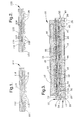
- Figures 1 and 2 represent cross-sectional views of BGA packages in accordance with the prior art.
- Figure 3 represents a cross-sectional view of a multi-chip BGA package that makes use of a pair of substrates attached together to form a chip carrier and input/output interface structure in accordance with the present invention.
- Figure 4 is a plan view of the package of Figure 3, in which a mold compound is omitted to reveal flip chips mounted within the package.
- Figure 5 is a plan view of one of the substrates of the package of Figures 3 and 4.
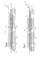
- Figures 6 and 7 represent alternative configurations for gating and venting the package of Figure 3 in accordance with the present invention.
-
- A flip-
chip package 10 in accordance with this invention is represented in cross-section in Figure 3. As shown, thepackage 10 includes a pair of laminate PCB's 12 and 14 that are secured together to form a unitary chip carrier and input/output (I/O) interface structure for a number offlip chips 16 mounted to both surfaces of one of the PCB's 12. As such, thepackage 10 can be termed a dual-sided flip-chip MCM BGA package. Whileflip chips 16 are illustrated in the Figures, various types of circuit components could be present in thepackage 10 in addition to or in place of theflip chips 16, for example, wire-bonded chips and/or other surface-mount components. - The upper PCB 12 (as viewed in Figure 3) is shown as a multilayer laminate substrate, though other types of substrates could foreseeably be used. The
flip chips 16 are mounted toopposite surfaces PCB 12, as can be other surface-mounted (SM) components, such that the PCB 12 will be referred to as thecarrier PCB 12. In accordance with flip-chip mounting techniques, thechips 16 are physically and electrically connected to conductor patterns on thechip carrier PCB 12 with solderjoint connections 22 formed by reflowing solder bumps on thechips 16. - The
second PCB 14 is depicted as a two-layer laminate substrate, though again other substrate configurations are within the scope of this invention. Onesurface 24 of thePCB 14 faces thecarrier PCB 12, while theopposite surface 26 is equipped withsolder balls 28 attached tobond pads 30, through which I/O signals from thechips 16 can be communicated with a mother board (not shown) to which thepackage 10 is eventually mounted. As such, the PCB 14 will be referred to as the I/O PCB 14. The I/O PCB 14 can be attached to thecarrier PCB 12 by a suitable method that allows electrical interconnection between the two PCB's 12 and 14. The PCB's 12 and 14 may be attached at the manufacturing level, or in a subsequent operation with a conductive adhesive or, as represented in Figure 3,solder 32. Whatever the attachment method, electrical paths must be provided between theflip chip connections 22 and thesolder balls 28, such as through metallizedvias 56 through the I/O PCB 14. - As is apparent from Figures 3, 4 and 5, the I/
O PCB 14 is fabricated to have aninterior opening 38, with the remainder of thePCB 14 defining aframe 40 that surrounds theopening 38. The opening 38 andframe 40 are illustrated as having rectangular shapes, though other shapes could be employed. As a result of the manner in which the PCB's 12 and 14 are assembled, theopening 38 in the I/O PCB 14 defines acavity 42 in which are contained theflip chips 16 attached to thelower surface 20 of thecarrier PCB 12. As also depicted in Figure 3, thecavity 42 contains acompound 44 that encapsulate theflip chips 16 attached to thelower surface 20 of thecarrier PCB 12. For this purpose, thepackage 10 is equipped with agate 46 and vent 48 through which a suitable polymeric material can be injected into thecavity 42 to form thecompound 44. Thegate 46 andvent 48 are represented in Figures 3 through 5 as being formed by removing material from thesurface 24 of the I/O PCB 14, preferably at two opposing corners of thePCB 14. In Figure 5, the I/O PCB 14 is shown as having twoslots surface 24, thewider slot 50 corresponding to thegate 46 and thenarrower slot 52 corresponding to thevent 48. Theslots O PCB 14. When the I/O PCB 14 is assembled to thecarrier PCB 12, theslots gate 46 andvent 48 are buried at opposite corners of thepackage 10. - To fill the
cavity 42 with themold compound 44, a film-assisted molding (FAME) technique is preferably utilized. As represented in Figure 6, afilm 58 is applied to thelower surface 26 of the I/O PCB 14 prior to placement of thesolder balls 28. A suitable liquid polymeric material, such as a thermoset epoxy, is then injected with anozzle 60 through thegate 46 and into thecavity 42, and is thereafter cured to form thecompound 44. As depicted in Figure 6, the same polymeric material can be simultaneously injected with thenozzle 60 onto theupper surface 18 of thecarrier PCB 12 to form amold compound 54 that, as shown in Figure 3, encapsulates and preferably underfills thechips 16 on theupper surface 18 of thePCB 12. As thecavity 42 fills with the polymeric material, the gaseous contents of thecavity 42, e.g., air, escape through thevent 48. Placement of thegate 46 and vent 48 at the package corners promotes the ability of the liquid polymeric material to completely fill thecavity 42 and reduces the occurrence of voids within thecompound 44. An alternative approach is depicted in Figure 7, in which thegate 46 is replaced with at least oneinternal gate 64, shown in the form of a through-hole in thePCB 12. In this embodiment, the polymeric material is injected with anozzle 62 onto theupper surface 18 of thecarrier PCB 12, and then flows downward into thecavity 42 through theinternal gate 64. As before, the gaseous contents of thecavity 42 escape through thevent 48 as thecavity 42 fills with the polymeric material. - From the above description, it can be appreciated that a liquid material can be injected into the
cavity 42 to both underfill and overmold thechips 16 on thelower surface 20 of thecarrier PCB 12, and can be simultaneously deposited on theupper surface 18 of thePCB 12 to encapsulate andunderfill chips 16 on theupper surface 18. The resultingpackage 10 thus has all of its chips 16 (as well as any other devices mounted to the carrier PCB 12), mechanically protected from extraneous damage as well as underfilled to promote the reliability of theirsolder connections 22. Also from the above description, it can be appreciated that the layouts of the PCB's 12 and 14 can be configured such that thepackage 10 can be molded in strip form, in whichmultiple packages 10 can be simultaneously molded in a single operation. In so doing, the manufacturing efficiency of thepackage 10 is increased while decreasing costs. The result is a cost-effective, high-density packaging technique by which various electrical components (flip chips 16, etc.) are mechanically protected within an electrically-testable package 10. These advantages are achieved while eliminating a separate underfill process, preferably utilizing instead a single molding operation during which chips 16 on bothsurfaces carrier PCB 12 are simultaneously underfilled and overmolded. - While the invention has been described in terms of a preferred embodiment, it is apparent that other forms could be adopted by one skilled in the art. Accordingly, the scope of the invention is to be limited only by the following claims.
Claims (20)
- A package (10) comprising:a first laminate substrate (12) having a first conductor pattern on a first surface (18) thereof and a second conductor pattern on an oppositely-disposed second surface (20) thereof;a second laminate substrate (14) attached to the first laminate substrate (12), the second laminate substrate (14) having an interior opening (38) therethrough and a frame portion (40) surrounding the interior opening (38), the frame portion (40) having a first surface (24) facing the first laminate substrate (12) and an oppositely-disposed second surface (26) on which solder terminals (28) are present;at least a first surface-mounted device (16) on the first surface (18) of the first laminate substrate (12) and electrically connected to the first conductor pattern; andat least a second surface-mounted device (16) on the second surface (20) of the first laminate substrate (12) and electrically connected to the second conductor pattern, the first and second laminate substrates (12,14) being attached so that the second surface-mounted device (16) is disposed within the interior opening (38) of the second laminate substrate (14).
- A package (10) according to claim 1, wherein at least one of the first and second surface-mounted devices (16) is a flip chip having solder bump terminals (22) on a surface thereof that physically and electrically connect the flip chip to the first laminate substrate (12).
- A package (10) according to claim 1, wherein the first and second surface-mounted devices (16) are flip chips having solder bump terminals (22) on respective surfaces thereof, the solder bump terminals (22) of the first surface-mounted device (16) physically and electrically connecting the first surface-mounted device (16) to the first conductor pattern on the first surface (18) of the first laminate substrate (12), the solder bump terminals (22) of the second surface-mounted device (16) physically and electrically connecting the second surface-mounted device (16) to the second conductor pattern on the second surface (20) of the first laminate substrate (12).
- A package (10) according to claim 1, wherein the second laminate substrate (14) is electrically connected to the first laminate substrate (12), and the second laminate substrate (14) has conductors (56) that electrically connect the first and second conductor patterns on the first laminate substrate (12) to the solder terminals (28) on the second surface (26) of the second laminate substrate (14).
- A package (10) according to claim 1, wherein the second laminate substrate (14) has first and second lateral openings (46,48) interconnecting the interior opening (38) with an outer perimeter of the second laminate substrate (14).
- A package (10) according to claim 5, wherein the second laminate substrate (14) and the interior opening (38) have rectangular shapes, the first lateral opening (46) is located at a first corner of the second laminate substrate (14), and the second lateral opening (48) is located at a diagonally-opposed second corner of the second laminate substrate (14).
- A package (10) according to claim 5, wherein the first and second lateral opening (46,48) are defined in the first surface (24) of the second laminate substrate (14) so as to be between the first and second laminate substrates (12,14).
- A package (10) according to claim 1, further comprising a molding compound (44) that fills the interior opening (38) of the second laminate substrate (14) and both underfills and encapsulates the second surface-mounted device (16).
- A package (10) according to claim 8, further comprising a molding compound (54) on the first surface (18) of the first laminate substrate (12) that encapsulates the first surface-mounted device (16).
- A package (10) according to claim 9, wherein the first laminate substrate (12) has at least one opening (64) therethrough that interconnects the molding compound (54) on the first surface (18) of the first laminate substrate (12) with the molding compound (44) within the interior opening (38) of the second laminate substrate (14).
- A method of forming a package (10), the method comprising the steps of:providing a first laminate substrate (12) having a first conductor pattern on a first surface (18) thereof and a second conductor pattern on an oppositely-disposed second surface (20) thereof;attaching a second laminate substrate (14) to the first laminate substrate (12), the second laminate substrate (14) having an interior opening (38) therethrough and a frame portion (40) surrounding the interior opening (38), the frame portion (40) having a first surface (24) facing the first laminate substrate (12) and an oppositely-disposed second surface (26) on which solder terminals (28) are present;mounting at least a first surface-mounted device (16) to the first surface (18) of the first laminate substrate (12) so that the first surface-mounted device (16) is electrically connected to the first conductor pattern; andmounting at least a second surface-mounted device (16) to the second surface (20) of the first laminate substrate (12) so that the second surface-mounted device (16) is electrically connected to the second conductor pattern, the first and second laminate substrates (12,14) being attached so that the second surface-mounted device (16) is disposed within the interior opening (38) of the second laminate substrate (14).
- A method according to claim 11, wherein at least one of the first and second surface-mounted devices (16) is flip-chip mounted with solder bump terminals (22) on a surface thereof.
- A method according to claim 11, wherein the first and second surface-mounted devices (16) are flip chips having solder bump terminals (22) on respective surfaces thereof, the first and second surface-mounted devices (16) are flip-chip mounted with the solder bump terminals (22) thereof to the first conductor pattern on the first surface (18) of the first laminate substrate (12), and the second surface-mounted devices (16) are flip-chip mounted with the solder bump terminals (22) thereof to the second conductor pattern on the second surface (20) of the first laminate substrate (12).
- A method according to claim 11, further comprising the step of forming the second laminate substrate (14) with conductors (56) that, when the second laminate substrate (14) is attached to the first laminate substrate (12), electrically connect the first and second conductor patterns on the first laminate substrate (12) to the solder terminals (28) on the second surface (26) of the second laminate substrate (14).
- A method according to claim 11, further comprising the step of forming the second laminate substrate (14) to have first and second lateral openings (46,48) interconnecting the interior opening (38) with an outer perimeter of the second laminate substrate (14).
- A method according to claim 15, further comprising the step of forming the second laminate substrate (14) and the interior opening (38) thereof to have rectangular shapes, the first lateral opening (46) being located at a first corner of the second laminate substrate (14), and the second lateral opening (48) being located at a diagonally-opposite second corner of the second laminate substrate (14).
- A method according to claim 16, wherein the first and second lateral openings (46,48) are formed in the first surface (24) of the second laminate substrate (14) so as to be between the first and second laminate substrates (12,14) after the attaching step.
- A method according to claim 17, further comprising the step of injecting a molding compound (44) through one of the lateral openings (46) into the interior opening (38) of the second laminate substrate (14) to both underfill and encapsulate the second surface-mounted device (16).
- A method according to claim 11, further comprising the step of applying a molding compound (54) that encapsulates the first surface-mounted device (16).
- A method according to claim 11, further comprising the steps of:forming the first laminate substrate (12) to have at least one opening (64) therethrough; andinjecting a molding compound (44,54) that encapsulates the first surface-mounted device (16) and flows through the opening (64) into the interior opening (38) of the second laminate substrate (14) to both underfill and encapsulate the second surface-mounted device (16).
Applications Claiming Priority (2)
| Application Number | Priority Date | Filing Date | Title |
|---|---|---|---|
| US10/321,900 US6833628B2 (en) | 2002-12-17 | 2002-12-17 | Mutli-chip module |
| US321900 | 2002-12-17 |
Publications (2)
| Publication Number | Publication Date |
|---|---|
| EP1432033A1 true EP1432033A1 (en) | 2004-06-23 |
| EP1432033B1 EP1432033B1 (en) | 2006-11-02 |
Family
ID=32393007
Family Applications (1)
| Application Number | Title | Priority Date | Filing Date |
|---|---|---|---|
| EP03078782A Expired - Lifetime EP1432033B1 (en) | 2002-12-17 | 2003-11-28 | Multi-chip module and method of forming |
Country Status (3)
| Country | Link |
|---|---|
| US (2) | US6833628B2 (en) |
| EP (1) | EP1432033B1 (en) |
| DE (1) | DE60309422T2 (en) |
Cited By (1)
| Publication number | Priority date | Publication date | Assignee | Title |
|---|---|---|---|---|
| WO2009124246A1 (en) * | 2008-04-04 | 2009-10-08 | The Charles Stark Draper Laboratory, Inc. | Interposers, electronic modules, and methods for forming the same |
Families Citing this family (40)
| Publication number | Priority date | Publication date | Assignee | Title |
|---|---|---|---|---|
| TW569416B (en) * | 2002-12-19 | 2004-01-01 | Via Tech Inc | High density multi-chip module structure and manufacturing method thereof |
| US6916684B2 (en) * | 2003-03-18 | 2005-07-12 | Delphi Technologies, Inc. | Wafer-applied underfill process |
| DE10323007B4 (en) * | 2003-05-21 | 2005-10-20 | Infineon Technologies Ag | A semiconductor device |
| US20050017337A1 (en) * | 2003-07-21 | 2005-01-27 | Cherng-Chiao Wu | Stacking apparatus for integrated circuit assembly |
| KR101075169B1 (en) * | 2003-08-27 | 2011-10-19 | 페어차일드코리아반도체 주식회사 | Power module flip chip package |
| JP2005158814A (en) * | 2003-11-20 | 2005-06-16 | Alps Electric Co Ltd | Electronic circuit unit |
| WO2005067029A1 (en) * | 2004-01-06 | 2005-07-21 | Infineon Technologies Ag | Method for packaging integrated circuit dies |
| KR100640335B1 (en) * | 2004-10-28 | 2006-10-30 | 삼성전자주식회사 | Land grid array module |
| US7473585B2 (en) * | 2005-06-13 | 2009-01-06 | Delphi Technologies, Inc. | Technique for manufacturing an overmolded electronic assembly |
| US20070158811A1 (en) * | 2006-01-11 | 2007-07-12 | James Douglas Wehrly | Low profile managed memory component |
| KR100782774B1 (en) * | 2006-05-25 | 2007-12-05 | 삼성전기주식회사 | SPI module |
| TW200807647A (en) * | 2006-07-17 | 2008-02-01 | Delta Electronics Inc | Integrated circuit module |
| JP4927162B2 (en) * | 2007-03-29 | 2012-05-09 | 京セラ株式会社 | Portable radio |
| US8134227B2 (en) * | 2007-03-30 | 2012-03-13 | Stats Chippac Ltd. | Stacked integrated circuit package system with conductive spacer |
| US7915089B2 (en) * | 2007-04-10 | 2011-03-29 | Infineon Technologies Ag | Encapsulation method |
| US8139371B2 (en) * | 2007-07-30 | 2012-03-20 | GM Global Technology Operations LLC | Power electronics devices with integrated control circuitry |
| US7973433B2 (en) * | 2007-07-30 | 2011-07-05 | Nelson David F | Power electronics devices with integrated gate drive circuitry |
| US8017451B2 (en) | 2008-04-04 | 2011-09-13 | The Charles Stark Draper Laboratory, Inc. | Electronic modules and methods for forming the same |
| US9293350B2 (en) * | 2008-10-28 | 2016-03-22 | Stats Chippac Ltd. | Semiconductor package system with cavity substrate and manufacturing method therefor |
| US8618654B2 (en) * | 2010-07-20 | 2013-12-31 | Marvell World Trade Ltd. | Structures embedded within core material and methods of manufacturing thereof |
| KR101088824B1 (en) * | 2010-06-16 | 2011-12-06 | 주식회사 하이닉스반도체 | Module substrate, memory module having same and method for forming memory module |
| CN106935577A (en) * | 2011-03-22 | 2017-07-07 | 晶元光电股份有限公司 | LED device |
| US8514576B1 (en) * | 2011-06-14 | 2013-08-20 | Juniper Networks, Inc. | Dual sided system in a package |
| EP2565913B1 (en) * | 2011-06-22 | 2019-03-20 | Huawei Device Co., Ltd. | Method for encapsulating of a semiconductor |
| US20130020702A1 (en) * | 2011-07-21 | 2013-01-24 | Jun Zhai | Double-sided flip chip package |
| US20130082383A1 (en) * | 2011-10-03 | 2013-04-04 | Texas Instruments Incorporated | Electronic assembly having mixed interface including tsv die |
| US8698323B2 (en) * | 2012-06-18 | 2014-04-15 | Invensas Corporation | Microelectronic assembly tolerant to misplacement of microelectronic elements therein |
| KR20150025129A (en) * | 2013-08-28 | 2015-03-10 | 삼성전기주식회사 | Electric component module and manufacturing method threrof |
| US9076802B1 (en) * | 2013-09-25 | 2015-07-07 | Stats Chippac Ltd. | Dual-sided film-assist molding process |
| CN104576411A (en) * | 2013-10-25 | 2015-04-29 | 飞思卡尔半导体公司 | Top gateway mold with double corners |
| US9392695B2 (en) * | 2014-01-03 | 2016-07-12 | Samsung Electro-Mechanics Co., Ltd. | Electric component module |
| US9666559B2 (en) * | 2014-09-05 | 2017-05-30 | Invensas Corporation | Multichip modules and methods of fabrication |
| TWI590392B (en) * | 2015-08-03 | 2017-07-01 | 矽品精密工業股份有限公司 | Electronic package and its manufacturing method |
| TWI676259B (en) * | 2016-09-02 | 2019-11-01 | 矽品精密工業股份有限公司 | Electronic package and method for fabricating the same |
| KR20180090527A (en) * | 2017-02-03 | 2018-08-13 | 삼성전기주식회사 | Semiconductor package and manufacturing method threrof |
| EP3869924A1 (en) * | 2020-02-21 | 2021-08-25 | Harman Becker Automotive Systems GmbH | Double-side pcb sip assembly |
| US12087733B2 (en) | 2021-05-13 | 2024-09-10 | Taiwan Semiconductor Manufacturing Co., Ltd. | Packages with multiple types of underfill and method forming the same |
| US11747555B2 (en) | 2021-10-04 | 2023-09-05 | Eagle Technology, Llc | Optical assembly having commonly-shaped optical modules and associated methods |
| US12394721B2 (en) * | 2022-12-20 | 2025-08-19 | Nanya Technology Corporation | Package structure including at least two electronic components |
| KR20240116223A (en) * | 2023-01-20 | 2024-07-29 | 삼성전자주식회사 | Semiconductor package |
Citations (7)
| Publication number | Priority date | Publication date | Assignee | Title |
|---|---|---|---|---|
| US5448825A (en) * | 1993-03-25 | 1995-09-12 | Vlsi Technology, Inc. | Method of making electrically and thermally enhanced integrated-circuit package |
| US5570274A (en) * | 1993-11-29 | 1996-10-29 | Nec Corporation | High density multichip module packaging structure |
| US5615089A (en) * | 1994-07-26 | 1997-03-25 | Fujitsu Limited | BGA semiconductor device including a plurality of semiconductor chips located on upper and lower surfaces of a first substrate |
| US5981312A (en) * | 1997-06-27 | 1999-11-09 | International Business Machines Corporation | Method for injection molded flip chip encapsulation |
| EP1096567A2 (en) * | 1999-10-25 | 2001-05-02 | Oki Electric Industry Co., Ltd. | BGA package and method for fabricating the same |
| US20010013640A1 (en) * | 1997-10-24 | 2001-08-16 | Tetsuya Tao | Semiconductor device package having separate substrate, strengthening ring and cap structures |
| US6285559B1 (en) * | 1998-05-26 | 2001-09-04 | Nec Corporation | Multichip module |
Family Cites Families (6)
| Publication number | Priority date | Publication date | Assignee | Title |
|---|---|---|---|---|
| US5914A (en) * | 1848-11-14 | Odometer | ||
| US13640A (en) * | 1855-10-09 | Corlil-sheitleb | ||
| US5608262A (en) * | 1995-02-24 | 1997-03-04 | Lucent Technologies Inc. | Packaging multi-chip modules without wire-bond interconnection |
| US5770477A (en) | 1997-02-10 | 1998-06-23 | Delco Electronics Corporation | Flip chip-on-flip chip multi-chip module |
| JP3359846B2 (en) * | 1997-07-18 | 2002-12-24 | シャープ株式会社 | Semiconductor device |
| US6383846B1 (en) * | 2000-03-20 | 2002-05-07 | Chi-Chih Shen | Method and apparatus for molding a flip chip semiconductor device |
-
2002
- 2002-12-17 US US10/321,900 patent/US6833628B2/en not_active Expired - Fee Related
-
2003
- 2003-11-28 EP EP03078782A patent/EP1432033B1/en not_active Expired - Lifetime
- 2003-11-28 DE DE60309422T patent/DE60309422T2/en not_active Expired - Fee Related
-
2004
- 2004-12-15 US US11/012,401 patent/US20050093144A1/en not_active Abandoned
Patent Citations (7)
| Publication number | Priority date | Publication date | Assignee | Title |
|---|---|---|---|---|
| US5448825A (en) * | 1993-03-25 | 1995-09-12 | Vlsi Technology, Inc. | Method of making electrically and thermally enhanced integrated-circuit package |
| US5570274A (en) * | 1993-11-29 | 1996-10-29 | Nec Corporation | High density multichip module packaging structure |
| US5615089A (en) * | 1994-07-26 | 1997-03-25 | Fujitsu Limited | BGA semiconductor device including a plurality of semiconductor chips located on upper and lower surfaces of a first substrate |
| US5981312A (en) * | 1997-06-27 | 1999-11-09 | International Business Machines Corporation | Method for injection molded flip chip encapsulation |
| US20010013640A1 (en) * | 1997-10-24 | 2001-08-16 | Tetsuya Tao | Semiconductor device package having separate substrate, strengthening ring and cap structures |
| US6285559B1 (en) * | 1998-05-26 | 2001-09-04 | Nec Corporation | Multichip module |
| EP1096567A2 (en) * | 1999-10-25 | 2001-05-02 | Oki Electric Industry Co., Ltd. | BGA package and method for fabricating the same |
Cited By (1)
| Publication number | Priority date | Publication date | Assignee | Title |
|---|---|---|---|---|
| WO2009124246A1 (en) * | 2008-04-04 | 2009-10-08 | The Charles Stark Draper Laboratory, Inc. | Interposers, electronic modules, and methods for forming the same |
Also Published As
| Publication number | Publication date |
|---|---|
| US6833628B2 (en) | 2004-12-21 |
| US20050093144A1 (en) | 2005-05-05 |
| US20040113281A1 (en) | 2004-06-17 |
| DE60309422T2 (en) | 2007-10-11 |
| EP1432033B1 (en) | 2006-11-02 |
| DE60309422D1 (en) | 2006-12-14 |
Similar Documents
| Publication | Publication Date | Title |
|---|---|---|
| US6833628B2 (en) | Mutli-chip module | |
| US7791205B2 (en) | Interposers for semiconductor die packages with standard ball grill array footprint | |
| US7994626B2 (en) | Multi-layer semiconductor package with vertical connectors and method of manufacture thereof | |
| US6518089B2 (en) | Flip chip semiconductor device in a molded chip scale package (CSP) and method of assembly | |
| US6274930B1 (en) | Multi-chip module with stacked dice | |
| US6492726B1 (en) | Chip scale packaging with multi-layer flip chip arrangement and ball grid array interconnection | |
| KR100493063B1 (en) | BGA package with stacked semiconductor chips and manufacturing method thereof | |
| US8704349B2 (en) | Integrated circuit package system with exposed interconnects | |
| US6201302B1 (en) | Semiconductor package having multi-dies | |
| US7579690B2 (en) | Semiconductor package structure | |
| US5541450A (en) | Low-profile ball-grid array semiconductor package | |
| US20050263906A1 (en) | Electronic system including a semiconductor device with at least one semiconductor die, a carrier, and an encapsulant that fills a space between the die and the carrier and covers intermediate conductive elements that connect the die and the carrier | |
| KR19990047010A (en) | Semiconductor Package Substrate, Land Grid Array Semiconductor Package Using the Substrate and Method of Manufacturing The Same | |
| US6448110B1 (en) | Method for fabricating a dual-chip package and package formed | |
| US6992380B2 (en) | Package for semiconductor device having a device-supporting polymeric material covering a solder ball array area | |
| JP4339032B2 (en) | Semiconductor device | |
| KR101472901B1 (en) | Wafer level chip scale package comprising a rewiring substrate and method for manufacturing the same | |
| WO2003050851A2 (en) | A semiconductor device | |
| KR20030012503A (en) | Packaging process for semiconductor package |
Legal Events
| Date | Code | Title | Description |
|---|---|---|---|
| PUAI | Public reference made under article 153(3) epc to a published international application that has entered the european phase |
Free format text: ORIGINAL CODE: 0009012 |
|
| AK | Designated contracting states |
Kind code of ref document: A1 Designated state(s): AT BE BG CH CY CZ DE DK EE ES FI FR GB GR HU IE IT LI LU MC NL PT RO SE SI SK TR |
|
| AX | Request for extension of the european patent |
Extension state: AL LT LV MK |
|
| 17P | Request for examination filed |
Effective date: 20041223 |
|
| AKX | Designation fees paid |
Designated state(s): DE FR GB |
|
| 17Q | First examination report despatched |
Effective date: 20050203 |
|
| GRAP | Despatch of communication of intention to grant a patent |
Free format text: ORIGINAL CODE: EPIDOSNIGR1 |
|
| GRAS | Grant fee paid |
Free format text: ORIGINAL CODE: EPIDOSNIGR3 |
|
| GRAA | (expected) grant |
Free format text: ORIGINAL CODE: 0009210 |
|
| AK | Designated contracting states |
Kind code of ref document: B1 Designated state(s): DE FR GB |
|
| REG | Reference to a national code |
Ref country code: GB Ref legal event code: FG4D |
|
| REF | Corresponds to: |
Ref document number: 60309422 Country of ref document: DE Date of ref document: 20061214 Kind code of ref document: P |
|
| ET | Fr: translation filed | ||
| PLBE | No opposition filed within time limit |
Free format text: ORIGINAL CODE: 0009261 |
|
| STAA | Information on the status of an ep patent application or granted ep patent |
Free format text: STATUS: NO OPPOSITION FILED WITHIN TIME LIMIT |
|
| 26N | No opposition filed |
Effective date: 20070803 |
|
| GBPC | Gb: european patent ceased through non-payment of renewal fee |
Effective date: 20071128 |
|
| PG25 | Lapsed in a contracting state [announced via postgrant information from national office to epo] |
Ref country code: GB Free format text: LAPSE BECAUSE OF NON-PAYMENT OF DUE FEES Effective date: 20071128 |
|
| PGFP | Annual fee paid to national office [announced via postgrant information from national office to epo] |
Ref country code: DE Payment date: 20081120 Year of fee payment: 6 |
|
| PGFP | Annual fee paid to national office [announced via postgrant information from national office to epo] |
Ref country code: FR Payment date: 20091123 Year of fee payment: 7 |
|
| PG25 | Lapsed in a contracting state [announced via postgrant information from national office to epo] |
Ref country code: DE Free format text: LAPSE BECAUSE OF NON-PAYMENT OF DUE FEES Effective date: 20100601 |
|
| REG | Reference to a national code |
Ref country code: FR Ref legal event code: ST Effective date: 20110801 |
|
| PG25 | Lapsed in a contracting state [announced via postgrant information from national office to epo] |
Ref country code: FR Free format text: LAPSE BECAUSE OF NON-PAYMENT OF DUE FEES Effective date: 20101130 |