EP1432027A1 - HIGH FREQUENCY IC PACKAGE, HIGH FREQUENCY UNIT USING IT, AND METHOD FOR MANUFACTURING THE SAME - Google Patents
HIGH FREQUENCY IC PACKAGE, HIGH FREQUENCY UNIT USING IT, AND METHOD FOR MANUFACTURING THE SAME Download PDFInfo
- Publication number
- EP1432027A1 EP1432027A1 EP01982852A EP01982852A EP1432027A1 EP 1432027 A1 EP1432027 A1 EP 1432027A1 EP 01982852 A EP01982852 A EP 01982852A EP 01982852 A EP01982852 A EP 01982852A EP 1432027 A1 EP1432027 A1 EP 1432027A1
- Authority
- EP
- European Patent Office
- Prior art keywords
- high frequency
- package
- board
- circuit board
- chip
- Prior art date
- Legal status (The legal status is an assumption and is not a legal conclusion. Google has not performed a legal analysis and makes no representation as to the accuracy of the status listed.)
- Withdrawn
Links
Images




Classifications
-
- H—ELECTRICITY
- H05—ELECTRIC TECHNIQUES NOT OTHERWISE PROVIDED FOR
- H05K—PRINTED CIRCUITS; CASINGS OR CONSTRUCTIONAL DETAILS OF ELECTRIC APPARATUS; MANUFACTURE OF ASSEMBLAGES OF ELECTRICAL COMPONENTS
- H05K1/00—Printed circuits
- H05K1/02—Details
- H05K1/0213—Electrical arrangements not otherwise provided for
- H05K1/0216—Reduction of cross-talk, noise or electromagnetic interference
- H05K1/023—Reduction of cross-talk, noise or electromagnetic interference using auxiliary mounted passive components or auxiliary substances
- H05K1/0231—Capacitors or dielectric substances
-
- H—ELECTRICITY
- H10—SEMICONDUCTOR DEVICES; ELECTRIC SOLID-STATE DEVICES NOT OTHERWISE PROVIDED FOR
- H10W—GENERIC PACKAGES, INTERCONNECTIONS, CONNECTORS OR OTHER CONSTRUCTIONAL DETAILS OF DEVICES COVERED BY CLASS H10
- H10W76/00—Containers; Fillings or auxiliary members therefor; Seals
- H10W76/10—Containers or parts thereof
-
- H—ELECTRICITY
- H10—SEMICONDUCTOR DEVICES; ELECTRIC SOLID-STATE DEVICES NOT OTHERWISE PROVIDED FOR
- H10W—GENERIC PACKAGES, INTERCONNECTIONS, CONNECTORS OR OTHER CONSTRUCTIONAL DETAILS OF DEVICES COVERED BY CLASS H10
- H10W44/00—Electrical arrangements for controlling or matching impedance
- H10W44/20—Electrical arrangements for controlling or matching impedance at high-frequency [HF] or radio frequency [RF]
-
- H—ELECTRICITY
- H10—SEMICONDUCTOR DEVICES; ELECTRIC SOLID-STATE DEVICES NOT OTHERWISE PROVIDED FOR
- H10W—GENERIC PACKAGES, INTERCONNECTIONS, CONNECTORS OR OTHER CONSTRUCTIONAL DETAILS OF DEVICES COVERED BY CLASS H10
- H10W44/00—Electrical arrangements for controlling or matching impedance
- H10W44/601—Capacitive arrangements
-
- H—ELECTRICITY
- H05—ELECTRIC TECHNIQUES NOT OTHERWISE PROVIDED FOR
- H05K—PRINTED CIRCUITS; CASINGS OR CONSTRUCTIONAL DETAILS OF ELECTRIC APPARATUS; MANUFACTURE OF ASSEMBLAGES OF ELECTRICAL COMPONENTS
- H05K1/00—Printed circuits
- H05K1/02—Details
- H05K1/0213—Electrical arrangements not otherwise provided for
- H05K1/0237—High frequency adaptations
- H05K1/0243—Printed circuits associated with mounted high frequency components
-
- H—ELECTRICITY
- H05—ELECTRIC TECHNIQUES NOT OTHERWISE PROVIDED FOR
- H05K—PRINTED CIRCUITS; CASINGS OR CONSTRUCTIONAL DETAILS OF ELECTRIC APPARATUS; MANUFACTURE OF ASSEMBLAGES OF ELECTRICAL COMPONENTS
- H05K2201/00—Indexing scheme relating to printed circuits covered by H05K1/00
- H05K2201/10—Details of components or other objects attached to or integrated in a printed circuit board
- H05K2201/10431—Details of mounted components
- H05K2201/10507—Involving several components
- H05K2201/10545—Related components mounted on both sides of the PCB
-
- H—ELECTRICITY
- H05—ELECTRIC TECHNIQUES NOT OTHERWISE PROVIDED FOR
- H05K—PRINTED CIRCUITS; CASINGS OR CONSTRUCTIONAL DETAILS OF ELECTRIC APPARATUS; MANUFACTURE OF ASSEMBLAGES OF ELECTRICAL COMPONENTS
- H05K2201/00—Indexing scheme relating to printed circuits covered by H05K1/00
- H05K2201/10—Details of components or other objects attached to or integrated in a printed circuit board
- H05K2201/10613—Details of electrical connections of non-printed components, e.g. special leads
- H05K2201/10621—Components characterised by their electrical contacts
- H05K2201/10689—Leaded Integrated Circuit [IC] package, e.g. dual-in-line [DIL]
-
- H—ELECTRICITY
- H05—ELECTRIC TECHNIQUES NOT OTHERWISE PROVIDED FOR
- H05K—PRINTED CIRCUITS; CASINGS OR CONSTRUCTIONAL DETAILS OF ELECTRIC APPARATUS; MANUFACTURE OF ASSEMBLAGES OF ELECTRICAL COMPONENTS
- H05K2203/00—Indexing scheme relating to apparatus or processes for manufacturing printed circuits covered by H05K3/00
- H05K2203/11—Treatments characterised by their effect, e.g. heating, cooling, roughening
- H05K2203/1147—Sealing or impregnating, e.g. of pores
-
- H—ELECTRICITY
- H10—SEMICONDUCTOR DEVICES; ELECTRIC SOLID-STATE DEVICES NOT OTHERWISE PROVIDED FOR
- H10W—GENERIC PACKAGES, INTERCONNECTIONS, CONNECTORS OR OTHER CONSTRUCTIONAL DETAILS OF DEVICES COVERED BY CLASS H10
- H10W72/00—Interconnections or connectors in packages
- H10W72/071—Connecting or disconnecting
- H10W72/075—Connecting or disconnecting of bond wires
-
- H—ELECTRICITY
- H10—SEMICONDUCTOR DEVICES; ELECTRIC SOLID-STATE DEVICES NOT OTHERWISE PROVIDED FOR
- H10W—GENERIC PACKAGES, INTERCONNECTIONS, CONNECTORS OR OTHER CONSTRUCTIONAL DETAILS OF DEVICES COVERED BY CLASS H10
- H10W72/00—Interconnections or connectors in packages
- H10W72/50—Bond wires
- H10W72/531—Shapes of wire connectors
- H10W72/536—Shapes of wire connectors the connected ends being ball-shaped
-
- H—ELECTRICITY
- H10—SEMICONDUCTOR DEVICES; ELECTRIC SOLID-STATE DEVICES NOT OTHERWISE PROVIDED FOR
- H10W—GENERIC PACKAGES, INTERCONNECTIONS, CONNECTORS OR OTHER CONSTRUCTIONAL DETAILS OF DEVICES COVERED BY CLASS H10
- H10W72/00—Interconnections or connectors in packages
- H10W72/50—Bond wires
- H10W72/531—Shapes of wire connectors
- H10W72/5363—Shapes of wire connectors the connected ends being wedge-shaped
-
- H—ELECTRICITY
- H10—SEMICONDUCTOR DEVICES; ELECTRIC SOLID-STATE DEVICES NOT OTHERWISE PROVIDED FOR
- H10W—GENERIC PACKAGES, INTERCONNECTIONS, CONNECTORS OR OTHER CONSTRUCTIONAL DETAILS OF DEVICES COVERED BY CLASS H10
- H10W72/00—Interconnections or connectors in packages
- H10W72/50—Bond wires
- H10W72/551—Materials of bond wires
-
- H—ELECTRICITY
- H10—SEMICONDUCTOR DEVICES; ELECTRIC SOLID-STATE DEVICES NOT OTHERWISE PROVIDED FOR
- H10W—GENERIC PACKAGES, INTERCONNECTIONS, CONNECTORS OR OTHER CONSTRUCTIONAL DETAILS OF DEVICES COVERED BY CLASS H10
- H10W72/00—Interconnections or connectors in packages
- H10W72/851—Dispositions of multiple connectors or interconnections
- H10W72/874—On different surfaces
- H10W72/884—Die-attach connectors and bond wires
-
- H—ELECTRICITY
- H10—SEMICONDUCTOR DEVICES; ELECTRIC SOLID-STATE DEVICES NOT OTHERWISE PROVIDED FOR
- H10W—GENERIC PACKAGES, INTERCONNECTIONS, CONNECTORS OR OTHER CONSTRUCTIONAL DETAILS OF DEVICES COVERED BY CLASS H10
- H10W72/00—Interconnections or connectors in packages
- H10W72/90—Bond pads, in general
- H10W72/951—Materials of bond pads
-
- H—ELECTRICITY
- H10—SEMICONDUCTOR DEVICES; ELECTRIC SOLID-STATE DEVICES NOT OTHERWISE PROVIDED FOR
- H10W—GENERIC PACKAGES, INTERCONNECTIONS, CONNECTORS OR OTHER CONSTRUCTIONAL DETAILS OF DEVICES COVERED BY CLASS H10
- H10W90/00—Package configurations
- H10W90/701—Package configurations characterised by the relative positions of pads or connectors relative to package parts
- H10W90/731—Package configurations characterised by the relative positions of pads or connectors relative to package parts of die-attach connectors
- H10W90/737—Package configurations characterised by the relative positions of pads or connectors relative to package parts of die-attach connectors between a chip and a laterally-adjacent lead frame, conducting package substrate or heat sink
Definitions
- the present invention relates to a high frequency IC package, a high frequency unit using the high frequency IC package, and a method of manufacturing the high frequency unit.
- a millimeter wave or micro-wave unit (high frequency unit) used for a radar system incorporated into a vehicle is composed in such a manner that a circuit board, on which various parts are mounted, and MMIC package (Monolithic Microwave Integrated Circuit) (high frequency IC package) are mounted on a housing chassis.
- MMIC package Monitoring Microwave Integrated Circuit
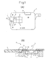
- Fig. 1 is a view showing a structure of a conventional high frequency unit.
- Fig. 1 (A) is a plan view showing an outline of the arrangement, and
- Fig. 1(B) is a sectional view taken on line B - B in Fig. 1(A).
- the circuit board 4 and six high frequency IC packages (MMIC packages) 5 are mounted on the housing chassis 1 via the conductive adhesive 2, 3 which will be referred to as an "adhesive" hereinafter.
- Other parts such as a connector 25 are mounted on the circuit board 4 and, further, the wave guide 26 is formed in the housing chassis 1.
- the high frequency unit 6 is composed.
- solder or gold or tin brazing may be used as the adhesive.
- Fig. 2(A) is a sectional side view
- Fig. 2(B) is a bottom view of the high frequency IC package 5 from which the cap 14 has been removed.
- wiring patterns 11 connected to the high frequency IC chip 8.
- wiring patterns 12 connected to an external circuit.
- the wiring patterns 11 on the lower face are connected to the wiring patterns 12 on the upper face via the via hole 13.
- the high frequency IC chip 8 is mounted on the lower face wiring pattern 11 on the board 7.
- the bypass condensers 9 are mounted on the wiring pattern 11.
- the bypass condensers 9 are parts for determining a characteristic of the high frequency IC.
- the bypass condensers 9 are provided for preventing the oscillation of the high frequency IC.
- a ground pattern 10 On the lower face of the board 7, there is provided a ground pattern 10.
- One of the electrodes of the bypass condenser 9 is connected to the ground pattern 10 by means of wire bonding connection 15.
- the high frequency IC chip 8 and bypass condensers 9 are sealed by the cap 14.
- the bypass condensers 9 are contained in the cap 14 together with the high frequency IC chip 8. Therefore, it is necessary to conduct MCM mounting (Multi-chip module mounting), which causes difficult technical problems. Further, the package size is increased and the number of the manufacturing processes is increased. Therefore, it is difficult to reduce the manufacturing cost. As a result, it is difficult to reduce the size and cost of a millimeter wave unit in which the above high frequency IC package is used.
- the present invention has been achieved to accomplish the above objects.
- parts for compensating a characteristic
- parts for determining the characteristic of the high frequency IC chip are mounted on the board outside the seal of the high frequency IC package.
- the above parts are a bypass condenser, a coupling condenser, a temperature compensating condenser, a temperature compensating resistance and an impedance adjusting inductance.
- the above parts may be attached to either one surface of the board, on which the high frequency IC package is mounted, the high frequency IC chip being mounted on the surface, or the other surface of the board.
- the parts conventionally mounted inside the sealing are mounted outside the sealing. Therefore, the high frequency IC package can be downsized and, further, it becomes unnecessary to conduct MCM mounting. Accordingly, the occurrence of defective chip connection can be decreased, and the yield can be enhanced.
- a high frequency unit including a high frequency IC package, a circuit board, on which the peripheral circuit is mounted, and a housing chassis on which the high frequency IC package and the circuit board are mounted, parts to determine a characteristic of the high frequency IC package are mounted on a circuit board onto which the peripheral circuit is incorporated.
- a high frequency unit including a high frequency IC package, a circuit board, on which the peripheral circuit is mounted, and a housing chassis on which the high frequency IC package and the circuit board are mounted, parts to determine a characteristic of the high frequency IC package are mounted on a housing chassis.
- parts to determine a characteristic of the high frequency IC package can be automatically mounted by a mounting device. Due to the foregoing, it possible to reduce the number of manufacturing processes compared with above first aspect. Therefore, the manufacturing cost can be reduced.
- a bypass condenser is used as a part for determining a characteristic of a high frequency IC chip.
- a coupling condenser, a temperature compensating condenser, a temperature compensating resistor and an impedance adjusting inductance can be used as a part for determining a characteristic of a high frequency IC chip.
- Fig. 3(A) is a plan view showing an outline of the structure of a high frequency unit.
- Fig. 3(B) is a sectional view taken on line B - B in Fig. 3(A). This sectional view shows the structure in detail.
- Fig. 4 is an upper view of the high frequency IC package.
- the high frequency unit 6 is composed in such a manner that the circuit board 4 and two pieces of high frequency IC packages 5 are mounted on the housing chassis 1 via the conductive adhesive 2, 3 which will be referred to as an "adhesive" hereinafter. Further, the connector 25 and other parts are mounted on the circuit board 4, and the wave guide 26 is formed in the housing chassis 1. Furthermore, in the region 38 on the circuit board 4 indicated by two-dotted chain lines in Fig. 3, there are provided surface mounting parts such as an electric power source circuit on the input side of the high frequency IC package 5 and an amplifying circuit on the output side which compose an input and output circuit (peripheral circuit) with respect to the high frequency IC package 5.
- wiring patterns 11 On the lower face of the board 7 of the high frequency IC package 5, there are provided wiring patterns 11 for mounting the high frequency IC chip 8. On the upper face of the board 7 of the high frequency IC package 5, there are provided wiring patterns 12, which are connected with external circuits and ground patterns 19.
- the wiring patterns 11 and 12 are connected with each other via the via holes 13.
- the high frequency IC chip 8 is mounted on the wiring patterns 11 provided on the lower face of the board 7. Therefore, the high frequency IC chip 8 is connected with the wiring patterns 11.
- the high frequency IC chip 8 is sealed by the cap 14.
- the sealing is not limited to the one conducted by the cap 14 but the sealing may be conducted by means of molding.
- the sealing means a member for protecting the high frequency IC chip 8.
- each bypass condenser 9 is of the cubic type and composed of the dielectrics 16 such as single layer ceramics and also composed of two pieces of electrodes 17, 18.
- the protrusions 23 opposing to the ground patterns 19 protrude from the wiring patterns 12. Electrodes 17 of the bypass condensers 9 are connected with the ground patterns 19 via the adhesive 21, and the electrodes 18 are connected with the protrusions 23 via the adhesive 21.
- the wiring patterns 12 connected with the bypass condensers 9 become bias patterns to be connected with an external electric power source circuit. Due to the above arrangement, the bypass condensers 9 are connected between the bias patterns and the ground.
- each coupling condenser 31 inserted into a signal line of the high frequency IC package 5 are mounted on the upper face of the board 7.
- each coupling condenser 31 has two pieces of electrodes 17 and 18.
- the coupling condensers 31 are mounted in the middle of the wiring patterns 12.
- the wiring patterns 12 connected with the coupling condenser 31 form signal line patterns.
- the wiring patterns 12 in the high frequency IC package 5 and the wiring patterns 24 on the circuit board 4 are connected with each other by means of the wire bonding connections 15.
- the wire bonding connection 15 instead of the wire bonding connection 15, it is possible to use the bonding connection using thin film conductor. Alternatively, it is possible to use any other arbitrary connection means except for the bonding connection.
- solder printing of cream solder is conducted on the circuit board 4 (process 1), the surface mounting devices (SMD) are set on the solder printing (process 2), and the surface mounting devices are fixed onto the circuit board 4 by the reflow of the printed solder (process 3).
- the adhesive 3 is coated on the housing chassis 1 (process 4), the high frequency IC package 5 is set on the housing chassis 1 (process 5), and the adhesive 3 is hardened and the high frequency IC package 5 is fixed onto the housing chassis 1 (process 6).
- the housing chassis 1 and the high frequency IC package 5 are coated with the adhesive 2, 21 (process 7), the circuit board 4 is set on the housing chassis 1 (process 8), the bypass condensers 9 and the coupling condensers 31 are set on the high frequency IC package 5 (process 9), and the adhesive 2, 21 is hardened (process 10) so that the bypass condensers 9 and the coupling condensers 31 are fixed onto the circuit board 4. Finally, the wiring patterns 12 of the high frequency IC package 5 and the wiring patterns 24 on the circuit board 4 are connected with each other by means of the wire bonding connections 15 (process 11).
- the high frequency IC package 5 can be downsized. Further, it becomes unnecessary that the high frequency IC chip 8, bypass condensers 9 and coupling condensers 31 are subjected to the MCM mounting. Accordingly, the occurrence of defective connection of the chip can be decreased, and the yield can be enhanced.
- Fig. 6(A) is an upper view of a high frequency IC package
- Fig. 6(B) is a sectional view taken on line B - B in Fig. 6(A).
- An upper and lower side electrode type single layer ceramic condenser in which the electrodes 17, 18 are arranged on the upper and lower sides of the dielectrics 16 such as a single layer ceramics, is adopted for each bypass condenser 9.
- the lower electrode 18 is stuck and mounted onto the ground pattern 19 by the adhesive 27.
- the upper electrode 17 is connected with the wiring pattern 12 by means of the wire bonding connection 15.
- the ground patterns 19 are connected with the ground pattern 10 on the lower face of the board 7 by the via holes 13.
- the coupling condensers 31 are not shown in Fig. 6(B), they are composed in the same manner as that of the bypass condensers 9.
- Fig. 7 is an upper view of a high frequency IC package.
- the bypass condensers 9 are mounted on the wiring patterns 12, and the wire bonding connections 15 connect the bypass condensers 9 with the via holes 13 which are connected with the ground pattern 10 provided on the lower face of the board 7.
- the coupling condensers 31 are mounted on the wiring patterns 12 on the via holes 13 side.
- Embodiment 1 is advantageous as described above.
- Embodiment 1 is disadvantageous as follows.
- this Embodiment 2 the above processes are deleted.
- Fig. 8 is a sectional side view of the high frequency unit 6.
- the bypass condensers 9 are mounted on the circuit board 4. Two pieces of electrodes 17, 18 of each bypass condenser 9 are mounted on the wiring patterns 29, which are formed on a lower face of the circuit board 4, by means of reflow and are fixed by the solder 27. The bypass condensers 9 are fixed by means of reflow in the same manner as that of other parts which are mounted on the surface of the circuit board 4.
- the wiring patterns 29 are connected with the wiring patterns 28 on the upper face via the via holes 30.
- the wiring patterns 29 on the lower face are electrically connected with the housing chassis 1 and grounded when the circuit board 4 is mounted on the housing chassis 1 by the adhesive 2.
- the wiring patterns 12 of the high frequency IC package 5 are connected with the wiring patterns 28 on the upper face of the circuit board 4 by means of wire bondings 15. Due to the foregoing, the bypass condensers 9 are connected between the bias patterns of the high frequency IC package 5 and the ground.
- the coupling condensers are not illustrated, however, the coupling condensers are arranged on the lower face of the circuit board 4 by the same means as that of the bypass condensers 9.
- the step portion 33 is formed between a portion in which the high frequency IC package 5 of the housing chassis 1 is mounted and a portion in which the circuit board 4 is mounted. Due to the above structure, the height of the high frequency IC package 5 and the height of the circuit board 4 can be made to be identical with each other. In this way, the high frequency IC package 5 and the circuit board 4 can be made to be on the same surface, and wire bonding can be easily conducted.
- solder printing of cream solder is conducted on the circuit board 4 (process 1), the surface mounting devices (SMD), which include the bypass condensers 9 and coupling condensers 31, are set on the solder printing (process 2), and the surface mounting devices are fixed onto the circuit board 4 by the reflow of the printed solder (process 3).
- the adhesive 2, 3 is coated on the housing chassis i (process 4), the high frequency IC package 5 is set on the housing chassis 1 (process 5), the circuit board 4 is mounted (process 6), and the adhesive 2, 3 is hardened (process 7).
- the wiring patterns 12 of the high frequency IC package 5 and the wiring patterns 28 of the circuit board 4 are connected with each other by means of wire bondings 15 (process 8).
- the bypass condensers 9 and the coupling condensers 31 are automatically mounted simultaneously with other surface mounting devices by means of reflow. Accordingly, as can be seen when the process chart of this embodiment is compared with the process chart of Embodiment 1 shown in Fig. 5, it is possible to omit the processes (processes 7, 9 and 10) of coating and hardening the adhesive.
- the high frequency unit 6 of the above Embodiment 2 is advantageous as described above.
- the above Embodiment 2 is disadvantageous in that a distance from the high frequency IC chip 8 to the ground via the bypass condensers 9 is increased.
- This variation 1 is provided to shorten the distance from the high frequency IC chip 8 to the ground.
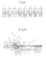
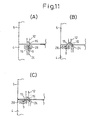
- Fig. 10 is a sectional side view showing a state in which the high frequency IC package is mounted on the high frequency unit 6, and Fig. 11 is a view showing electrical connections in Fig. 10.
- Fig. 10 is a sectional side view showing a state in which the high frequency IC package is mounted on the high frequency unit 6, and Fig. 11 is a view showing electrical connections in Fig. 10.
- the wiring patterns 28, 29 are formed on the upper and the lower face of the circuit board 4 at positions close to the high frequency IC package 5 so that the wiring patterns 28, 29 can be located right above the housing chassis 1.
- the via holes 30 are formed right below the wiring patterns 28 and right above the wiring patterns 29. Both the wiring patterns 28, 29 are connected with each other by the via holes 30. That is, the wiring patterns 29 are formed on a surface of the lower surface of the step portion of the housing chassis 1, and further the wiring patterns 28 are formed right above this portion. Accordingly, the via holes 30 are formed in a portion in which the bypass condensers 9 and the housing chassis 1 are put on each other in the vertical direction.
- the lower electrodes 18 of the bypass condensers 9 are mounted on the wiring patterns 28 on the upper face of the circuit board 4 by the reflow solder 27.
- the upper electrodes 17 of the bypass condensers 9 are connected with the wiring patterns 12 of the high frequency IC package 5 and the wiring patterns 24 of the circuit board 4 by means of the wire bonding connection 15.
- the manufacturing process of the high frequency unit 6 shown in Fig. 10 is the same as that shown in Fig. 9.
- the wiring patterns 12 of the high frequency IC package 5, bypass condensers 9 and wiring patterns 24 of the circuit board 4 can be connected in various ways as shown in Fig. 11.
- Fig. 11(A) shows the same example as that shown in Fig. 10.
- the upper electrodes 17 of the bypass condensers 9 are connected with the wiring patterns 12 of the high frequency IC package 5 and the wiring patterns 24 of the circuit board 4.
- the wiring patterns 12 of the high frequency IC package 5 are connected with the upper electrodes 17 of the bypass condensers 9 and the wiring patterns 24 on the circuit board 4.
- the wiring patterns 24 on the circuit board 4 are connected with the wiring patterns 12 of the high frequency IC package 5 and the upper electrode 17 of the bypass condensers 9.
- Embodiment 3 of the present invention will be explained below.
- points different from the above Embodiment 2 shown in Fig. 10 will be mainly explained, and overlapping explanations are omitted here.
- Fig. 12 is a side view of a state of the high frequency IC package which is mounted on the high frequency unit 6.
- the housing chassis 1 is composed so that the upper end portion 32 of the housing chassis 1 can be exposed from between the high frequency IC package 5 and the circuit board 4.
- the bypass condensers 9, each which is composed as an upper and lower side electrode type single layer ceramic condenser, are mounted on the upper end portion 32 of the housing chassis 1 by means of reflow and fixed by the solder 27.
- the lower electrodes 18 of the bypass condensers 9 are directly grounded. Therefore, it is possible to omit the wiring patterns to be provided between the bypass condenser 9 and the ground.
- the wiring patterns 12 of the high frequency IC package 5, bypass condensers 9 and wiring patterns 24 of the circuit board 4 can be connected in various ways as shown in Fig. 13.
- Fig. 13(A) shows the same example as that shown in Fig. 12.
- the upper electrodes 17 of the bypass condensers 9 are connected with the wiring patterns 12 of the high frequency IC package 5 and the wiring patterns 24 of the circuit board 4.
- the wiring patterns 12 of the high frequency IC package 5 are connected with the upper electrodes 17 of the bypass condensers 9 and the wiring patterns 24 on the circuit board 4.
- the wiring patterns 24 on the circuit board 4 are connected with the wiring patterns 12 of the high frequency IC package 5 and the upper electrodes 17 of the bypass condensers 9.
- the structure of the high frequency IC package and the high frequency unit, into which the high frequency IC package is incorporated can be simplified and downsized.
- the number of processes in the methods of manufacturing the high frequency IC package and the high frequency unit can be reduced.
Landscapes
- Physics & Mathematics (AREA)
- Electromagnetism (AREA)
- Engineering & Computer Science (AREA)
- Microelectronics & Electronic Packaging (AREA)
- Structures For Mounting Electric Components On Printed Circuit Boards (AREA)
Abstract
Description
Claims (20)
- A high frequency IC package comprising:a board;a high frequency IC chip provided and sealed on the board; anda part to determine a characteristic of the high frequency IC chip, provided outside the sealing of the high frequency IC chip.
- A high frequency IC package according to claim 1, wherein the part has electrodes on the upper and lower sides.
- A high frequency IC package according to claim 2, wherein the lower electrode of the part is provided on a wiring pattern formed on the board.
- A high frequency IC package according to claim 3, wherein the part is a coupling condenser, the lower electrode of the part is provided on the wiring pattern on the board, and the upper electrode is connected with another wiring pattern formed on the board by a connecting means.
- A high frequency IC package according to claim 3, wherein the part is a bypass condenser, the lower electrode is provided on one of the bias pattern and the ground pattern formed on the board, and the upper electrode is connected with the bias pattern or the ground pattern formed on the board by a connecting means.
- A high frequency IC package according to claim 1, wherein the part is provided on a face of the board opposite to the face on which the high frequency IC chip is provided.
- A high frequency unit comprising:a high frequency IC package having a high frequency IC chip which is sealed on a board;a circuit board on which a peripheral circuit connected with the high frequency IC package is mounted;a housing chassis on which the circuit board having the high frequency IC package and peripheral circuit is mounted; anda part to determine a characteristic of the high frequency IC chip, provided on the circuit board on which the peripheral circuit is mounted.
- A high frequency unit according to claim 7, wherein the part has electrodes on the upper and lower sides.
- A high frequency unit according to claim 8, wherein the part is a bypass condenser, the lower electrode is provided on a ground pattern formed on a circuit board on which the peripheral circuit is mounted, and the upper electrode is connected with a bias pattern formed on the circuit board, on which the high frequency IC package is mounted, by a connecting means.
- A high frequency unit according to claim 9, further comprising a connecting means for connecting the upper electrode with the peripheral circuit.
- A high frequency unit according to claim 8, wherein the part is a bypass condenser, the lower electrode is provided on a bias pattern formed on a circuit board on which the peripheral circuit is mounted, and the upper electrode is connected with a ground pattern formed on the circuit board on which the high frequency IC package is mounted.
- A high frequency unit according to claim 9, wherein the ground pattern is electrically connected with the housing chassis by the shortest distance through a hole formed on the circuit board on which the peripheral circuit is mounted.
- A high frequency unit according to claim 12, wherein the hole is formed right above the housing chassis and right below the ground pattern.
- A high frequency unit comprising:a high frequency IC package having a high frequency IC chip provided and sealed on a board;a circuit board on which a peripheral circuit connected with the high frequency IC package is mounted;a housing chassis on which the circuit board having the high frequency IC package and peripheral circuit is mounted; anda part to determine a characteristic of the high frequency IC chip, provided on the housing chassis.
- A high frequency unit according to claim 14, wherein the part has electrodes on the upper and lower sides.
- A high frequency unit according to claim 15, wherein the part is a bypass condenser, the lower electrode is provided on the housing chassis, and the upper electrode is connected with a wiring pattern formed on the board on which the high frequency IC package is mounted.
- A high frequency unit according to claim 15, further comprising a connecting means for connecting the upper electrode with the peripheral circuit.
- A high frequency unit comprising:a high frequency IC package having a high frequency IC chip sealed on a board;a circuit board on which a peripheral circuit connected with the high frequency IC package is mounted; anda housing chassis on which the high frequency IC package and the circuit board on which the peripheral circuit is mounted, are mounted, the housing chassis having a step portion for making the height of a surface of the high frequency IC package agree with the height of a surface of the circuit board on which the peripheral circuit is mounted.
- A method of manufacturing a high frequency IC package comprising the steps of:mounting and sealing a high frequency IC chip on a board; andmounting a part to determine a characteristic of the high frequency IC chip on the board.
- A method of manufacturing a high frequency IC package comprising the steps of:mounting a part to determine a characteristic of the high frequency IC chip on a circuit board on which a peripheral circuit connected with a high frequency IC package is mounted, or on a housing chassis; andmounting the high frequency IC package on the circuit board.
Applications Claiming Priority (3)
| Application Number | Priority Date | Filing Date | Title |
|---|---|---|---|
| JP2001301928 | 2001-09-28 | ||
| JP2001301928A JP2003110049A (en) | 2001-09-28 | 2001-09-28 | High-frequency IC package, high-frequency unit using high-frequency IC package, and method of manufacturing the same |
| PCT/JP2001/010103 WO2003032385A1 (en) | 2001-09-28 | 2001-11-19 | High frequency ic package, high frequency unit using it, and method for manufacturing the same |
Publications (2)
| Publication Number | Publication Date |
|---|---|
| EP1432027A1 true EP1432027A1 (en) | 2004-06-23 |
| EP1432027A4 EP1432027A4 (en) | 2009-10-21 |
Family
ID=19122263
Family Applications (1)
| Application Number | Title | Priority Date | Filing Date |
|---|---|---|---|
| EP01982852A Withdrawn EP1432027A4 (en) | 2001-09-28 | 2001-11-19 | HIGH FREQUENCY MICROCIRCUIT HOUSING, HIGH FREQUENCY UNIT USING IT, AND METHOD OF MANUFACTURING THE SAME |
Country Status (5)
| Country | Link |
|---|---|
| US (1) | US7339269B2 (en) |
| EP (1) | EP1432027A4 (en) |
| JP (1) | JP2003110049A (en) |
| KR (1) | KR20030063107A (en) |
| WO (1) | WO2003032385A1 (en) |
Cited By (1)
| Publication number | Priority date | Publication date | Assignee | Title |
|---|---|---|---|---|
| US9711651B2 (en) | 2008-12-26 | 2017-07-18 | Semiconductor Energy Laboratory Co., Ltd. | Semiconductor device and manufacturing method thereof |
Families Citing this family (2)
| Publication number | Priority date | Publication date | Assignee | Title |
|---|---|---|---|---|
| JP2006210480A (en) * | 2005-01-26 | 2006-08-10 | Nec Electronics Corp | Electronic circuit board |
| KR100826695B1 (en) * | 2005-06-30 | 2008-04-30 | 세이코 엡슨 가부시키가이샤 | Integrated circuit device and electronic instrument |
Family Cites Families (20)
| Publication number | Priority date | Publication date | Assignee | Title |
|---|---|---|---|---|
| JPS59124744A (en) * | 1982-12-29 | 1984-07-18 | Fujitsu Ltd | Semiconductor device |
| JPH04142798A (en) * | 1990-10-04 | 1992-05-15 | Toshiba Corp | High frequency device |
| JPH04271161A (en) * | 1991-02-27 | 1992-09-28 | Mitsubishi Electric Corp | Semiconductor device |
| JPH0563136A (en) * | 1991-08-31 | 1993-03-12 | Nec Corp | Hybrid integrated circuit device |
| JPH05211276A (en) * | 1991-12-04 | 1993-08-20 | Nec Corp | Multichip package |
| US5422615A (en) | 1992-09-14 | 1995-06-06 | Hitachi, Ltd. | High frequency circuit device |
| JPH07307412A (en) * | 1994-05-10 | 1995-11-21 | Sumitomo Metal Ind Ltd | Multilayer package with bypass capacitors |
| JP3235452B2 (en) * | 1995-03-20 | 2001-12-04 | 松下電器産業株式会社 | High frequency integrated circuit device |
| JPH0982826A (en) * | 1995-09-18 | 1997-03-28 | Nippon Telegr & Teleph Corp <Ntt> | Package for encapsulating semiconductor element and mounting structure of circuit device using the same |
| JPH09102433A (en) * | 1995-10-05 | 1997-04-15 | Canon Inc | Bypass capacitor and method of forming the same |
| US5796165A (en) | 1996-03-19 | 1998-08-18 | Matsushita Electronics Corporation | High-frequency integrated circuit device having a multilayer structure |
| JPH10135749A (en) * | 1996-10-29 | 1998-05-22 | Nec Corp | High frequency amplifier |
| US6130483A (en) * | 1997-03-05 | 2000-10-10 | Kabushiki Kaisha Toshiba | MMIC module using flip-chip mounting |
| JP3328542B2 (en) * | 1997-03-19 | 2002-09-24 | 富士通株式会社 | High frequency semiconductor integrated circuit device |
| US6057600A (en) * | 1997-11-27 | 2000-05-02 | Kyocera Corporation | Structure for mounting a high-frequency package |
| JP3663953B2 (en) * | 1999-02-24 | 2005-06-22 | 松下電器産業株式会社 | High frequency module and manufacturing method thereof |
| JP3500335B2 (en) * | 1999-09-17 | 2004-02-23 | 株式会社東芝 | High frequency circuit device |
| JP2001185442A (en) * | 1999-12-27 | 2001-07-06 | Murata Mfg Co Ltd | Connection structure and wiring board for multilayer capacitors and decoupling capacitors |
| JP2002164465A (en) * | 2000-11-28 | 2002-06-07 | Kyocera Corp | Wiring boards, wiring boards, their mounting structures, and multi-chip modules |
| JP3896285B2 (en) * | 2002-01-24 | 2007-03-22 | 三菱電機株式会社 | Manufacturing method of semiconductor device |
-
2001
- 2001-09-28 JP JP2001301928A patent/JP2003110049A/en active Pending
- 2001-11-19 KR KR1020027010411A patent/KR20030063107A/en not_active Ceased
- 2001-11-19 EP EP01982852A patent/EP1432027A4/en not_active Withdrawn
- 2001-11-19 US US10/220,409 patent/US7339269B2/en not_active Expired - Fee Related
- 2001-11-19 WO PCT/JP2001/010103 patent/WO2003032385A1/en not_active Ceased
Cited By (3)
| Publication number | Priority date | Publication date | Assignee | Title |
|---|---|---|---|---|
| US9711651B2 (en) | 2008-12-26 | 2017-07-18 | Semiconductor Energy Laboratory Co., Ltd. | Semiconductor device and manufacturing method thereof |
| US11817506B2 (en) | 2008-12-26 | 2023-11-14 | Semiconductor Energy Laboratory Co., Ltd. | Semiconductor device and manufacturing method thereof |
| US12224355B2 (en) | 2008-12-26 | 2025-02-11 | Semiconductor Energy Laboratory Co., Ltd. | Semiconductor device and manufacturing method thereof |
Also Published As
| Publication number | Publication date |
|---|---|
| US7339269B2 (en) | 2008-03-04 |
| EP1432027A4 (en) | 2009-10-21 |
| JP2003110049A (en) | 2003-04-11 |
| US20030094694A1 (en) | 2003-05-22 |
| KR20030063107A (en) | 2003-07-28 |
| WO2003032385A1 (en) | 2003-04-17 |
Similar Documents
| Publication | Publication Date | Title |
|---|---|---|
| EP0595346B1 (en) | Composite microwave module assembly and its connection structure | |
| US5294897A (en) | Microwave IC package | |
| JP3461204B2 (en) | Multi-chip module | |
| EP0580313B1 (en) | Surface mount microcircuit hybrid | |
| US6518501B1 (en) | Electronic part and method of assembling the same | |
| US5426319A (en) | High-frequency semiconductor device including microstrip transmission line | |
| US6046501A (en) | RF-driven semiconductor device | |
| JP4190111B2 (en) | High frequency module | |
| KR100270954B1 (en) | Wire-bond free input/output interface for gaas ics with means of determining known good die | |
| EP0697731B1 (en) | Flat package for semiconductor IC | |
| US7339269B2 (en) | High frequency IC package, high frequency unit using high frequency IC package, and manufacturing method thereof | |
| JP2001189417A (en) | Semiconductor module package | |
| JP3570887B2 (en) | High frequency wiring board | |
| JPH0752759B2 (en) | Package | |
| KR20040063784A (en) | Semiconductor apparatus | |
| US6509633B1 (en) | IC package capable of accommodating discrete devices | |
| JP2836602B2 (en) | Mold type semiconductor device | |
| JP3529323B2 (en) | High frequency unit and method of manufacturing high frequency unit | |
| JP4194896B2 (en) | High frequency unit using high frequency IC package | |
| JPH1093012A (en) | High frequency integrated circuit device | |
| JP2000151222A (en) | High frequency module | |
| JP2004055834A (en) | Hybrid integrated circuit device | |
| JP3640463B2 (en) | MMIC package | |
| JP2643898B2 (en) | Resin-sealed semiconductor device and method of manufacturing the same | |
| JP2775678B2 (en) | High frequency semiconductor integrated circuit device |
Legal Events
| Date | Code | Title | Description |
|---|---|---|---|
| PUAI | Public reference made under article 153(3) epc to a published international application that has entered the european phase |
Free format text: ORIGINAL CODE: 0009012 |
|
| 17P | Request for examination filed |
Effective date: 20020910 |
|
| AK | Designated contracting states |
Kind code of ref document: A1 Designated state(s): AT BE CH CY DE DK ES FI FR GB GR IE IT LI LU MC NL PT SE TR |
|
| A4 | Supplementary search report drawn up and despatched |
Effective date: 20090916 |
|
| RIC1 | Information provided on ipc code assigned before grant |
Ipc: H01L 23/12 20060101ALI20090910BHEP Ipc: H01L 23/66 20060101AFI20090910BHEP Ipc: H01L 23/64 20060101ALI20090910BHEP Ipc: H05K 1/02 20060101ALI20090910BHEP |
|
| 17Q | First examination report despatched |
Effective date: 20100406 |
|
| STAA | Information on the status of an ep patent application or granted ep patent |
Free format text: STATUS: THE APPLICATION IS DEEMED TO BE WITHDRAWN |
|
| 18D | Application deemed to be withdrawn |
Effective date: 20111027 |