EP1432015A2 - Semiconductor and semiconductor substrate, method of manufacturing the same, and semiconductor device - Google Patents
Semiconductor and semiconductor substrate, method of manufacturing the same, and semiconductor device Download PDFInfo
- Publication number
- EP1432015A2 EP1432015A2 EP03028498A EP03028498A EP1432015A2 EP 1432015 A2 EP1432015 A2 EP 1432015A2 EP 03028498 A EP03028498 A EP 03028498A EP 03028498 A EP03028498 A EP 03028498A EP 1432015 A2 EP1432015 A2 EP 1432015A2
- Authority
- EP
- European Patent Office
- Prior art keywords
- defect
- semiconductor
- density
- region
- substrate
- Prior art date
- Legal status (The legal status is an assumption and is not a legal conclusion. Google has not performed a legal analysis and makes no representation as to the accuracy of the status listed.)
- Withdrawn
Links
Images

Classifications
-
- C—CHEMISTRY; METALLURGY
- C30—CRYSTAL GROWTH
- C30B—SINGLE-CRYSTAL GROWTH; UNIDIRECTIONAL SOLIDIFICATION OF EUTECTIC MATERIAL OR UNIDIRECTIONAL DEMIXING OF EUTECTOID MATERIAL; REFINING BY ZONE-MELTING OF MATERIAL; PRODUCTION OF A HOMOGENEOUS POLYCRYSTALLINE MATERIAL WITH DEFINED STRUCTURE; SINGLE CRYSTALS OR HOMOGENEOUS POLYCRYSTALLINE MATERIAL WITH DEFINED STRUCTURE; AFTER-TREATMENT OF SINGLE CRYSTALS OR A HOMOGENEOUS POLYCRYSTALLINE MATERIAL WITH DEFINED STRUCTURE; APPARATUS THEREFOR
- C30B25/00—Single-crystal growth by chemical reaction of reactive gases, e.g. chemical vapour-deposition growth
- C30B25/02—Epitaxial-layer growth
-
- C—CHEMISTRY; METALLURGY
- C30—CRYSTAL GROWTH
- C30B—SINGLE-CRYSTAL GROWTH; UNIDIRECTIONAL SOLIDIFICATION OF EUTECTIC MATERIAL OR UNIDIRECTIONAL DEMIXING OF EUTECTOID MATERIAL; REFINING BY ZONE-MELTING OF MATERIAL; PRODUCTION OF A HOMOGENEOUS POLYCRYSTALLINE MATERIAL WITH DEFINED STRUCTURE; SINGLE CRYSTALS OR HOMOGENEOUS POLYCRYSTALLINE MATERIAL WITH DEFINED STRUCTURE; AFTER-TREATMENT OF SINGLE CRYSTALS OR A HOMOGENEOUS POLYCRYSTALLINE MATERIAL WITH DEFINED STRUCTURE; APPARATUS THEREFOR
- C30B19/00—Liquid-phase epitaxial-layer growth
-
- C—CHEMISTRY; METALLURGY
- C30—CRYSTAL GROWTH
- C30B—SINGLE-CRYSTAL GROWTH; UNIDIRECTIONAL SOLIDIFICATION OF EUTECTIC MATERIAL OR UNIDIRECTIONAL DEMIXING OF EUTECTOID MATERIAL; REFINING BY ZONE-MELTING OF MATERIAL; PRODUCTION OF A HOMOGENEOUS POLYCRYSTALLINE MATERIAL WITH DEFINED STRUCTURE; SINGLE CRYSTALS OR HOMOGENEOUS POLYCRYSTALLINE MATERIAL WITH DEFINED STRUCTURE; AFTER-TREATMENT OF SINGLE CRYSTALS OR A HOMOGENEOUS POLYCRYSTALLINE MATERIAL WITH DEFINED STRUCTURE; APPARATUS THEREFOR
- C30B29/00—Single crystals or homogeneous polycrystalline material with defined structure characterised by the material or by their shape
- C30B29/10—Inorganic compounds or compositions
- C30B29/40—AIIIBV compounds wherein A is B, Al, Ga, In or Tl and B is N, P, As, Sb or Bi
-
- C—CHEMISTRY; METALLURGY
- C30—CRYSTAL GROWTH
- C30B—SINGLE-CRYSTAL GROWTH; UNIDIRECTIONAL SOLIDIFICATION OF EUTECTIC MATERIAL OR UNIDIRECTIONAL DEMIXING OF EUTECTOID MATERIAL; REFINING BY ZONE-MELTING OF MATERIAL; PRODUCTION OF A HOMOGENEOUS POLYCRYSTALLINE MATERIAL WITH DEFINED STRUCTURE; SINGLE CRYSTALS OR HOMOGENEOUS POLYCRYSTALLINE MATERIAL WITH DEFINED STRUCTURE; AFTER-TREATMENT OF SINGLE CRYSTALS OR A HOMOGENEOUS POLYCRYSTALLINE MATERIAL WITH DEFINED STRUCTURE; APPARATUS THEREFOR
- C30B29/00—Single crystals or homogeneous polycrystalline material with defined structure characterised by the material or by their shape
- C30B29/10—Inorganic compounds or compositions
- C30B29/40—AIIIBV compounds wherein A is B, Al, Ga, In or Tl and B is N, P, As, Sb or Bi
- C30B29/403—AIII-nitrides
- C30B29/406—Gallium nitride
-
- H—ELECTRICITY
- H10—SEMICONDUCTOR DEVICES; ELECTRIC SOLID-STATE DEVICES NOT OTHERWISE PROVIDED FOR
- H10P—GENERIC PROCESSES OR APPARATUS FOR THE MANUFACTURE OR TREATMENT OF DEVICES COVERED BY CLASS H10
- H10P14/00—Formation of materials, e.g. in the shape of layers or pillars
- H10P14/20—Formation of materials, e.g. in the shape of layers or pillars of semiconductor materials
- H10P14/29—Formation of materials, e.g. in the shape of layers or pillars of semiconductor materials characterised by the substrates
- H10P14/2901—Materials
- H10P14/2902—Materials being Group IVA materials
- H10P14/2905—Silicon, silicon germanium or germanium
-
- H—ELECTRICITY
- H10—SEMICONDUCTOR DEVICES; ELECTRIC SOLID-STATE DEVICES NOT OTHERWISE PROVIDED FOR
- H10P—GENERIC PROCESSES OR APPARATUS FOR THE MANUFACTURE OR TREATMENT OF DEVICES COVERED BY CLASS H10
- H10P14/00—Formation of materials, e.g. in the shape of layers or pillars
- H10P14/20—Formation of materials, e.g. in the shape of layers or pillars of semiconductor materials
- H10P14/29—Formation of materials, e.g. in the shape of layers or pillars of semiconductor materials characterised by the substrates
- H10P14/2901—Materials
- H10P14/2907—Materials being Group IIIA-VA materials
- H10P14/2911—Arsenides
-
- H—ELECTRICITY
- H10—SEMICONDUCTOR DEVICES; ELECTRIC SOLID-STATE DEVICES NOT OTHERWISE PROVIDED FOR
- H10P—GENERIC PROCESSES OR APPARATUS FOR THE MANUFACTURE OR TREATMENT OF DEVICES COVERED BY CLASS H10
- H10P14/00—Formation of materials, e.g. in the shape of layers or pillars
- H10P14/20—Formation of materials, e.g. in the shape of layers or pillars of semiconductor materials
- H10P14/29—Formation of materials, e.g. in the shape of layers or pillars of semiconductor materials characterised by the substrates
- H10P14/2926—Crystal orientations
-
- H—ELECTRICITY
- H10—SEMICONDUCTOR DEVICES; ELECTRIC SOLID-STATE DEVICES NOT OTHERWISE PROVIDED FOR
- H10P—GENERIC PROCESSES OR APPARATUS FOR THE MANUFACTURE OR TREATMENT OF DEVICES COVERED BY CLASS H10
- H10P14/00—Formation of materials, e.g. in the shape of layers or pillars
- H10P14/20—Formation of materials, e.g. in the shape of layers or pillars of semiconductor materials
- H10P14/34—Deposited materials, e.g. layers
- H10P14/3402—Deposited materials, e.g. layers characterised by the chemical composition
-
- H—ELECTRICITY
- H10—SEMICONDUCTOR DEVICES; ELECTRIC SOLID-STATE DEVICES NOT OTHERWISE PROVIDED FOR
- H10P—GENERIC PROCESSES OR APPARATUS FOR THE MANUFACTURE OR TREATMENT OF DEVICES COVERED BY CLASS H10
- H10P14/00—Formation of materials, e.g. in the shape of layers or pillars
- H10P14/20—Formation of materials, e.g. in the shape of layers or pillars of semiconductor materials
- H10P14/34—Deposited materials, e.g. layers
- H10P14/3402—Deposited materials, e.g. layers characterised by the chemical composition
- H10P14/3404—Deposited materials, e.g. layers characterised by the chemical composition being Group IVA materials
- H10P14/3408—Silicon carbide
-
- H—ELECTRICITY
- H10—SEMICONDUCTOR DEVICES; ELECTRIC SOLID-STATE DEVICES NOT OTHERWISE PROVIDED FOR
- H10P—GENERIC PROCESSES OR APPARATUS FOR THE MANUFACTURE OR TREATMENT OF DEVICES COVERED BY CLASS H10
- H10P14/00—Formation of materials, e.g. in the shape of layers or pillars
- H10P14/20—Formation of materials, e.g. in the shape of layers or pillars of semiconductor materials
- H10P14/34—Deposited materials, e.g. layers
- H10P14/3402—Deposited materials, e.g. layers characterised by the chemical composition
- H10P14/3414—Deposited materials, e.g. layers characterised by the chemical composition being group IIIA-VIA materials
- H10P14/3416—Nitrides
-
- H—ELECTRICITY
- H10—SEMICONDUCTOR DEVICES; ELECTRIC SOLID-STATE DEVICES NOT OTHERWISE PROVIDED FOR
- H10P—GENERIC PROCESSES OR APPARATUS FOR THE MANUFACTURE OR TREATMENT OF DEVICES COVERED BY CLASS H10
- H10P14/00—Formation of materials, e.g. in the shape of layers or pillars
- H10P14/20—Formation of materials, e.g. in the shape of layers or pillars of semiconductor materials
- H10P14/38—Formation of materials, e.g. in the shape of layers or pillars of semiconductor materials characterised by treatments done after the formation of the materials
Definitions
- the present invention relates to semiconductors and semiconductor substrates that can be employed as materials for active semiconductor devices, in particular, for power semiconductor devices and semiconductor light-emitting devices such as LEDs and LDs; methods of manufacturing the same; and semiconductor devices employing these semiconductors
- the breakdown voltage of a semiconductor device is affected by the forbidden energy band gap width (energy band gap), critical breakdown field, and depletion layer width of the semiconductor serving as the material.
- the wider the band gap width and the higher the critical breakdown field of the semiconductor employed as the material the greater the breakdown voltage of the semiconductor device obtained.
- the greater the depletion layer width formed in the active region the greater the breakdown voltage. Since the width of the depletion layer is inversely proportional to the square root of the concentration of impurities such as donors and acceptors that are added to the active region, impurities have been added to adjust the breakdown voltage (see Japanese Unexamined Patent Publication (KOKAI) No. 2002-57109).
- the concentration of impurities added to the active region is reduced.
- the wider the band gap of a semiconductor device the greater the advantage afforded in increasing the breakdown voltage and reducing specific on resistance.
- widening of the band gap width makes it hard to achieve a ohmic contact electrode (ohmic electrode) and reduce contact resistance.
- ohmic electrode ohmic contact electrode
- SBD Schottky barrier diode
- the thickness of the semiconductor device should just be about the width of the depletion layer that can be ensure the desired resistant voltage, and is generally 10 ⁇ m or less.
- a low concentration layer of about 10 ⁇ m is formed on the low resistance substrate of several hundred microns, and a Schottky contact is formed on the surface thereof. Accordingly, when manufacturing power semiconductor devices with high uniformity and controllability, the concentration and thickness uniformity of the low concentration layer formed on the substrate are important. Further, in order to reduce specific on resistance as low as possible, it is necessary to increase the doping concentration of the substrate as high as possible.
- the present invention relates to semiconductors and semiconductor substrates for obtaining semiconductor devices that exhibit little power loss while affording improved breakdown voltage and light-emitting efficiency; methods of manufacturing the same; and semiconductor devices employing these semiconductors.
- the present invention provides:
- the semiconductor of the present invention is characterized by consisting of a compound single crystal and comprising a high-defect-density region having a planar defect density of 1 x 10 7 /cm 2 or more and a low-defect-density region having a planar defect density of 1/cm 2 or less.
- the semiconductor of the present invention may also be a semiconductor that has a plate shape having at least one pair of opposite surfaces that are roughly parallel, on one surface (high-defect-density surface) of which, the high-defect-density region having a planar defect density of 1 x 10 7 /cm 2 or more is exposed, and, on the other surface (low-defect-density surface) of which, the low-defect-density region having a planar defect density of 1/cm 2 or less is exposed.
- the present invention also relates to a semiconductor substrate wherein the semiconductor of the present invention is provided on a substrate.
- the semiconductor of the present invention permits the obtaining of a ohmic contact with low resistance irrespective of the impurities incorporated. Further, by having a region with a low concentration of planar defects (low-defect-density region) imparting a reduction in breakdown voltage and an increase in leak current, the semiconductor of the present invention permits the obtaining of a power semiconductor device affording a high breakdown voltage keeping high efficiency. In particular, since planar defects can be reduced or eliminated not by annihilation of planar defects in the semiconductor of the present invention, planar defects can be reduced if the film thickness becomes thinner.
- the interface between the low resistivity region (high-defect-density region) and the high resistivity region (low-defect-density region) can be made steep, and it is also possible to fabricate power semiconductor devices of high controllability and uniformity since impurities do not diffuse to the out-side and the memory effect during growth does not occur. Further, since an ohmic contact is obtained through defects, an advantage is afforded in that there is less dependence on temperature.
- the planar defect density in the high-defect-density region is 1 x 10 7 /cm 2 or more, preferably 1 x 10 9 /cm 2 or more, and more preferably 1 x 10 10 /cm 2 or more.
- the planar defect density is less than 1 x 10 7 /cm 2 , the resistivity of the region containing defects does not become one tenth or less of that of the region not containing defects, and the specific on resistance of the device does not decrease.
- the planar defect density in the low-defect-density region is 1/cm 2 or less, preferably 0.1/cm 2 or less, and more preferably 0.01/cm 2 or less.
- planar defect density exceeds 1/cm 2 , the leakage current in that region increases, precluding the achievement of good device characteristics.
- planar defect density can be measured as follows; etch-pits are formed on spots on the surface of which defects has been exposed by etching using molten KOH or the like, and then the number of these etch pits is counted using a microscope to measure the planar defect density.
- the high-density defect region preferably has an electron concentration of 10 times or more, more preferably 100 times or more of that of the low-defect-density region at room temperature.
- the specific on resistance of the device can be decreased.
- the semiconductor of the present invention can be comprised of a group IV-IV compound single crystal, a group III-V compound single crystal, or a group II-VI compound single crystal.
- Specific examples are compound single crystals such as GaAs, AlAs, InAs, GaP, GaSb, InP, InSb, ZnS, ZnSe, CdS, CdTe, and HgTe.
- the semiconductor of the present invention is preferably a crystal having planar defects extending in a plane not perpendicular to the orientation of crystal growth. Cubic crystals are examples of such crystals.
- Examples of the compound single crystals constituting the semiconductor of the present invention are cubic silicon carbide (SiC), gallium nitride (GaN), indium phosphide (InP), gallium arsenide (GaAs), indium arsenide (InAs), aluminum arsenide (AlAs), and alloy crystals thereof.
- the planar defect contained in the semiconductor of the present invention can be at least one of anti-phase boundary (APB), stacking fault (SF), and small-angle grain boundary (SAGB).
- APB anti-phase boundary
- SF stacking fault
- SAGB small-angle grain boundary
- planes having such planar defects are suitable as a plane on the substrate side and as an ohmic contact layer.
- the boundary between the low resistivity region (high-defect-density region) and the high resistivity region (low-defect-density region) can be set as desired only with the crystal growth step. Based on the position at which the boundary is inserted, the breakdown voltage of the device can be set as desired.
- the gradient of the crystal defect density is preferably 4 x 10 9 /cm 3 or more.
- the breakdown voltage and resistivity of the device can be readily set by forming a region in which the planar defect density greatly changes at a desired position.
- the method of manufacturing the semiconductor of the present invention will be described in greater detail below.
- the semiconductor of the present invention can be obtained by sequentially epitaxially growing, on a growth substrate, two or more layers consisting of a compound single crystal either identical to or different from a compound single crystal constituting the substrate from vapor phase or liquid phase.
- a high-defect-density region having a planar defect of 1 x 10 7 /cm 2 or more can be formed on a growth substrate by growing a single crystal having a lattice constant different from that of the single crystal constituting the growth substrate. Further, by skewing the normal axis of the growth substrate to a specific orientation (for example, [110] orientation) relative to a specific crystal plane (for example, (001) face), it is possible to converge planar defects in a single direction and, independent on the film thickness, cause the planar defects to propagate in parallel at a density of 1 x 10 7 /cm 2 or more. Thus, it is possible to grow a crystal while constantly exposing the planar defect on the surface to propagate the structure of the planar defect.
- a specific orientation for example, [110] orientation
- a specific crystal plane for example, (001) face
- the planar defect density can be controlled by changing the supersaturation.
- changing the supersaturation when growing crystals permits the formation of a layer with a planar defect density of 1 x 10 7 /cm 2 or more on a substrate.
- a low-defect-density region having a planar defect of 1/cm 2 or less can be formed by growing a base crystal in an orientation differing from an orientation of propagation of the structure of the planar defect exposed on the surface of the aforementioned high-defect-density region to terminate the propagation of planar defect on the growth surface.
- the angle between the orientation of the planar defect propagation and the orientation of the base crystal propagation is preferably 10 degrees or more. When this angle is 10 degrees or more, the planar defects are sealed off over as limited a region as possible, and it is possible to terminate the planar defects.
- a method of processing the film surface during growth to render it uneven, and then growing a base crystal in an orientation differing from an orientation of the planar defect propagation, or to employ a method of selectively forming on the surface of the planar defects a mask obstructing the propagation of the planar defects.
- Specific examples of methods that can be employed are forming facets, undulations, or groove-like holes, or etch-pits on the surface of the high-defect-density region.
- the present invention it is possible to directly provide a low-defect-density region on a high-defect-density region.
- a region (transition region) having a gradient of defect density of 4 x 10 9 /cm 3 or more between the high-defect-density region and the low-defect-density region.
- the transition region preferably has a thickness of 5 ⁇ m or less, more preferably 1 ⁇ m or less.
- the gradient of defect density can be obtained as a change in the etch-pit density (differential value) relative to the amount of grinding by counting the number of etching pits while gradually grinding the surface.
- facets, undulations, and the like there are numerous examples of methods of forming facets, undulations, and the like, such as photolithographic techniques, press processing techniques, laser processing techniques, ultrasonic processing techniques, and grinding techniques.
- the planar defect propagating in the high-defect-density region should just have a shape sufficient to be reduced or eliminated effectively in the low-defect-density region.
- facets or the like of a desired shape can be transferred to the surface of the high-defect-density surface by forming a mask pattern to be transferred to the surface of the high-defect-density surface as desired. For example, by varying the line width of the pattern, it is possible to control the width of the shape of facets or the like.
- etching ratio between a resist and a substrate, it is possible to control the depth and angle of slope thereof. Even when a rectangular pattern is undesirable, it is possible to transfer a pattern to a resist, reflow of the resist by heating, and form a wave-shaped pattern.
- a press processing technique it is possible to form facets or the like of a desired shape on the growth surface by forming a pressing mold to a desired shape. By forming molds of various shapes, it is possible to form facets or the like of various shapes on the growth substrate.
- a laser processing or ultrasonic processing technique since it is possible to directly form a shape such as a facet on the substrate, more minute processing is possible.
- grinding processing varying the size of abrasives and pressure of the grinding makes it possible to control the width and depth of the undulating shape. When forming facets or undulations in only one direction, grinding is conducted in only one direction.
- the edge of the facets should be as close as possible to parallel to the planar defects, and the planar defects are desirably positioned at the bottom of the facets.
- the planar defects are desirably positioned at the bottom of the facets.
- conditions causing the facets to grow to the direction as close as possible to perpendicular to the normal direction of the substrate are desirably employed.
- adjacent facets are desirably opposed.
- a high-defect-density region on a growth substrate and then forming a low-defect-density region during crystal growth has been described.
- the present invention includes the aspect of forming a low-defect-density region and then forming a high-defect-density region.
- a high-defect-density region can be formed on a low-defect-density region by forming a low-defect-density region on a growth substrate, followed by growing a crystal while greatly altering the crystal growth condition to increase the two-dimensional nucleation probability of planar defects.
- the semiconductor of the present invention can be employed after the growth substrate is molten by annealing, for example, and then eliminated following finishing the crystal growth. Alternatively, the semiconductor of the present invention can be employed without eliminating the growth substrate.
- the semiconductor of the present invention can be formed by bonding together a high-defect-density film and a low-defect-density film.
- OH-groups can be formed on both the low-defect-density surface and high-defect-density surface by the treatment with hydrogen peroxide and sulfuric acid, the two surfaces can then be adhered by Van der Waals forces, and then a heat treatment of 1,600°C or more can be applied, for example, to diffuse the O atoms at the interface, yielding a strong continuous interface.
- a semiconductor device comprising an electrode having at least one ohmic contact and an electrode having at least one non-ohmic contact can be obtained by forming the ohmic contact in the high-density defect region of the semiconductor of the present invention and forming the non-ohmic contact in the low-density defect region thereof.
- semiconductor devices employing the semiconductor of the present invention are Schottky barrier diodes, MOS-FETs, MES-FETs, IGBTs, GTOs, thyristors, pressure sensors, UV sensors, and infrared sensors.
- Cubic silicon carbide (3C-SiC) was heteroepitaxially grown under the conditions given in Table 1 on a Si (001) substrate having a normal axis inclined by 1 to 4° toward [110] orientation.
- the stacking faults were converged in a single direction by the effect of the incline of the normal axis, and irrespective of thickness, the stacking faults propagated parallel to (111) face at a density of 1 x 10 7 to 1 x 10 10 /cm 2 .
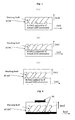
- the distribution of stacking faults in this process is schematically shown in Fig. 1(a).
- Facets inclined by 4 to 8 ° toward [-1, -1, 0] orientation were formed in a manner covering the growth surface (Fig. 1(b)).
- the facets were formed at a spacing of 70 ⁇ m and processing was conducted to yield a sawtooth shaped cross-section. The height of irregularities of the cross-section were about 5 ⁇ m. Partial grinding with diamond abrasives was conducted to form facets.
- 3C-SiC was then again grown on this surface under the conditions shown in Table 1 (secondary growth). This secondary growth yielded transverse crystal growth to [-1, -1, 0] orientation, and, as shown in Fig.
- the electron concentration of the high-defect-density region of this semiconductor was 10 19 /cm 3 and the electron concentration of the low-defect-density region was 10 15 /cm 3 .
- Ni was evaporated to a thickness of 3,000 ⁇ over the entire initially grown surface (the surface that had been in contact with the Si substrate up to this point), and a Ni electrode 3,000 ⁇ in thickness with a diameter of 300 ⁇ m was formed on the surface that had been subjected to secondary growth (Fig. 2).
- the Ni electrode on the initially grown surface side exhibited ohmic characteristics. It had a contact resistance of 1 x 10 -7 /cm 2 .
- the Ni electrode of the secondary growth surface exhibited non-ohmic characteristics; it exhibited a barrier height of 1.2 eV.
- the breakdown voltage of the device varied with the thickness of the secondary growth layer.
- the Schottky barrier diode produced by the present method despite not having an impurity profile, permitted control of the breakdown voltage through the thickness of the secondary growth layer. Relation between secondary growth layer thickness and breakdown voltage Thickness of secondary growth layer ( ⁇ m) Breakdown voltage(V) 2 3 3 39 4 83 5 120 7 470 10 690 15 720 19 720 25 720 30 720
- 3C-SiC was grown on a Si (001) substrate under the conditions in Table 1.
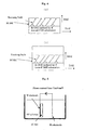
- antiphase boundaries and stacking faults propagating parallel to ⁇ 111 ⁇ faces occurred (Fig. 3(a)).
- the density of the stacking faults and antiphase boundaries varied with the thickness of the 3C-SiC, and it was 7 x 10 8 /cm 2 for a thickness of about 100 ⁇ m.
- facets inclined by 4 ° toward [-110] orientation were provided on the surface.
- the facets were formed at a spacing of 70 ⁇ m and processed to form a sawtooth-shaped cross-section (Fig. 3(b)).
- the height of irregularities of the cross-section were about 5 ⁇ m.
- the facets were formed at a spacing of 70 ⁇ m and processed to form a sawtooth-shaped cross-section.
- the height of irregularities of the cross-section were about 5 ⁇ m.
- 3C-SiC was again grown on this surface (tertiary growth), imparting transverse crystal growth to [ 110] orientation due to the effect of the inclined surface, terminating the stacking faults (Fig. 3(e)).
- the thickness of the region in which the stacking faults were terminated was 5 ⁇ m or less.
- the gradient of planar defect density was 6 x 10 11 /cm 3 .
- the electron concentration of the high-defect-density region of this semiconductor was 10 19 /cm 3
- the electron concentration of the low-defect-density region was 10 15 /cm 3
- Differential Hall measurement revealed the resistivity of the tertiary growth layer to be 130 ⁇ -cm. Further, as is also clear from the results of Example 1, when a diode was prepared from the semiconductor of the present Example, it was possible to control the breakdown voltage of the diode through the thickness of the tertiary growth layer.
- Cubic silicon carbide (3C-SiC) was heteroepitaxially grown under the conditions in Table 1 on a Si (001) substrate having a normal axis inclined by 1 to 4° toward [110] orientation.
- high-density stacking faults occurred at the 3C-SiC/Si interface due to a difference in lattice constants.
- the stacking faults were converged in a single direction due to the effect of the incline of the normal axis, propagating in parallel to (111) face with a density of 1 x 10 7 to 1 x 10 10 /cm 2 irrespective of film thickness.
- the distribution of the stacking faults in this process was as shown in Fig. 1(a).
- the thickness of the region in which the stacking faults were terminated was limited to equal to or less than 5 ⁇ m, that was a depth of the grooves.
- the electron concentration of the high-defect-density region of this semiconductor was 10 19 /cm 3 and the electron concentration of the low-defect-density region was 10 15 /cm 3 .
- Differential Hall measurement revealed the resistivity of the secondary growth layer to be 130 ⁇ -cm.
- Cubic silicon carbide (3C-SiC) was heteroepitaxially grown under the conditions in Table 1 on a Si (001) substrate having a normal axis inclined by 1 to 4° toward [110] orientation.
- high-density stacking faults occurred at the 3C-SiC/Si interface due to a difference in lattice constants.
- the stacking faults were converged in a single direction due to the effect of the incline of the normal axis, propagating in parallel to the (111) face with a density of 1 x 10 7 to 1 x 10 10 /cm 2 irrespective of film thickness.
- the distribution of the stacking faults in this process was as shown in Fig. 1.
- the Si substrate was selectively etched away with a HF+HNO 3 solution to obtain free-standing 3C-SiC.
- W was then vapor-deposited to a thickness of 3,000 ⁇ over the entire surface of the initially grown surface (the surface that had been in contact with the Si substrate up to this point).
- the 3C-SiC substrate was immersed in 50 % HF solution, an opposing Pt mesh electrode was provided at a spot 1 cm away from the surface.
- the rear surface W electrode was made the cathode, the Pt electrode was made the anode, and DC current was made to flow with a current density of 1 mA/cm 2 to etch the 3C-SiC surface (Fig. 5).
- planar defect propagation parallel to (111) face was blocked by the base crystal growing to [-1,-1,0] and [110] orientations, eliminating stacking faults at a density gradient of 2 x 10 9 /cm 3 or more.
- the thickness of the region in which the stacking faults were terminated was limited to equal to or less than 5 ⁇ m, that was a depth of the grooves.
- the electron concentration of the high-defect-density region of this semiconductor was 10 19 /cm 3 and the electron concentration of the low-defect-density region was 10 15 /cm 3 .
- Differential Hall measurement revealed the resistivity of the secondary growth layer to be 130 ⁇ -cm.
- a Cold-wall type MOCVD system was employed to heteroepitaxially grow cubic gallium nitride (c-GaN) to a thickness of 30 ⁇ m on a GaAs (001) substrate under the conditions of Table 3.
- c-GaN cubic gallium nitride
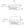
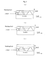
- Table 3 high-density stacking faults generated due to a difference in lattice constants at the c-GaN/GaAs interface (Fig. 7(a)).
- the stacking fault density was 3.5 x 10 9 /cm 2 .
- SiC growth condition in Example 5 Temperature of substrate 1200 °C Pressure 1.5 Torr HN 3 flow rate 50 sccm TMG flow rate 5 sccm H 2 flow rate 1 slm
- etch-pits were then homoepitaxially grown again under the conditions shown in Fig. 3 (secondary growth).
- the propagation of stacking faults parallel to ⁇ 111 ⁇ faces was terminated and the stacking fault density became zero in a region of equal to or less than 5 ⁇ m, that was a depth of etch-pits (Fig. 7(c)).
- the density gradient of the stacking faults was 7 x 10 12 /cm 3 .
- the electron concentration of the high-defect-density region of this semiconductor was 4 x 10 18 /cm 3 and the electron concentration of the low-defect-density region was 8 x 10 14 /cm 3 .
- annealing was conducted for one hour at 1,200 °C to melt and remove the GaAs substrate.
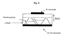
- a Ge-doped Au electrode was formed over the entire surface formed on the GaAs substrate side, and a Pt electrode 3,000 ⁇ in thickness and 300 ⁇ m in diameter was formed on the side where the secondary growth had been conducted (Fig. 8).
- the Au electrode on the GaAs substrate side exhibited ohmic characteristics, having a contact resistance of 1.4 x 10 - 8 /cm 2 . Further, the Pt electrode on the secondary growth surface exhibited non-ohmic characteristics, having a barrier height of 0.54 eV.
- the breakdown voltage of the device varied with the thickness of the secondary growth layer. As shown in Table 4, the Schottky barrier diode prepared by this method, despite not having an impurity profile, permitted the control of the breakdown voltage through the thickness of the secondary growth layer. Relation between secondary growth layer thickness and breakdown voltage Thickness of secondary growth layer ( ⁇ m) Breakdown voltage (V) 1 0.5 2 3 3 21 4 58 5 141 7 240 10 270
- the present invention is not limited to compound semiconductors thereof, and is effective for group IV-IV compound single crystals, group III-V compound single crystals, and group II-VI compound single crystals.
- the type of defect is not limited to stacking faults; the same effect can be achieved with antiphase boundaries and small-angle grain boundaries, so long as crystal growth to an orientation differing from the propagation orientation of the defects is used to block defect propagation.
- the growth method is not limited to vapor phase growth; the same effect can be achieved by liquid phase growth.
- a semiconductor having a high breakdown voltage and being suitable for use in a semiconductor device and a semiconductor device employing this semiconductor.
Landscapes
- Chemical & Material Sciences (AREA)
- Engineering & Computer Science (AREA)
- Crystallography & Structural Chemistry (AREA)
- Materials Engineering (AREA)
- Metallurgy (AREA)
- Organic Chemistry (AREA)
- Inorganic Chemistry (AREA)
- Chemical Kinetics & Catalysis (AREA)
- General Chemical & Material Sciences (AREA)
- Recrystallisation Techniques (AREA)
- Electrodes Of Semiconductors (AREA)
- Crystals, And After-Treatments Of Crystals (AREA)
Abstract
Description
In particular, the present invention relates to semiconductors and semiconductor substrates for obtaining semiconductor devices that exhibit little power loss while affording improved breakdown voltage and light-emitting efficiency; methods of manufacturing the same; and semiconductor devices employing these semiconductors. Specifically, the present invention provides:
growing a compound single crystal having a planar defect at a density of 1 x 10⁷/cm2 or more on the surface of the growth substrate(referred to as "step (A)", hereinafter), and
growing a compound single crystal in an orientation differing from an orientation of propagation of the planar defect exposed on the surface of the compound single crystal grown in the step (A) to form a compound single crystal layer having a planar defect density of 1/cm2 or less (referred to as "step (B)", hereinafter);
The present invention also relates to a semiconductor substrate wherein the semiconductor of the present invention is provided on a substrate.
Further, by having a region with a low concentration of planar defects (low-defect-density region) imparting a reduction in breakdown voltage and an increase in leak current, the semiconductor of the present invention permits the obtaining of a power semiconductor device affording a high breakdown voltage keeping high efficiency. In particular, since planar defects can be reduced or eliminated not by annihilation of planar defects in the semiconductor of the present invention, planar defects can be reduced if the film thickness becomes thinner.
Accordingly, the interface between the low resistivity region (high-defect-density region) and the high resistivity region (low-defect-density region) can be made steep, and it is also possible to fabricate power semiconductor devices of high controllability and uniformity since impurities do not diffuse to the out-side and the memory effect during growth does not occur. Further, since an ohmic contact is obtained through defects, an advantage is afforded in that there is less dependence on temperature.
etch-pits are formed on spots on the surface of which defects has been exposed by etching using molten KOH or the like, and then the number of these etch pits is counted using a microscope to measure the planar defect density.
In the semiconductor of the present invention, the breakdown voltage and resistivity of the device can be readily set by forming a region in which the planar defect density greatly changes at a desired position. Further, it is possible to obtain a low resistance contact layer and a low-defect-density high resistivity active layer only with a process of manufacturing a semiconductor substrate without an impurity addition step such as ion implantation or thermal diffusion, permitting enhanced yields and cost reductions.
The semiconductor of the present invention can be obtained by sequentially epitaxially growing, on a growth substrate, two or more layers consisting of a compound single crystal either identical to or different from a compound single crystal constituting the substrate from vapor phase or liquid phase.
Further, by skewing the normal axis of the growth substrate to a specific orientation (for example, [110] orientation) relative to a specific crystal plane (for example, (001) face), it is possible to converge planar defects in a single direction and, independent on the film thickness, cause the planar defects to propagate in parallel at a density of 1 x 10⁷/cm2 or more. Thus, it is possible to grow a crystal while constantly exposing the planar defect on the surface to propagate the structure of the planar defect.
| SiC growth condition in Example 1 | |
| Temperature of substrate | 1320 °C |
| Pressure | 1.3 Torr |
| SiH4 flow rate | 50 sccm |
| C3H8 flow rate | 34 sccm |
| H2 flow rate | 3 slm |
Finally, the Si substrate was selectively eliminated with a HF+HNO3 solution to obtain free-standing 3C-SiC. The electron concentration of the high-defect-density region of this semiconductor was 1019/cm3 and the electron concentration of the low-defect-density region was 1015/cm3. Next, Ni was evaporated to a thickness of 3,000 Å over the entire initially grown surface (the surface that had been in contact with the Si substrate up to this point), and a Ni electrode 3,000 Å in thickness with a diameter of 300 µm was formed on the surface that had been subjected to secondary growth (Fig. 2). The Ni electrode on the initially grown surface side exhibited ohmic characteristics. It had a contact resistance of 1 x 10⁻⁷/cm2. Further, the Ni electrode of the secondary growth surface exhibited non-ohmic characteristics; it exhibited a barrier height of 1.2 eV. The breakdown voltage of the device varied with the thickness of the secondary growth layer. As shown in Table 2, the Schottky barrier diode produced by the present method, despite not having an impurity profile, permitted control of the breakdown voltage through the thickness of the secondary growth layer.
| Relation between secondary growth layer thickness and breakdown voltage | |
| Thickness of secondary growth layer (µm) | Breakdown voltage(V) |
| 2 | 3 |
| 3 | 39 |
| 4 | 83 |
| 5 | 120 |
| 7 | 470 |
| 10 | 690 |
| 15 | 720 |
| 19 | 720 |
| 25 | 720 |
| 30 | 720 |
| SiC growth condition in Example 5 | |
| Temperature of substrate | 1200 °C |
| Pressure | 1.5 Torr |
| HN3 flow rate | 50 sccm |
| TMG flow rate | 5 sccm |
| H2 flow rate | 1 slm |
| Relation between secondary growth layer thickness and breakdown voltage | |
| Thickness of secondary growth layer (µm) | Breakdown voltage (V) |
| 1 | 0.5 |
| 2 | 3 |
| 3 | 21 |
| 4 | 58 |
| 5 | 141 |
| 7 | 240 |
| 10 | 270 |
Claims (13)
- A semiconductor which consists of a compound single crystal and comprises a region (referred to as "high-defect-density region", hereinafter) having a planar defect density of 1 x 10⁷/cm2 or more and a region (referred to as "low-defect-density region", hereinafter) having a planar defect density of 1/cm2 or less.
- The semiconductor according to claim 1, wherein the high-density defect region has an electron concentration of 10 times or more of that of the low-defect-density region at room temperature.
- The semiconductor according to claim 1 or 2, wherein the semiconductor has a plate shape having at least one pair of opposite surfaces that are roughly parallel, on one surface (referred to as "high-defect-density surface", hereinafter) of which, the high-defect-density region is exposed, and, on the other surface (referred to as "low-defect-density surface", hereinafter) of which, the low-defect-density region is exposed.
- The semiconductor according to any of claims 1 to 3, wherein the planar defect is at least one of anti-phase boundary, stacking fault, and small-angle grain boundary.
- The semiconductor according to any of claims 1 to 4, wherein the compound single crystal is a group IV-IV compound single crystal, a group III-V compound single crystal, or a group II-VI compound single crystal.
- The semiconductor according to any of claims 1 to 5, wherein the compound single crystal is a cubic type crystal.
- The semiconductor according to any of claims 1 to 6, wherein the semiconductor has a transition region, between the high-defect-density region and the low-defect-density region, having a thickness of 5 µm or less and a gradient of defect density of 4 x 10⁹/cm3 or more.
- A semiconductor substrate, wherein the semiconductor according to any of claims 1 to 7 is provided on a substrate.
- The semiconductor substrate according to claim 8, wherein the semiconductor comprises a high-defect-density region and a low-defect-density region in this order on a substrate.
- A method of manufacturing the semiconductor according to any of claims 1 to 7 or the semiconductor substrate according,to claim 8 or 9, in which a compound single crystal is grown on a substrate using liquid phase or vapor phase, and the method comprises the steps of;
growing a compound single crystal having a planar defect at a density of 1 x 10⁷/cm2 or more on the surface of the growth substrate(referred to as "step (A)", hereinafter), and
growing a compound single crystal in an orientation differing from an orientation of propagation of the planar defect exposed on the surface of the compound single crystal grown in the step (A) to form a compound single crystal layer having a planar defect density of 1/cm2 or less (referred to as "step (B)", hereinafter). - The method according to claim 10, wherein the step (A) is carried out by generating a planar defect at a density of 1 x 10⁷/cm2 or more on the surface of the substrate as well as constantly exposing the planar defect on the surface to propagate the structure of the planar defect.
- The method according to claim 10 or 11, wherein, following forming the compound single crystal layer having a planar defect density of 1/cm2 or less, the growth substrate is removed to obtain the semiconductor according to any of claims 1 to 7.
- A semiconductor device comprising the semiconductor according to any of claims 1 to 7, an electrode having at least one ohmic contact, and an electrode having at least one non-ohmic contact, wherein the ohmic contact is formed in the high-density defect region of the semiconductor and the non-ohmic contact is formed in the low-density defect region of the semiconductor.
Applications Claiming Priority (2)
| Application Number | Priority Date | Filing Date | Title |
|---|---|---|---|
| JP2002364009 | 2002-12-16 | ||
| JP2002364009A JP4856350B2 (en) | 2002-12-16 | 2002-12-16 | diode |
Publications (2)
| Publication Number | Publication Date |
|---|---|
| EP1432015A2 true EP1432015A2 (en) | 2004-06-23 |
| EP1432015A3 EP1432015A3 (en) | 2009-11-11 |
Family
ID=32376211
Family Applications (1)
| Application Number | Title | Priority Date | Filing Date |
|---|---|---|---|
| EP03028498A Withdrawn EP1432015A3 (en) | 2002-12-16 | 2003-12-12 | Semiconductor and semiconductor substrate, method of manufacturing the same, and semiconductor device |
Country Status (3)
| Country | Link |
|---|---|
| US (1) | US7164187B2 (en) |
| EP (1) | EP1432015A3 (en) |
| JP (1) | JP4856350B2 (en) |
Cited By (2)
| Publication number | Priority date | Publication date | Assignee | Title |
|---|---|---|---|---|
| CN102822395A (en) * | 2010-03-29 | 2012-12-12 | 爱沃特株式会社 | Method for manufacturing single crystal 3C-SiC substrate and single crystal 3C-SiC substrate obtained by the method |
| GB2542788A (en) * | 2015-09-29 | 2017-04-05 | Univ Warwick | 3C-SiC based sensor |
Families Citing this family (14)
| Publication number | Priority date | Publication date | Assignee | Title |
|---|---|---|---|---|
| US20060011906A1 (en) * | 2004-07-14 | 2006-01-19 | International Business Machines Corporation | Ion implantation for suppression of defects in annealed SiGe layers |
| JP2006073770A (en) * | 2004-09-02 | 2006-03-16 | Namiki Precision Jewel Co Ltd | Epitaxial growth substrate manufacturing method |
| US7391058B2 (en) * | 2005-06-27 | 2008-06-24 | General Electric Company | Semiconductor devices and methods of making same |
| JP2007027630A (en) * | 2005-07-21 | 2007-02-01 | Kansai Electric Power Co Inc:The | Bipolar semiconductor device and manufacturing method thereof |
| TWI293805B (en) * | 2006-01-24 | 2008-02-21 | Ind Tech Res Inst | Ultraviolet detector |
| JP4503060B2 (en) * | 2007-09-21 | 2010-07-14 | Okiセミコンダクタ株式会社 | UV sensor, UV sensor setting method |
| JP2010184833A (en) * | 2009-02-12 | 2010-08-26 | Denso Corp | Silicon carbide single crystal substrate and silicon carbide single crystal epitaxial wafer |
| JP5345499B2 (en) * | 2009-10-15 | 2013-11-20 | Hoya株式会社 | Compound single crystal and method for producing the same |
| JP2011258768A (en) * | 2010-06-09 | 2011-12-22 | Sumitomo Electric Ind Ltd | Silicon carbide substrate, substrate with epitaxial layer, semiconductor device and method of manufacturing silicon carbide substrate |
| WO2012157670A1 (en) * | 2011-05-18 | 2012-11-22 | Hoya株式会社 | Silicon carbide substrate |
| TWI528580B (en) | 2012-03-30 | 2016-04-01 | 聖戈班晶體探測器公司 | Method of forming a freestanding semiconductor wafer |
| US9275861B2 (en) | 2013-06-26 | 2016-03-01 | Globalfoundries Inc. | Methods of forming group III-V semiconductor materials on group IV substrates and the resulting substrate structures |
| DE102022113729B4 (en) | 2022-01-21 | 2025-09-11 | Infineon Technologies Ag | SEMICONDUCTOR DEVICE WITH METAL NITRIDE LAYER AND A METHOD FOR MANUFACTURING THE SAME |
| US20240332366A1 (en) * | 2023-03-31 | 2024-10-03 | Stmicroelectronics International N.V. | Polycrystalline silicon carbide substrate with density gradient and method of manufacturing the same |
Citations (1)
| Publication number | Priority date | Publication date | Assignee | Title |
|---|---|---|---|---|
| JP2000178790A (en) | 1998-12-11 | 2000-06-27 | Kobe Steel Ltd | Anodic oxide film-coated member excellent in resistances to thermal cracking and corrosion |
Family Cites Families (10)
| Publication number | Priority date | Publication date | Assignee | Title |
|---|---|---|---|---|
| JP3230650B2 (en) * | 1996-03-27 | 2001-11-19 | 富士電機株式会社 | Silicon carbide semiconductor substrate, method of manufacturing the same, and silicon carbide semiconductor device using the substrate |
| JP3880717B2 (en) | 1997-12-19 | 2007-02-14 | Hoya株式会社 | Method for producing silicon carbide |
| US6608327B1 (en) * | 1998-02-27 | 2003-08-19 | North Carolina State University | Gallium nitride semiconductor structure including laterally offset patterned layers |
| EP1130135B1 (en) * | 1999-10-08 | 2007-08-08 | Hoya Corporation | Silicon carbide film and method for manufacturing the same |
| JP3576432B2 (en) | 1998-10-10 | 2004-10-13 | Hoya株式会社 | Silicon carbide film and method of manufacturing the same |
| JP4032538B2 (en) * | 1998-11-26 | 2008-01-16 | ソニー株式会社 | Semiconductor thin film and semiconductor device manufacturing method |
| US6475456B2 (en) * | 2000-02-29 | 2002-11-05 | Hoya Corporation | Silicon carbide film and method for manufacturing the same |
| JP4563609B2 (en) * | 2000-04-07 | 2010-10-13 | Hoya株式会社 | Method for producing silicon carbide |
| JP3650727B2 (en) | 2000-08-10 | 2005-05-25 | Hoya株式会社 | Silicon carbide manufacturing method |
| JP3754294B2 (en) * | 2000-12-28 | 2006-03-08 | 株式会社東芝 | Method for manufacturing silicon carbide single crystal substrate and method for manufacturing semiconductor device |
-
2002
- 2002-12-16 JP JP2002364009A patent/JP4856350B2/en not_active Expired - Fee Related
-
2003
- 2003-12-09 US US10/729,983 patent/US7164187B2/en not_active Expired - Fee Related
- 2003-12-12 EP EP03028498A patent/EP1432015A3/en not_active Withdrawn
Patent Citations (1)
| Publication number | Priority date | Publication date | Assignee | Title |
|---|---|---|---|---|
| JP2000178790A (en) | 1998-12-11 | 2000-06-27 | Kobe Steel Ltd | Anodic oxide film-coated member excellent in resistances to thermal cracking and corrosion |
Cited By (4)
| Publication number | Priority date | Publication date | Assignee | Title |
|---|---|---|---|---|
| CN102822395A (en) * | 2010-03-29 | 2012-12-12 | 爱沃特株式会社 | Method for manufacturing single crystal 3C-SiC substrate and single crystal 3C-SiC substrate obtained by the method |
| EP2554718A4 (en) * | 2010-03-29 | 2014-01-08 | Air Water Inc | METHOD FOR MANUFACTURING SINGLE CRYSTALLINE 3C-SIC SUBSTRATE AND RESULTING SINGLE CRYSTALLINE 3C-SIC SUBSTRATE |
| CN102822395B (en) * | 2010-03-29 | 2015-12-16 | 爱沃特株式会社 | The manufacture method of monocrystalline 3C-SiC substrate and the monocrystalline 3C-SiC substrate obtained by the method |
| GB2542788A (en) * | 2015-09-29 | 2017-04-05 | Univ Warwick | 3C-SiC based sensor |
Also Published As
| Publication number | Publication date |
|---|---|
| US20040164380A1 (en) | 2004-08-26 |
| US7164187B2 (en) | 2007-01-16 |
| JP2004200234A (en) | 2004-07-15 |
| JP4856350B2 (en) | 2012-01-18 |
| EP1432015A3 (en) | 2009-11-11 |
Similar Documents
| Publication | Publication Date | Title |
|---|---|---|
| EP1258544B1 (en) | Compound crystal and method of manufacturing same | |
| JP7637698B2 (en) | Nitride epitaxial wafer, its manufacturing method, and semiconductor device | |
| US7164187B2 (en) | Semiconductor and semiconductor substrate, method of manufacturing the same, and semiconductor device | |
| US5238869A (en) | Method of forming an epitaxial layer on a heterointerface | |
| US9589792B2 (en) | High quality group-III metal nitride crystals, methods of making, and methods of use | |
| EP2062290B1 (en) | Defect reduction using aspect ratio trapping | |
| US11466384B2 (en) | Method of forming a high quality group-III metal nitride boule or wafer using a patterned substrate | |
| US7531397B2 (en) | Method for manufacturing a semiconductor device on GAN substrate having surface bidirectionally inclined toward <1-100> and <11-20> directions relative to {0001} crystal planes | |
| US9934967B2 (en) | Formation of devices by epitaxial layer overgrowth | |
| JP2005508086A (en) | SiC bipolar semiconductor device with minimal degradation | |
| WO1999065068A1 (en) | Fabrication of gallium nitride semiconductor layers by lateral growth from trench sidewalls | |
| WO2000033365A1 (en) | Fabrication of gallium nitride layers by lateral growth | |
| US20080296626A1 (en) | Nitride substrates, thin films, heterostructures and devices for enhanced performance, and methods of making the same | |
| US20130228797A1 (en) | Silicon carbide substrate and semiconductor device | |
| JP3197803B2 (en) | Semiconductor manufacturing method with few dislocation defects | |
| US12224172B2 (en) | Group III nitride substrate with oxygen gradient, method of making, and method of use | |
| US20020106842A1 (en) | Methods for growth of relatively large step-free sic crystal surfaces | |
| JP2001093837A (en) | Semiconductor thin film structure and its fabrication method | |
| KR20030019151A (en) | Method for preparing compound single crystal | |
| JP2670453B2 (en) | Crystal formation method | |
| WO2005031827A2 (en) | Semiconductor channel on insulator structure | |
| EP0188352A2 (en) | A method for the production of semiconductor devices using liquid epitaxy | |
| WO2024211817A1 (en) | High quality group-iii metal nitride crystals and methods of making | |
| EP1791171B1 (en) | Epitaxial crystal growing method | |
| EP0289117B1 (en) | Method of forming crystals on a substrate |
Legal Events
| Date | Code | Title | Description |
|---|---|---|---|
| PUAI | Public reference made under article 153(3) epc to a published international application that has entered the european phase |
Free format text: ORIGINAL CODE: 0009012 |
|
| AK | Designated contracting states |
Kind code of ref document: A2 Designated state(s): AT BE BG CH CY CZ DE DK EE ES FI FR GB GR HU IE IT LI LU MC NL PT RO SE SI SK TR |
|
| AX | Request for extension of the european patent |
Extension state: AL LT LV MK |
|
| RAP1 | Party data changed (applicant data changed or rights of an application transferred) |
Owner name: HOYA CORPORATION |
|
| PUAL | Search report despatched |
Free format text: ORIGINAL CODE: 0009013 |
|
| AK | Designated contracting states |
Kind code of ref document: A3 Designated state(s): AT BE BG CH CY CZ DE DK EE ES FI FR GB GR HU IE IT LI LU MC NL PT RO SE SI SK TR |
|
| AX | Request for extension of the european patent |
Extension state: AL LT LV MK |
|
| RIC1 | Information provided on ipc code assigned before grant |
Ipc: H01L 21/36 20060101ALI20091005BHEP Ipc: H01L 21/20 20060101AFI20040407BHEP |
|
| 17P | Request for examination filed |
Effective date: 20100111 |
|
| 17Q | First examination report despatched |
Effective date: 20100226 |
|
| AKX | Designation fees paid |
Designated state(s): DE ES FR GB IT SE |
|
| RBV | Designated contracting states (corrected) |
Designated state(s): AT BE BG CH CY CZ DE DK EE ES FI FR GB GR HU IE IT LI LU MC NL PT RO SE SI SK TR |
|
| STAA | Information on the status of an ep patent application or granted ep patent |
Free format text: STATUS: THE APPLICATION IS DEEMED TO BE WITHDRAWN |
|
| 18D | Application deemed to be withdrawn |
Effective date: 20140103 |