EP1430299B1 - Device for analysing the structure of a material - Google Patents
Device for analysing the structure of a material Download PDFInfo
- Publication number
- EP1430299B1 EP1430299B1 EP02774930.8A EP02774930A EP1430299B1 EP 1430299 B1 EP1430299 B1 EP 1430299B1 EP 02774930 A EP02774930 A EP 02774930A EP 1430299 B1 EP1430299 B1 EP 1430299B1
- Authority
- EP
- European Patent Office
- Prior art keywords
- delay
- wave
- probe
- signals
- emission
- Prior art date
- Legal status (The legal status is an assumption and is not a legal conclusion. Google has not performed a legal analysis and makes no representation as to the accuracy of the status listed.)
- Expired - Lifetime
Links
Images
Classifications
-
- G—PHYSICS
- G01—MEASURING; TESTING
- G01N—INVESTIGATING OR ANALYSING MATERIALS BY DETERMINING THEIR CHEMICAL OR PHYSICAL PROPERTIES
- G01N29/00—Investigating or analysing materials by the use of ultrasonic, sonic or infrasonic waves; Visualisation of the interior of objects by transmitting ultrasonic or sonic waves through the object
- G01N29/36—Detecting the response signal, e.g. electronic circuits specially adapted therefor
- G01N29/38—Detecting the response signal, e.g. electronic circuits specially adapted therefor by time filtering, e.g. using time gates
-
- G—PHYSICS
- G01—MEASURING; TESTING
- G01N—INVESTIGATING OR ANALYSING MATERIALS BY DETERMINING THEIR CHEMICAL OR PHYSICAL PROPERTIES
- G01N29/00—Investigating or analysing materials by the use of ultrasonic, sonic or infrasonic waves; Visualisation of the interior of objects by transmitting ultrasonic or sonic waves through the object
- G01N29/04—Analysing solids
- G01N29/06—Visualisation of the interior, e.g. acoustic microscopy
- G01N29/0609—Display arrangements, e.g. colour displays
- G01N29/0645—Display representation or displayed parameters, e.g. A-, B- or C-Scan
-
- G—PHYSICS
- G01—MEASURING; TESTING
- G01N—INVESTIGATING OR ANALYSING MATERIALS BY DETERMINING THEIR CHEMICAL OR PHYSICAL PROPERTIES
- G01N29/00—Investigating or analysing materials by the use of ultrasonic, sonic or infrasonic waves; Visualisation of the interior of objects by transmitting ultrasonic or sonic waves through the object
- G01N29/22—Details, e.g. general constructional or apparatus details
- G01N29/26—Arrangements for orientation or scanning by relative movement of the head and the sensor
- G01N29/262—Arrangements for orientation or scanning by relative movement of the head and the sensor by electronic orientation or focusing, e.g. with phased arrays
-
- G—PHYSICS
- G01—MEASURING; TESTING
- G01N—INVESTIGATING OR ANALYSING MATERIALS BY DETERMINING THEIR CHEMICAL OR PHYSICAL PROPERTIES
- G01N29/00—Investigating or analysing materials by the use of ultrasonic, sonic or infrasonic waves; Visualisation of the interior of objects by transmitting ultrasonic or sonic waves through the object
- G01N29/34—Generating the ultrasonic, sonic or infrasonic waves, e.g. electronic circuits specially adapted therefor
- G01N29/341—Generating the ultrasonic, sonic or infrasonic waves, e.g. electronic circuits specially adapted therefor with time characteristics
-
- G—PHYSICS
- G01—MEASURING; TESTING
- G01N—INVESTIGATING OR ANALYSING MATERIALS BY DETERMINING THEIR CHEMICAL OR PHYSICAL PROPERTIES
- G01N2291/00—Indexing codes associated with group G01N29/00
- G01N2291/04—Wave modes and trajectories
- G01N2291/044—Internal reflections (echoes), e.g. on walls or defects
-
- G—PHYSICS
- G01—MEASURING; TESTING
- G01N—INVESTIGATING OR ANALYSING MATERIALS BY DETERMINING THEIR CHEMICAL OR PHYSICAL PROPERTIES
- G01N2291/00—Indexing codes associated with group G01N29/00
- G01N2291/10—Number of transducers
- G01N2291/106—Number of transducers one or more transducer arrays
-
- Y—GENERAL TAGGING OF NEW TECHNOLOGICAL DEVELOPMENTS; GENERAL TAGGING OF CROSS-SECTIONAL TECHNOLOGIES SPANNING OVER SEVERAL SECTIONS OF THE IPC; TECHNICAL SUBJECTS COVERED BY FORMER USPC CROSS-REFERENCE ART COLLECTIONS [XRACs] AND DIGESTS
- Y10—TECHNICAL SUBJECTS COVERED BY FORMER USPC
- Y10S—TECHNICAL SUBJECTS COVERED BY FORMER USPC CROSS-REFERENCE ART COLLECTIONS [XRACs] AND DIGESTS
- Y10S367/00—Communications, electrical: acoustic wave systems and devices
- Y10S367/906—Airborne shock-wave detection
-
- Y—GENERAL TAGGING OF NEW TECHNOLOGICAL DEVELOPMENTS; GENERAL TAGGING OF CROSS-SECTIONAL TECHNOLOGIES SPANNING OVER SEVERAL SECTIONS OF THE IPC; TECHNICAL SUBJECTS COVERED BY FORMER USPC CROSS-REFERENCE ART COLLECTIONS [XRACs] AND DIGESTS
- Y10—TECHNICAL SUBJECTS COVERED BY FORMER USPC
- Y10S—TECHNICAL SUBJECTS COVERED BY FORMER USPC CROSS-REFERENCE ART COLLECTIONS [XRACs] AND DIGESTS
- Y10S367/00—Communications, electrical: acoustic wave systems and devices
- Y10S367/907—Coordinate determination
Definitions
- the invention relates to devices for analyzing the structure of a material.
- the analysis is then performed by performing a firing, that is to say the emission of a wave by the set of probe elements according to a given deflection, for each desired exploration deviation.
- a firing that is to say the emission of a wave by the set of probe elements according to a given deflection
- Each deviation corresponds to a separate law of delay.
- the material is explored line by line by means of a moving beam, the line of exploration being moved between each shot.
- the time required for the constitution of an image increases with the required spatial resolution, with the travel time of the wave in the analyzed object and with the resolution of the reconstituted image.
- the analysis devices of this type do not allow in practice to exceed a few hundreds of Hertz frame rate, which is very insufficient in many applications such as control of sheets, tubes, rails track, etc. .
- An object of the invention is to overcome this drawback.
- each probe element transmits the wave with at least one other law of emission delay corresponding to the transmission of the wave in at least one other deviation, simultaneously, and the delay circuits apply delays, on each detection channel, according to at least one other law of reception delay, predetermined and corresponding to the reception of the wave emitted according to the other deviation.
- the transmission and reception delay laws used in the device according to the invention correspond to a plurality of deviations which would have, with the devices of the prior art, required as many shots as deviations, while the device of the invention analyzes the material according to different deviations, simultaneously, in a single shot.
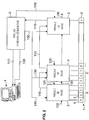
- the device according to the invention represented on the figure 2 , comprises a probe 1, basic modules 2, a synchro-sequencer module 3 and data processing means 4.
- the processing means 4 advantageously consist of a microcomputer.
- Each probe element 5 makes it possible to emit an ultrasonic signal in a material and to detect, in return, the signal refracted by this material.
- each probe element 5 is of the piezo-composite type.
- a base module 2 communicates with the following basic module 2 via a summing bus 100 of the five deviations managed by each base module 2.
- the data collected by each basic module 2 is transferred to the next basic module 2 via a data bus 110 consisting of a high-speed serial line.
- the last basic module 2 transfers all the data obtained to the data processing means 4, via the synchro-sequencer module 3, also via a data bus 110, consisting of a high-speed serial line. debit.
- the data processing means 4 communicate with each basic module 2, via the synchro-sequencer module 3, via an adjustment and configuration bus 130.
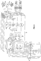
- a basic module 2 is shown in more detail on the figure 3 .
- Each basic module 2 comprises transmitting and receiving means 7, delay circuits 8, a processor 9 and a transfer multiplexer 10.
- Each basic module 2 comprises four times transmission and reception means 7, that is to say once per probe element 5.
- Each base module 2 has five times delay circuits 8, that is to say once per deflection.
- the transmission and reception means 7 comprise, for transmission, a transmitter memory 11, a digital-analog converter 12, an analog low-low filter 13 and an amplifier 14.
- the transmitting and receiving means 7 also comprise, for each probe element 5, for reception, a clipper 15, an analog filter 16, an analog digital converter 17 and a first digital interpolator 18 with parallel outputs.
- Each basic module 2 has the function of managing the four probe elements 5 of a group 6, as well as the emission of a composite wave corresponding to five different deviations I to V emitted by each probe element 5 of a group 6.
- emission curves are calculated during the initialization phase of the device according to the invention, with an accuracy ten times greater than the desired resolution.
- Each curve consists of the sum, according to emission delay laws, of the curves required for each of the five predetermined deviations of the ultrasonic beam emitted by a given group 6.
- the figure 4 illustrates, for three deviations (0 and plus or minus 45 degrees) the shape of the delay law, that is to say the amplitude of the signal emitted by each probe element 5 as a function of time.
- These curves also take into account the emission apodization coefficients intended to reduce the secondary lobes due to the spatial sampling of the probe 1.
- the precision of the calculation of the curves must be 0.5 nano-seconds.
- the sampling frequency H can, in turn, be limited to about three times the frequency of the probe 1, or 60MHz. This is sufficient for a correct reconstruction of the signal and has the advantage of limiting the material resources and therefore the cost of the device according to the invention. Working with the lowest possible H system frequency results in large delays with minimal hardware resources.
- each transmitter memory 11 is read at the sampling frequency H.
- the digital data corresponding to the recorded emission curves in each transmitter memory 11 of a channel corresponding to a given sensor element 5 are converted, also at the sampling frequency H, after their playback, into analog signals by the digital-to-analog converter 12 of the same channel.
- the analog signal obtained is then filtered by the corresponding analog low-low filter 13, so as to reject the high frequency components due to the sampling.
- the filtered signal is then amplified by the corresponding amplifier 14.
- This amplifier 14 is a linear power amplifier for supplying the energy required for the excitation of a probe element 5.
- the signals emitted by the different probe elements 5 in the material are refracted by the latter. These refracted signals are collected by each element of probe 5.
- the limiter 15 protects the circuit elements 16, 17, 18 at the input of the signals collected.
- the analog filter 16 filters the signals to let only the frequency components of the useful band. Finally, they are converted, at the frequency H / n, by the analog-digital converter 17, with a minimum dynamic of 14 bits. This makes it possible to obtain sufficient input dynamics to avoid any analog gain control at the input, as well as any saturation phenomenon. This dynamic is also sufficient to deal with any of the deviations.
- the first interpolator 18 performs, on the output signal of the digital analog converter 17, a digital filter interpolation, so as to obtain the temporal resolution necessary for the accuracy of the desired delay to perform the various deviations considered.
- the system frequency H is, as we have seen previously, equal to about three times the frequency of the probe 1. This would not be sufficient to obtain the necessary resolution on the first delay cells 19 constituting the circuits. delay 8 and located downstream of the analog-digital converter 17, because this resolution is set at one-tenth of the wavelength.
- the first interpolator 18 makes it possible to solve this problem by multiplying by four the temporal resolution, without increasing the system frequency H.
- the resolution of the delay circuits of the delay circuits 8 is of the order of four nano-seconds.
- the delay circuits 8 comprise, for each deviation I to V, a first delay cell 19, a first summer 20, a second delay cell 21, a second adder 22, and a multiplier circuit 23 and processing modules for operation 24, 24a.
- the first delay cell 19 manages the delays in a group 6 of four probe elements 5.
- Each first delay cell 19 consists of a multiplexer 25, a first circular buffer circuit 26 and a first divider circuit 26a.
- the multiplexer 25 selects the signals from the transmitting and receiving means 7 for each probe element 5 with the resolution of the tenth of a wavelength.
- the circular buffer circuit 26 applies a delay to each selected signal.
- the circular buffer circuit 26 makes it possible to obtain delays of several wavelengths while working at the frequency H / n.
- the first divider circuit 26a performs a reception apodization which reduces the sidelobes due to the spatial sampling of the probe 1.
- the first delay cell 19 is dynamically driven on writing by a first memory circuit 27 and a second interpolator 28.
- the first memory circuit 27 stores, in the initialization phase, the characteristic points of the delay curve of the element of corresponding probe 5.
- the second interpolator 28 regenerates the intermediate points at these characteristic points.
- the first delay cell 19 has a resolution of the order of one-tenth of the wavelength.
- the first summator 20 adds the signals from the first delay cells 19 of each probe element 5 of a group 6 after they have been phased by the delays applied thereto by the delay cells 19.
- Each second delay cell 21 comprises a second circular buffer circuit 29. Each second delay cell 21 manages the delays between the groups 6. These delays can reach several hundred wavelengths. Each delay cell 21 is dynamically driven on writing by a second memory circuit 30 and a third interpolator 31.
- the second memory circuit 30 stores, during the initialization phase of the device according to the invention, the characteristic points of the curve. Each third interpolator 31 regenerates the intermediate points at the characteristic points.
- the second delay cell 21 functions, like the first delay cell 19, at the frequency H / n.
- the second delay cell 21a has a resolution of one third of the wavelength.
- the second adder 22 adds the signals of a group 6, with the signals from the previous group.
- serial link The data transmission for summation, by the second summator 22, between groups 6, is performed by high speed serial link through a serializer 32 and a deserializer 32a.
- serial links can convey speeds of the order of 1.5 Gb / s.
- deserializers are of the LVDS type (LVDS is the acronym for the English expression “Low Voltage Differential Signaling” which translates to "low voltage differential signaling”). These arrangements make it possible to keep all the bits added by the first 20 and second summers and thus to have a perfectly linear processing chain, with an output dynamic range of between 96 dB and 132 dB, for a probe 1 of 8 to 2043 elements. probe 5.
- the signal resulting from the summation by the second adder 22 is applied to a gain by the multiplier circuit 23.
- the multiplier circuit 23 is dynamically driven by a third memory circuit 33 and a fourth interpolator 34.
- the third memory circuit 33 stores the characteristic points of a gain curve. This gain curve has been stored in the third memory circuit 33 during the initialization phase.
- the fourth interpolator 34 generates the intermediate points between the characteristic points of the gain curve stored in the third memory circuit 33.
- a fifth digital interpolator makes it possible to recover the temporal resolution of the tenth of a wavelength without increasing the system frequency H. This resolution is sufficient to allow all the conventional treatments carried out by conventional control and monitoring devices. ultrasound imaging.
- the output data of the fifth interpolator 35 are processed by the processing modules for operation 24, 24a.
- These processing processing modules 24, 24a are advantageously respectively of the "echo display” (A-SCAN) and "amplitude and distance measurement in a selection window” (GATES) type.
- GATES selection window
- the signal resulting from the processing by the processing modules for operation 24, 24a is sent by the processor 9 and the transfer multiplexer 10, to the next basic module 2 or to the data processing means 4, via a serial link to broadband type LVDS.
- the device according to the invention allows the summation of signals out of phase from 0 to several hundred wavelengths, with a resolution of the order of one-tenth of a wavelength.
- each deviation can take any value in this range independently of the values of other deviations.
- the device according to the invention also authorizing the frequency coding of the signals transmitted for each deviation, the discrimination of the received signals is greatly improved.
- the range of phase shift is variable from 0 to about 10 microseconds, with a resolution of five nanoseconds.
- Delays are applied with sufficient accuracy so that over-sampling points can be dropped, so as to return to the volume and signal processing frequency, before interpolation by the first interpolator 18.
- the exemplary embodiment of the device presented above allows a fully real-time operation.
- the rate of acquisition and processing depends only on the travel time in the analyzed material, as in conventional single-channel control systems, which allows rates of several kilo-Hertz in the majority of applications.
- This device has no acquisition memory, which makes possible significant and unrestricted probing times, without any additional component cost for the analysis device.
- the device according to the invention can advantageously be associated with an overhead multiplexer which makes it possible to reduce substantially the overall cost of the analysis device.
- the use of digital delays allows angular deflections much higher than those obtained with analog circuits. Indeed, the accuracy of the digital circuits does not depend on the absolute value of the delay.
- the device according to the invention has a circular operation, that is to say that one can start and stop the transmission and the reception on any probe element 5.
- a composite wave is emitted composed of several signals emitted by all the probe elements 5 of the probe 1, with emission delay laws allowing the simultaneous emission of the wave according to several deviations.
- the delay circuits 8 then process the signals corresponding to the emitted wave, refracted by the material and collected by the probe elements 5, by applying, to these signals, reception delay laws corresponding to the different deviations.
- a composite wave is emitted composed of several signals emitted simultaneously by at least two different zones of the probe 1 each comprising several probe elements 5. Each of these zones then simultaneously scans the material at analyze, emitting the wave according to several deviations.
- the signals refracted by the material and collected by the probe elements 5, zone by zone, are then processed by applying to them reception delay laws corresponding to the different deviations of the emitted wave.
- This second example of a process is particularly advantageous.
- the scanning speed is divided by four. If, with each of the zones, the wave is transmitted according to five deviations, a factor of twenty is gained on the scanning speed of the material to be analyzed with respect to what could be obtained with the methods and devices of the prior art.
- the device and the method according to the invention apply, not exclusively, to all ultrasonic tests, namely, in the field of non-destructive testing, to portable devices and automatic systems, and in the medical field, to devices diagnosis.
- the device and method according to the invention also apply to all systems that use a sensor consisting of a plurality of independent elements, regardless of the physical phenomenon used: Foucault currents, infrasound, electromagnetic waves, etc.
- the device and method according to the invention also apply to all multi-element sensors, whether linear, matrix or circular.
Description
L'invention concerne les dispositifs d'analyse de la structure d'un matériau.The invention relates to devices for analyzing the structure of a material.
Plus précisément l'invention concerne les dispositifs d'analyse de la structure d'un matériau, selon le préambule de la revendication 1:
- une sonde comportant une pluralité d'éléments de sonde pour l'émission d'une onde, dans le matériau, avec une loi de retard d'émission correspondant à une déviation selon une direction et une focalisation de cette onde, et la réception, en parallèle sur les différents éléments de sonde, de signaux provenant de la réfraction de cette onde par le matériau,
- une pluralité d'émetteurs, chaque émetteur excitant un unique élément de sonde,
- une pluralité de voies de détection, chaque voie de détection étant connectée à un élément de sonde, pour recueillir les signaux de réfraction et les transmettre à des moyens de traitement de données,
- une pluralité de circuits de retard, chaque circuit de retard appliquant un retard, sur chaque voie de détection, selon une loi de retard de réception prédéterminée correspondant à la déviation de l'onde émise.
- a probe comprising a plurality of probe elements for transmitting a wave in the material, with a transmission delay law corresponding to a deflection in one direction and a focusing of this wave, and the reception, in parallel on the different probe elements, signals coming from the refraction of this wave by the material,
- a plurality of emitters, each emitter exciting a single probe element,
- a plurality of detection channels, each detection channel being connected to a probe element, for collecting the refraction signals and transmitting them to data processing means,
- a plurality of delay circuits, each delay circuit applying a delay, on each detection channel, according to a predetermined reception delay law corresponding to the deviation of the transmitted wave.
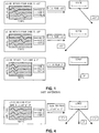
On connaît déjà de tels dispositifs d'analyse. Ils sont couramment utilisés de manière séquentielle, comme illustré par la
L'analyse s'effectue alors en réalisant un tir, c'est-à-dire l'émission d'une onde par l'ensemble des éléments de sonde selon une déviation donnée, pour chaque déviation d'exploration souhaitée. Chaque déviation correspond à une loi de retard distincte. Le matériau est exploré ligne par ligne au moyen d'un faisceau mobile, la ligne d'exploration étant déplacée entre chaque tir.The analysis is then performed by performing a firing, that is to say the emission of a wave by the set of probe elements according to a given deflection, for each desired exploration deviation. Each deviation corresponds to a separate law of delay. The material is explored line by line by means of a moving beam, the line of exploration being moved between each shot.
Dans ces conditions, le temps nécessaire à la constitution d'une image croit avec la résolution spatiale exigée, avec le temps de parcours de l'onde dans l'objet analysé et avec la résolution de l'image reconstituée. Les dispositifs d'analyse de ce type ne permettent pas en pratique de dépasser quelques centaines de Hertz de cadence d'images, ce qui est très insuffisant dans de nombreuses applications telles que le contrôle de tôles, de tubes, de rails en voie, etc.Under these conditions, the time required for the constitution of an image increases with the required spatial resolution, with the travel time of the wave in the analyzed object and with the resolution of the reconstituted image. The analysis devices of this type do not allow in practice to exceed a few hundreds of Hertz frame rate, which is very insufficient in many applications such as control of sheets, tubes, rails track, etc. .
Un but de l'invention est de pallier cet inconvénient.An object of the invention is to overcome this drawback.
Ce but est atteint, selon l'invention, par un dispositif d'analyse selon la revendication 1, dans lequel chaque élément de sonde émet l'onde avec au moins une autre loi de retard d'émission correspondant à l'émission de l'onde selon au moins une autre déviation, simultanément, et les circuits de retard appliquent des retards, sur chaque voie de détection, selon au moins une autre loi de retard de réception, prédéterminée et correspondant à la réception de l'onde émise selon l'autre déviation. En effet, les lois de retard d'émission et de réception utilisées dans le dispositif selon l'invention correspondent à une pluralité de déviations qui auraient, avec les dispositifs de l'art antérieur, nécessité autant de tirs que de déviations, alors que le dispositif de l'invention analyse le matériau selon différentes déviations, en simultané, en un seul tir.This object is achieved, according to the invention, by an analysis device according to
Dans des modes de réalisation préférés du dispositif selon l'invention, on a recours à l'une et/ou à l'autre des dispositions suivantes :
- il comporte des moyens de pilotage des circuits de retard aptes à piloter les circuits de retard pour traiter chaque onde selon une focalisation variant en fonction du temps ;
- il comporte des moyens de numérisation du signal recueilli par chacune des voies de détection, avec une fréquence d'échantillonnage comprise entre deux et cinq fois la fréquence d'émission des éléments de sonde, et préférentiellement sensiblement égale à trois fois la fréquence d'émission des éléments de sonde ;
- il comporte un interpolateur numérique à sorties parallèles pour multiplier la résolution temporelle du signal recueilli par chacune des voies de détection ;
- il comporte un amplificateur linéaire pour amplifier l'amplitude de l'onde avant son émission par les éléments de sonde ; et
- les éléments de sonde sont agencés selon une disposition choisie parmi une disposition linéaire, une disposition matricielle et une disposition circulaire. Un procédé d'analyse de la structure d'un matériau comprenant :
- l'émission d'une onde composite constituée d'une pluralité de signaux émis par une sonde comportant une pluralité d'éléments de sonde, avec une loi de retard d'émission correspondant à une déviation selon une direction et une focalisation de cette onde,
- la réception, en parallèle, par les éléments de sonde, de signaux provenant de la réfraction de l'onde, par le matériau,
- la transmission, par une pluralité de voies de détection, des signaux reçus par les éléments de sonde, vers des moyens de traitement de données,
- l'application d'un retard par des circuits de retard, en parallèle sur chaque voie de détection, selon une loi de retard de réception, prédéterminée et correspondant à la déviation de l'onde émise, le procédé comporte en outre l'émission d'au moins une autre onde, selon une autre déviation, correspondant à une autre loi de retard, l'émission de chaque onde étant effectuée de manière simultanée, et par le fait que la loi de retard correspond à l'émission simultanée des différentes ondes, respectivement selon chacune des déviations.
- it comprises means for controlling the delay circuits capable of driving the delay circuits in order to process each wave according to a time-varying focusing;
- it comprises means for digitizing the signal collected by each of the detection channels, with a sampling frequency of between two and five times the transmission frequency of the probe elements, and preferably substantially equal to three times the transmission frequency probe elements;
- it comprises a digital interpolator with parallel outputs for multiplying the temporal resolution of the signal collected by each of the detection channels;
- it comprises a linear amplifier for amplifying the amplitude of the wave before it is emitted by the probe elements; and
- the probe elements are arranged in a disposition selected from a linear arrangement, a matrix arrangement and a circular arrangement. A method of analyzing the structure of a material comprising:
- the emission of a composite wave consisting of a plurality of signals emitted by a probe comprising a plurality of probe elements, with a transmission delay law corresponding to a deflection in one direction and a focusing of this wave,
- the reception, in parallel, by the probe elements, of signals originating from the refraction of the wave, by the material,
- transmitting, by a plurality of detection channels, signals received by the probe elements to data processing means,
- the application of a delay by delay circuits, in parallel on each detection channel, according to a predetermined reception delay law and corresponding to the deviation of the transmitted wave, the method furthermore comprises the emission of at least one other wave, according to another deviation, corresponding to another law of delay, the emission of each wave being effected simultaneously, and in that the law of delay corresponds to the simultaneous emission of the different waves , respectively according to each of the deviations.
Dans des modes de mise en oeuvre préférés du procédé on a recours à l'une et/ou à l'autre des dispositions suivantes :
- il comporte une numérisation des signaux transmis par chaque voie de réception, avec une fréquence d'échantillonnage comprise entre deux et cinq fois la fréquence d'émission des éléments de sonde, et préférentiellement sensiblement égale à trois fois la fréquence d'émission des éléments de sonde ; et
- il comporte successivement les étapes selon lesquelles :
- un premier retard est appliqué à chaque signal correspondant à une voie de détection,
- plusieurs signaux correspondant à un groupe d'éléments de sonde sont sommés,
- un deuxième retard est appliqué pour chaque groupe, à chaque signal résultant de la sommation précédente, et
- les signaux retardés correspondant aux différents groupes sont sommés ;
- au moins deux zones différentes de la sonde, comportant chacune une pluralité d'éléments de sonde, balayent simultanément le matériau, selon toutes les déviations également simultanément ;
- les signaux reçus par les différents élément de sonde sont traités, à mesure de leur réception, en continu, par les circuits de retard ; et
- les signaux reçus par les différents élément de sonde sont mémorisés pour être traités en différé par les circuits de retard.
- it comprises a digitization of the signals transmitted by each reception channel, with a sampling frequency of between two and five times the transmission frequency of the probe elements, and preferably substantially equal to three times the transmission frequency of the elements of the probe. probe; and
- it comprises successively the steps according to which:
- a first delay is applied to each signal corresponding to a detection channel,
- several signals corresponding to a group of probe elements are summed,
- a second delay is applied for each group, to each signal resulting from the previous summation, and
- the delayed signals corresponding to the different groups are summed;
- at least two different areas of the probe, each having a plurality of probe elements, simultaneously scan the material, in all deviations also simultaneously;
- the signals received by the different probe elements are processed, as they are received, continuously by the delay circuits; and
- the signals received by the different probe elements are stored in order to be processed later by the delay circuits.
D'autres aspects, buts et avantages de l'invention apparaîtront à la lecture de la description détaillée qui suit d'un de ses modes de réalisation.Other aspects, objects and advantages of the invention will appear on reading the detailed description which follows of one of its embodiments.
L'invention sera également mieux comprise à l'aide des références aux dessins sur lesquels :
- la
figure 1 représente schématiquement les différentes étapes mises en oeuvre, avec un procédé de l'art antérieur, pour obtenir une analyse d'un matériau, selon trois déviations différentes ; - la
figure 2 est un synoptique général d'un mode de réalisation du dispositif selon l'invention ; - la
figure 3 est un synoptique d'un module de base du mode de réalisation du dispositif selon l'invention représenté sur lafigure 2 ; et - la
figure 4 illustre schématiquement la correspondance entre lois de retard et déviations de l'onde émise par le dispositif correspondant auxfigures 2 et 3 .
- the
figure 1 schematically represents the different steps implemented, with a method of the prior art, to obtain an analysis of a material, according to three different deviations; - the
figure 2 is a general block diagram of an embodiment of the device according to the invention; - the
figure 3 is a block diagram of a basic module of the embodiment of the device according to the invention shown in FIG.figure 2 ; and - the
figure 4 schematically illustrates the correspondence between the laws of delay and deviations of the wave emitted by the device corresponding to thefigures 2 and3 .
Un exemple de mode de réalisation du dispositif selon l'invention est présenté ci-dessous.An exemplary embodiment of the device according to the invention is presented below.
Selon cet exemple, le dispositif selon l'invention, représenté sur la
La sonde 1 est constituée de n éléments de sonde 5. Ce nombre n est fonction de l'application souhaitée et/ou des limites technologiques de fabrication. A titre d'exemple, n = 128. Ces n éléments de sonde 5 sont répartis par groupe 6 de quatre éléments de sonde 5 consécutifs, répartis sur la sonde 1. Chaque groupe 6 est traité par un module de base 2.The
Chaque élément de sonde 5 permet d'émettre un signal ultrasonore dans un matériau et de détecter, en retour, le signal réfracté par ce matériau. Avantageusement, chaque élément de sonde 5 est du type piézo-composite.Each
Un module de base 2 communique avec le module de base 2 suivant par l'intermédiaire d'un bus de sommation 100 des cinq déviations gérées par chaque module de base 2.A
Les données recueillies par chaque module de base 2 sont transférées au module de base 2 suivant par l'intermédiaire d'un bus de données 110 constitué d'une ligne série à haut débit. Le dernier module de base 2 transfère l'ensemble des données obtenues aux moyens de traitement de données 4, via le module synchro-séquenceur 3, également par l'intermédiaire d'un bus de données 110, constitué d'une ligne série à haut débit.The data collected by each
Le module synchro-séquenceur 3 a pour principale fonction d'interfacer les modules de base 2 et les moyens de traitement 4 et de générer des signaux de synchronisation à partir d'horloges internes ou externes, pour les transmettre aux modules de base 2 par l'intermédiaire d'un bus de synchronisation 120. En particulier, l'interfaçage entre les modules de base 2 et les moyens de traitement 4 comporte :
- le stockage des données détectées, dans une mémoire tampon, via un désérialiseur qui récupère ces données, provenant des modules de
base 2, sur le bus de données 110 ; - la gestion des transferts de ces données vers les moyens de traitement 4 via des interfaces appropriées ; et
- le paramétrage des différents modules de
base 2, à partir des données en provenance des moyens de traitement de données 4.
- storing the detected data in a buffer via a deserializer which retrieves this data from the
base modules 2 on thedata bus 110; - managing the transfer of these data to the processing means 4 via appropriate interfaces; and
- the parameterization of the different
basic modules 2, from the data coming from the data processing means 4.
Les moyens de traitement de données 4 communiquent avec chaque module de base 2, via le module synchro-séquenceur 3, par l'intermédiaire d'un bus de réglage et de configuration 130.The data processing means 4 communicate with each
Un module de base 2 est représenté de manière plus détaillée sur la
Chaque module de base 2 comporte quatre fois des moyens d'émission et de réception 7, c'est-à-dire une fois par élément de sonde 5.Each
Chaque module de base 2 comporte cinq fois des circuits de retard 8, c'est-à-dire une fois par déviation.Each
Pour chaque élément de sonde 5, les moyens d'émission et de réception 7 comprennent, pour l'émission, une mémoire émetteur 11, un convertisseur digital-analogique 12, un filtre basse-bas analogique 13 et un amplificateur 14.For each
Les moyens d'émission et de réception 7 comportent également, pour chaque élément de sonde 5, pour la réception, un écrêteur 15, un filtre analogique 16, un convertisseur analogique numérique 17 et un premier interpolateur 18 numérique à sorties parallèles.The transmitting and receiving means 7 also comprise, for each
Chaque module de base 2 a pour fonction de gérer les quatre éléments de sonde 5 d'un groupe 6, ainsi que l'émission d'une onde composée correspondant à cinq déviations I à V différentes émises par chaque élément de sonde 5 d'un groupe 6.Each
La gestion, par chaque module de base 2, des éléments de sonde 5 comporte, en particulier :
- l'émission d'ultrasons,
- la détection de signaux ultrasonores,
- la conversion analogique/numérique des signaux détectés, et
- l'interpolation numérique des signaux détectés, de manière à accroître la résolution temporelle.
- the emission of ultrasound,
- the detection of ultrasonic signals,
- the analog / digital conversion of the detected signals, and
- the digital interpolation of the detected signals, so as to increase the temporal resolution.
Pour l'émission, des courbes d'émission sont calculées en phase d'initialisation du dispositif selon l'invention, avec une précision dix fois supérieure à la résolution souhaitée. Chaque courbe est constituée de la somme, selon des lois de retard d'émission, des courbes nécessaires pour chacune des cinq déviations prédéterminées du faisceau ultrasonore émis par un groupe 6 donné. La
Ces courbes d'émission sont échantillonnées à une fréquence système H. Les courbes échantillonnées correspondantes sont alors chargées dans chaque mémoire émetteur 11.These emission curves are sampled at a system frequency H. The corresponding sampled curves are then loaded into each
Ainsi, par exemple, pour une sonde de 20MHz, la précision du calcul des courbes doit être de 0,5 nano-secondes. La fréquence d'échantillonnage H peut, quant à elle, être limitée à environ trois fois la fréquence de la sonde 1, soit 60MHz. Ceci est suffisant pour une reconstruction correcte du signal et présente l'avantage de limiter les ressources matérielles et donc le coût du dispositif selon l'invention. Le fait de travailler avec une fréquence système H la plus basse possible permet d'obtenir de grands retards avec un minimum de ressources matérielles.Thus, for example, for a probe of 20 MHz, the precision of the calculation of the curves must be 0.5 nano-seconds. The sampling frequency H can, in turn, be limited to about three times the frequency of the
En phase de tir, c'est-à-dire en phase d'émission de l'onde par la sonde 1, chaque mémoire émetteur 11 est relue à la fréquence d'échantillonnage H. Les données numériques correspondantes aux courbes d'émission enregistrées dans chaque mémoire émetteur 11 d'une voie correspondant à un élément de sonde 5 donné, sont converties, également à la fréquence d'échantillonnage H, après leur relecture, en signaux analogiques par le convertisseur digital-analogique 12 de la même voie. Le signal analogique obtenu est alors filtré par le filtre basse-bas analogique 13 correspondant, de manière à rejeter les composantes haute fréquence dues à l'échantillonnage. Le signal filtré est ensuite amplifié par l'amplificateur 14 correspondant. Cet amplificateur 14 est un amplificateur linéaire de puissance permettant de fournir l'énergie nécessaire à l'excitation d'un élément de sonde 5.In the firing phase, that is to say in the transmission phase of the wave by the
Les signaux émis par les différents éléments de sonde 5 dans le matériau sont réfractés par celui-ci. Ces signaux réfractés sont recueillis par chaque élément de sonde 5. L'écrêteur 15 protège les éléments de circuit 16, 17, 18 en entrée des signaux recueillis. Puis le filtre analogique 16 filtre les signaux afin de ne laisser passer que les composantes fréquentielles de la bande utile. Enfin, ils sont convertis, à la fréquence H/n, par le convertisseur analogique-numérique 17, avec une dynamique minimum de 14 bits. Ceci permet d'obtenir une dynamique d'entrée suffisante pour éviter toute commande de gain analogique à l'entrée, ainsi que tout phénomène de saturation. Cette dynamique est également suffisante pour traiter n'importe laquelle des déviations.The signals emitted by the
Le premier interpolateur 18 effectue, sur le signal en sortie du convertisseur analogique numérique 17, une interpolation par filtrage numérique, de façon à obtenir la résolution temporelle nécessaire à la précision du retard souhaité pour effectuer les différentes déviations envisagées. En effet, la fréquence système H est, comme nous l'avons vu précédemment, égale à environ trois fois la fréquence de la sonde 1. Ce qui ne serait pas suffisant pour obtenir la résolution nécessaire sur des premières cellules de retard 19 constitutives des circuits de retard 8 et situées en aval du convertisseur analogique-digital 17, car cette résolution est fixée au dixième de la longueur d'onde. Mais le premier interpolateur 18 permet de résoudre ce problème en multipliant par quatre la résolution temporelle, sans augmenter la fréquence système H. Ainsi, pour une sonde de 20MHz et une fréquence système de 60MHz, la résolution des circuits de retard des circuits de retard 8 est de l'ordre de quatre nano-secondes.The first interpolator 18 performs, on the output signal of the digital analog converter 17, a digital filter interpolation, so as to obtain the temporal resolution necessary for the accuracy of the desired delay to perform the various deviations considered. Indeed, the system frequency H is, as we have seen previously, equal to about three times the frequency of the
Les circuits de retard 8 comprennent, pour chaque déviation I à V, une première cellule de retard 19, un premier sommateur 20, une deuxième cellule de retard 21, un deuxième sommateur 22, ainsi qu'un circuit multiplieur 23 et des modules de traitement pour exploitation 24, 24a.The
Les circuits de retard 8 gèrent, en particulier:
- l'application, en parallèle sur l'ensemble des signaux détectés, des retards selon des lois de retard de réception correspondant aux différentes déviations souhaitées,
- des pondérations par des coefficients d'apodisation,
- la sommation numérique en temps réel des différents signaux retardés et pondérés, afin de générer les signaux correspondant aux différentes déviations souhaitées ; et
- l'application d'un gain aux signaux retardés, pondérés et sommés.
- applying, in parallel to all the detected signals, delays according to reception delay laws corresponding to the different desired deviations,
- weightings by apodization coefficients,
- the real-time numerical summation of the different delayed and weighted signals, in order to generate the signals corresponding to the different desired deviations; and
- applying a gain to delayed, weighted and summed signals.
En sortie du premier interpolateur 18, pour chaque élément de sonde 5 et pour chacun des circuits de retard 8, la première cellule de retard 19 gère les retards dans un groupe 6 de quatre éléments de sonde 5.At the output of the first interpolator 18, for each
Chaque première cellule de retard 19 est constituée d'un multiplexeur 25, d'un premier circuit tampon circulaire 26 et d'un premier circuit diviseur 26a. Le multiplexeur 25 sélectionne les signaux issus des moyens d'émission et de réception 7 pour chaque élément de sonde 5 avec la résolution du dixième de longueur d'onde. Le circuit tampon circulaire 26 applique un retard à chaque signal sélectionné. Le circuit tampon circulaire 26 permet d'obtenir des retards de plusieurs longueurs d'onde en travaillant à la fréquence H/n. Le premier circuit diviseur 26a réalise une une apodisation en réception qui réduit les lobes secondaires dus à l'échantillonnage spatial de la sonde 1.Each
La première cellule de retard 19 est pilotée dynamiquement à l'écriture par un premier circuit mémoire 27 et un deuxième interpolateur 28. Le premier circuit mémoire 27 stocke, en phase d'initialisation, les points caractéristiques de la courbe de retard de l'élément de sonde 5 correspondant. Le deuxième interpolateur 28 régénère les points intermédiaires à ces points caractéristiques.The
La première cellule de retard 19 a une résolution de l'ordre du dixième de la longueur d'onde.The
Le premier sommateur 20 additionne les signaux issus des premières cellules de retard 19 de chaque élément de sonde 5 d'un groupe 6, après qu'ils aient été mis en phase par les retards appliqués à ceux-ci par les cellules de retard 19.The
Chaque deuxième cellule de retard 21 comprend un deuxième circuit tampon circulaire 29. Chaque deuxième cellule de retard 21 gère les retards entre les groupes 6. Ces retards peuvent atteindre plusieurs centaines de longueurs d'onde. Chaque cellule de retard 21 est pilotée dynamiquement à l'écriture par un deuxième circuit mémoire 30 et un troisième interpolateur 31. Le deuxième circuit mémoire 30 stocke, pendant la phase d'initialisation du dispositif selon l'invention, les points caractéristiques de la courbe de retard de chaque groupe 6. Le troisième interpolateur 31 régénère les points intermédiaires aux points caractéristiques. La deuxième cellule de retard 21 fonctionne, comme la première cellule de retard 19, à la fréquence H/n.Each
La deuxième cellule de retard 21a une résolution de l'ordre du tiers de la longueur d'onde.The second delay cell 21a has a resolution of one third of the wavelength.
Le deuxième sommateur 22 additionne les signaux d'un groupe 6, avec les signaux provenant du groupe précédent.The
La transmission des données pour sommation, par le deuxième sommateur 22, entre groupes 6, est effectuée par liaison série à haut débit au travers d'un sérialiseur 32 et d'un désérialiseur 32a. Avantageusement, ces liaisons série permettent d'acheminer des débits de l'ordre de 1,5Go/s. Avantageusement également, les désérialiseurs sont de type LVDS (LVDS est l'acronyme de l'expression anglo-saxonne « Low Voltage Differential Signaling » qui se traduit par « signalisation différentielle à basse tension »). Ces dispositions permettent de conserver tous les bits ajoutés par les premier 20 et deuxième 22 sommateurs et d'avoir ainsi une chaîne de traitement parfaitement linéaire, avec une dynamique de sortie comprise entre 96dB et 132dB, pour une sonde 1 de 8 à 2043 éléments de sonde 5.The data transmission for summation, by the
Le signal issu de la sommation par le deuxième sommateur 22 se voit appliquer un gain par le circuit multiplieur 23. Le circuit multiplieur 23 est piloté dynamiquement par un troisième circuit mémoire 33 et un quatrième interpolateur 34. Le troisième circuit mémoire 33 stocke les points caractéristiques d'une courbe de gain. Cette courbe de gain a été stockée dans le troisième circuit mémoire 33 pendant la phase d'initialisation. Le quatrième interpolateur 34 génère les points intermédiaires entre les points caractéristiques de la courbe de gain stockés dans le troisième circuit mémoire 33.The signal resulting from the summation by the
Un cinquième interpolateur 35 numérique, à sortie parallèle, permet de retrouver la résolution temporelle du dixième de longueur d'onde sans augmenter la fréquence système H. Cette résolution est suffisante pour autoriser tous les traitements conventionnels effectués par des appareils classiques de contrôle et d'imagerie par ultrasons. Les données en sortie du cinquième interpolateur 35 sont traitées par les modules de traitement pour exploitation 24, 24a. Ces modules de traitement pour exploitation 24, 24a sont avantageusement respectivement du type "affichage des échos" (A-SCAN) et "mesures d'amplitudes et de distances dans une fenêtre de sélection" (GATES). Ces modules de traitement pour exploitation 24, 24a sont tout à fait conventionnels dans le domaine du contrôle non destructif et de l'imagerie par ultrasons.A fifth digital interpolator, with parallel output, makes it possible to recover the temporal resolution of the tenth of a wavelength without increasing the system frequency H. This resolution is sufficient to allow all the conventional treatments carried out by conventional control and monitoring devices. ultrasound imaging. The output data of the
Le signal résultant du traitement par les modules de traitement pour exploitation 24, 24a est envoyé par le processeur 9 et le multiplexeur de transfert 10, vers le module de base 2 suivant ou vers les moyens de traitement de données 4, via une liaison série à haut débit de type LVDS.The signal resulting from the processing by the processing modules for
Dans l'exemple de dispositif selon l'invention décrit ci-dessus, les lois de retard de réception sont appliquées, d'une part, au niveau des premières cellules de retard 19 et, d'autre part, au niveau des deuxièmes cellules de retard 21. Ceci permet d'avoir :
- des premières cellules de retard 19 pouvant appliquer des retards égaux à, par exemple, quarante fois la longueur de l'onde émise dans le matériau, avec une relativement bonne résolution (par exemple de l'ordre du dixième de longueur d'onde) ; et
- des deuxièmes cellules de retard 21 pouvant appliquer des retards égaux à, par exemple, cent soixante fois la longueur de l'onde émise dans le matériau, avec une relativement faible résolution (par exemple de l'ordre du tiers de longueur d'onde).
-
first delay cells 19 which can apply delays equal to, for example, forty times the length of the wave emitted in the material, with a relatively good resolution (for example of the order of one-tenth of a wavelength); and -
second delay cells 21 which can apply delays equal to, for example, one hundred and sixty times the length of the wave emitted in the material, with a relatively low resolution (for example of the order of one-third of a wavelength) .
Le dispositif selon l'invention permet la sommation de signaux déphasés de 0 à plusieurs centaines de longueurs d'onde, avec une résolution de l'ordre du dixième de longueur d'onde. On obtient, grâce au dispositif selon l'invention, des déviations du faisceau ultrasonore émis par la sonde 1 de 0 degré à plus ou moins 90 degrés, chaque déviation pouvant prendre n'importe quelle valeur dans cette plage indépendamment des valeurs des autres déviations. Le dispositif selon l'invention autorisant par ailleurs le codage fréquentiel des signaux émis pour chaque déviation, la discrimination des signaux reçus s'en trouve grandement améliorée.The device according to the invention allows the summation of signals out of phase from 0 to several hundred wavelengths, with a resolution of the order of one-tenth of a wavelength. We obtain, thanks to the device according to the invention, deviations of the ultrasonic beam emitted by the
A titre d'exemple, pour une sonde de 20MHz et donc une période de 50 nano-secondes, la gamme de déphasage est variable de 0 à environ 10 microsecondes, avec une résolution de cinq nano-secondes.For example, for a probe of 20 MHz and therefore a period of 50 nanoseconds, the range of phase shift is variable from 0 to about 10 microseconds, with a resolution of five nanoseconds.
Les retards sont appliqués avec une précision suffisante pour que des points de sur-échantillonnage puissent être abandonnés, de façon à revenir au volume et à la fréquence de traitement des signaux, avant interpolation par le premier interpolateur 18.Delays are applied with sufficient accuracy so that over-sampling points can be dropped, so as to return to the volume and signal processing frequency, before interpolation by the first interpolator 18.
L'exemple de mode de réalisation du dispositif présenté ci-dessus permet un fonctionnement totalement en temps réel. La cadence d'acquisition et de traitement ne dépend que du temps de parcours dans le matériau analysé, comme dans les systèmes de contrôle mono-voie classiques, ce qui autorise des cadences de plusieurs kilo-Hertz dans la majorité des applications. Ce dispositif ne comporte pas de mémoire d'acquisition, ce qui rend possible des durées de sondage importantes et non limitées, sans aucun surcoût de composants pour le dispositif d'analyse. Lorsque les conditions de contrôle ne nécessitent pas des cadences de plusieurs kilo-Hertz, le dispositif selon l'invention peut avantageusement être associé à un multiplexeur en tête qui permet de réduire sensiblement le coût global du dispositif d'analyse. Par ailleurs, l'utilisation de circuits de retards numériques, permet des déflexions angulaires nettement supérieures à celles obtenues avec les circuits analogiques. En effet, la précision des circuits numériques ne dépend pas de la valeur absolue du retard.The exemplary embodiment of the device presented above allows a fully real-time operation. The rate of acquisition and processing depends only on the travel time in the analyzed material, as in conventional single-channel control systems, which allows rates of several kilo-Hertz in the majority of applications. This device has no acquisition memory, which makes possible significant and unrestricted probing times, without any additional component cost for the analysis device. When the control conditions do not require rates of several kilo-Hertz, the device according to the invention can advantageously be associated with an overhead multiplexer which makes it possible to reduce substantially the overall cost of the analysis device. Moreover, the use of digital delays, allows angular deflections much higher than those obtained with analog circuits. Indeed, the accuracy of the digital circuits does not depend on the absolute value of the delay.
Le dispositif selon l'invention a un fonctionnement circulaire, c'est-à-dire que l'on peut démarrer et arrêter l'émission et la réception sur n'importe quel élément de sonde 5.The device according to the invention has a circular operation, that is to say that one can start and stop the transmission and the reception on any
Le dispositif selon l'invention, décrit ci-dessus permet la mise en oeuvre de plusieurs procédés également conformes à la présente invention.The device according to the invention, described above, allows the implementation of several methods also in accordance with the present invention.
Selon un premier exemple de procédé selon l'invention, on émet une onde composite constituée de plusieurs signaux émis par l'ensemble des éléments de sonde 5 de la sonde 1, avec des lois de retard d'émission permettant l'émission simultanée de l'onde selon plusieurs déviations. Les circuits de retard 8 traitent alors les signaux correspondant à l'onde émise, réfractés par le matériau et recueillis par les éléments de sonde 5, en appliquant, à ces signaux, des lois de retard de réception correspondant aux différentes déviations.According to a first exemplary method according to the invention, a composite wave is emitted composed of several signals emitted by all the
Selon un deuxième exemple de procédé selon l'invention, on émet une onde composite constituée de plusieurs signaux émis simultanément par au moins deux zones différentes de la sonde 1 comprenant chacune plusieurs éléments de sonde 5. Chacune de ces zones balaye alors simultanément le matériau à analyser, en émettant l'onde selon plusieurs déviations. On traite alors les signaux réfractés par le matériau et recueillis par les éléments de sonde 5, zone par zone, en leur appliquant des lois de retard de réception correspondant aux différentes déviations de l'onde émise.According to a second example of a method according to the invention, a composite wave is emitted composed of several signals emitted simultaneously by at least two different zones of the
Ce deuxième exemple de procédé est particulièrement avantageux. En effet, par exemple en divisant la surface du matériau à analyser en quatre plages et en analysant chacune de ces plages avec une zone différente de la sonde 1, on divise par quatre la vitesse de balayage. Si on émet, avec chacune des zones, l'onde selon cinq déviations, on gagne un facteur vingt sur la vitesse de balayage du matériau à analyser par rapport à ce qui pouvait être obtenu avec les procédés et dispositifs de l'art antérieur.This second example of a process is particularly advantageous. In fact, for example by dividing the surface of the material to be analyzed into four ranges and by analyzing each of these areas with a different zone of the
Le dispositif et le procédé selon l'invention s'appliquent, non exclusivement, à tous les contrôles par ultrasons, à savoir, dans le domaine du contrôle non destructif, aux appareils portatifs et aux systèmes automatiques, et dans le domaine médical, aux appareils de diagnostic.The device and the method according to the invention apply, not exclusively, to all ultrasonic tests, namely, in the field of non-destructive testing, to portable devices and automatic systems, and in the medical field, to devices diagnosis.
Le dispositif et le procédé selon l'invention s'appliquent également à tous les systèmes qui utilisent un capteur constitué d'une pluralité d'éléments indépendants, quel que soit le phénomène physique exploité : Courants de Foucault, infrasons, ondes électromagnétiques, etc.The device and method according to the invention also apply to all systems that use a sensor consisting of a plurality of independent elements, regardless of the physical phenomenon used: Foucault currents, infrasound, electromagnetic waves, etc.
Le dispositif et le procédé selon l'invention s'appliquent également à tous les capteurs multi-éléments, qu'ils soient linéaires, matriciels ou circulaires.The device and method according to the invention also apply to all multi-element sensors, whether linear, matrix or circular.
De nombreuses variantes du dispositif et du procédé selon l'invention peuvent être prévues aux modes de réalisation et de mise en oeuvre décrits ci-dessus, sans sortir du cadre de l'invention.Many variants of the device and method according to the invention can be provided in the embodiments and implementation described above, without departing from the scope of the invention.
Ainsi, au lieu de traiter en temps réel les signaux recueillis par les éléments de sonde 5, il est possible de prévoir une mémoire tampon en amont des circuits de retard 8, pour enregistrer ces signaux en vue d'un traitement ultérieur par ces circuits de retard 8.Thus, instead of processing in real time the signals collected by the
De même, on a décrit ci-dessus un dispositif comportant des groupes 6 de quatre éléments de sonde 5, émettant selon cinq déviations, mais les nombres de groupes 6, d'éléments de sonde 5 par groupe 6 et de déviations est variable et dépend des applications et/ou des performances des composants utilisés pour la fabrication du dispositif selon l'invention.Likewise, a
Claims (8)
- A device for analyzing the structure of a material for the nondestructive inspection of sheet metal, tubes, track rails, comprising:- a probe comprising a plurality of probe elements (5) for the emission of a wave at a wavelength, into the material, with an emission delay law corresponding to a deviation according to a direction and a focusing of this wave, and the reception, in parallel on the various probe elements (5), of signals originating from the refraction of this wave by the material,- a plurality of emitters (7), each emitter (7) exciting a single probe element (5),- a plurality of detection channels, each detection channel being connected to a probe element (5), so as to collect the refraction signals and transmit them to data processing means (4),- a plurality of delay circuits (8), each delay circuit (8) applying a delay, to each detection channel, according to a predetermined reception delay law corresponding to the deviation of the wave emitted, and wherein:• each probe element (5) emits the wave with at least one other emission delay law corresponding to the emission of the wave according to at least one other deviation, simultaneously, and that• the delay circuits apply delays to each detection channel according to at least one other predetermined reception delay law corresponding to the reception of the wave emitted according to the other deviation,characterized in that the delay circuits (8) comprise first delay cells (19) and second delay cells (21) in series and two summation circuits (20, 22) for summing the signals transmitted, after application of the delays respectively by the first (19) and second (21) delay cells, and that:- the first delay cells (19) have a first resolution,- the first summation circuits (20) adding the signals from the first delay cells (19) of a group (6) of several consecutive probe elements (5),- the second delay cells (21) have a second resolution, lower than said first resolution, and delay the signals from the first summator (20),- the second summation circuits (22) comprise a plurality of cascaded second summators, each second summator adding the signals from a second delay cell and from a previous other second summator, so as the second summator provides a signal corresponding to a deviation.
- The device as claimed in claim 1, in which the delays are comprised between zero and forty times the wavelength with a resolution of one tenth of the wavelength.
- The device as claimed in claim 1, in which the deviation and the other deviation are comprised between zero degree and plus or minus 90 degrees.
- The device as claimed in claim 1, comprising means of driving the delay circuits (8) able to drive the delay circuits (8) so as to process each wave according to a focusing varying as a function of time.
- The device as claimed in one of the preceding claims, comprising means of digitization (17) of the signal collected by each of the detection channels, with a sampling frequency lying between two and five times the frequency of emission of the probe elements (5), and preferably substantially equal to three times the frequency of emission of the probe elements (5).
- The device as claimed in one of the preceding claims, comprising a digital interpolator (18) with parallel outputs for multiplying the temporal resolution of the signal collected by each of the detection channels.
- The device as claimed in one of the preceding claims, comprising a linear amplifier for amplifying the amplitude of the wave prior to its emission by the probe elements (5).
- The device as claimed in one of the preceding claims, in which the probe elements (5) are laid out according to an arrangement chosen from among a linear arrangement, a matrix arrangement and a circular arrangement.
Applications Claiming Priority (3)
| Application Number | Priority Date | Filing Date | Title |
|---|---|---|---|
| FR0112516 | 2001-09-28 | ||
| FR0112516A FR2830328B1 (en) | 2001-09-28 | 2001-09-28 | DEVICE AND METHOD FOR ANALYZING THE STRUCTURE OF A MATERIAL |
| PCT/FR2002/003283 WO2003029808A1 (en) | 2001-09-28 | 2002-09-26 | Device and method for analysing the structure of a material |
Publications (2)
| Publication Number | Publication Date |
|---|---|
| EP1430299A1 EP1430299A1 (en) | 2004-06-23 |
| EP1430299B1 true EP1430299B1 (en) | 2017-11-08 |
Family
ID=8867720
Family Applications (1)
| Application Number | Title | Priority Date | Filing Date |
|---|---|---|---|
| EP02774930.8A Expired - Lifetime EP1430299B1 (en) | 2001-09-28 | 2002-09-26 | Device for analysing the structure of a material |
Country Status (5)
| Country | Link |
|---|---|
| US (1) | US7181356B2 (en) |
| EP (1) | EP1430299B1 (en) |
| JP (1) | JP4426295B2 (en) |
| FR (1) | FR2830328B1 (en) |
| WO (1) | WO2003029808A1 (en) |
Families Citing this family (9)
| Publication number | Priority date | Publication date | Assignee | Title |
|---|---|---|---|---|
| FR2849368A1 (en) * | 2002-12-30 | 2004-07-02 | Koninkl Philips Electronics Nv | DETECTION OF SMALL SIZE DEFECTS IN MEDICAL ULTRASONIC IMAGING |
| FR2855271B1 (en) * | 2003-05-22 | 2006-01-21 | Jacques Dory | PROCESS FOR EXPLORATION AND ANALYSIS OF A VOLUME STRUCTURE |
| CN1976634B (en) * | 2004-06-28 | 2012-07-11 | 皇家飞利浦电子股份有限公司 | System and method for amplifying transmitting waveforms generated by an ultrasonic system |
| EP1798549A1 (en) | 2005-12-06 | 2007-06-20 | BAM Bundesanstalt für Materialforschung und -prüfung | Method and apparatus for the ultrasonic detection of discontinuities in an area of a specimen |
| JP2011011366A (en) * | 2009-06-30 | 2011-01-20 | Sumitomo Electric Ind Ltd | Method of manufacturing metal laminated structure |
| US10025272B2 (en) | 2013-01-25 | 2018-07-17 | General Electric Company | Ultrasonic holography imaging system and method |
| US9639056B2 (en) | 2013-09-17 | 2017-05-02 | General Electric Company | Acoustical holography with multi-level square wave excitation signals |
| US10557832B2 (en) * | 2017-04-28 | 2020-02-11 | GM Global Technology Operations LLC | Portable acoustic apparatus for in-situ monitoring of a weld in a workpiece |
| FR3113135B1 (en) | 2020-07-30 | 2022-07-01 | Socomate Int | Method for detecting discontinuities and system implementing this method |
Citations (2)
| Publication number | Priority date | Publication date | Assignee | Title |
|---|---|---|---|---|
| US4815043A (en) * | 1986-11-13 | 1989-03-21 | Kabushiki Kaisha Toshiba | Ultrasonic imaging apparatus |
| EP0335578A2 (en) * | 1988-03-28 | 1989-10-04 | Hewlett-Packard Company | Ultrasound imaging system utilizing two or more simultaneously-active apertures |
Family Cites Families (22)
| Publication number | Priority date | Publication date | Assignee | Title |
|---|---|---|---|---|
| US3936791A (en) * | 1973-09-13 | 1976-02-03 | The Commonwealth Of Australia | Linear array ultrasonic transducer |
| AU534828B2 (en) * | 1979-05-16 | 1984-02-16 | Yoshino Kogosho Co. Ltd. | Atomizer |
| US4371097A (en) * | 1980-05-07 | 1983-02-01 | Diamond International Corporation | Liquid dispensing pump |
| EP0059745B1 (en) * | 1980-09-10 | 1985-12-04 | Gewertec Gesellschaft Für Werkstofftechnik Mbh | Method and device for the localisation and analysis of sound emissions |
| DE3315334A1 (en) * | 1983-04-28 | 1984-10-31 | Pfeiffer Erich Gmbh & Co Kg | SPRAYER OR DOSING PUMP |
| JPS59225374A (en) * | 1983-06-06 | 1984-12-18 | Hitachi Ltd | Method and apparatus for locating sound source position |
| US4835478A (en) * | 1987-02-17 | 1989-05-30 | Haddon Merrill K | Method and apparatus for acoustic detection of faults in underground cables |
| US5010503A (en) * | 1988-04-20 | 1991-04-23 | Institut Elektrosvarki Imeni E.O. Patona Akademii Nauk Ukrainskoi Ssr | Apparatus for acoustic-emission inspection of articles |
| FR2631707B1 (en) * | 1988-05-20 | 1991-11-29 | Labo Electronique Physique | ULTRASONIC ECHOGRAPH WITH CONTROLLABLE PHASE COHERENCE |
| JP3322694B2 (en) * | 1992-05-25 | 2002-09-09 | 株式会社日立メディコ | Ultrasound imaging device |
| US5581037A (en) * | 1992-11-06 | 1996-12-03 | Southwest Research Institute | Nondestructive evaluation of pipes and tubes using magnetostrictive sensors |
| US5456113A (en) * | 1992-11-06 | 1995-10-10 | Southwest Research Institute | Nondestructive evaluation of ferromagnetic cables and ropes using magnetostrictively induced acoustic/ultrasonic waves and magnetostrictively detected acoustic emissions |
| US5351863A (en) * | 1993-03-08 | 1994-10-04 | Dupont Industries, Inc. | Manually-operated dispensing pump |
| FR2718372B1 (en) * | 1994-04-08 | 1996-06-28 | Sofab | Dispenser for fluid products. |
| US5487306A (en) * | 1994-09-26 | 1996-01-30 | General Electric Company | Phase aberration correction in phased-array imaging systems |
| US6050457A (en) * | 1995-12-06 | 2000-04-18 | The Procter & Gamble Company | High pressure manually-actuated spray pump |
| DE19602811C1 (en) * | 1996-01-26 | 1997-06-12 | Siemens Ag | Procedure for locating structure-borne noise events in pressure enclosures to be monitored in power plants |
| DE19604348C2 (en) * | 1996-02-07 | 2003-10-23 | Deutsche Telekom Ag | Process for the production of a calibrated length scale in the nanometer range for technical devices used for high-resolution to ultra-high-resolution imaging of structures |
| US20020158212A1 (en) * | 1998-04-17 | 2002-10-31 | French Todd E. | Apparatus and methods for time-resolved optical spectroscopy |
| DE19840721A1 (en) * | 1998-09-07 | 2000-03-09 | Pfeiffer Erich Gmbh & Co Kg | Media Donor |
| KR100404414B1 (en) * | 1999-12-28 | 2003-11-05 | 가부시끼가이샤 도시바 | Thermally-assisted magnetic recording device, thermally-assisted magnetic reproducing device and electron beam recorder |
| US6490533B2 (en) * | 2001-04-26 | 2002-12-03 | Affymetrix, Inc. | System, method, and product for dynamic noise reduction in scanning of biological materials |
-
2001
- 2001-09-28 FR FR0112516A patent/FR2830328B1/en not_active Expired - Lifetime
-
2002
- 2002-09-26 JP JP2003532970A patent/JP4426295B2/en not_active Expired - Lifetime
- 2002-09-26 US US10/490,513 patent/US7181356B2/en not_active Expired - Lifetime
- 2002-09-26 WO PCT/FR2002/003283 patent/WO2003029808A1/en active Application Filing
- 2002-09-26 EP EP02774930.8A patent/EP1430299B1/en not_active Expired - Lifetime
Patent Citations (2)
| Publication number | Priority date | Publication date | Assignee | Title |
|---|---|---|---|---|
| US4815043A (en) * | 1986-11-13 | 1989-03-21 | Kabushiki Kaisha Toshiba | Ultrasonic imaging apparatus |
| EP0335578A2 (en) * | 1988-03-28 | 1989-10-04 | Hewlett-Packard Company | Ultrasound imaging system utilizing two or more simultaneously-active apertures |
Non-Patent Citations (1)
| Title |
|---|
| MALLART R.: "IMPROVED IMAGING RATE THROUGH SIMULTANEOUS TRANSMISSION OF SEVERAL ULTRASOUND BEAMS", ROCEEDINGS OF THE SPIE, SPIE, BELLINGHAM, VA, US, vol. 1733, 1992, pages 120 - 130, XP007903874 * |
Also Published As
| Publication number | Publication date |
|---|---|
| US7181356B2 (en) | 2007-02-20 |
| US20040249589A1 (en) | 2004-12-09 |
| EP1430299A1 (en) | 2004-06-23 |
| FR2830328A1 (en) | 2003-04-04 |
| JP2005504319A (en) | 2005-02-10 |
| WO2003029808A1 (en) | 2003-04-10 |
| JP4426295B2 (en) | 2010-03-03 |
| FR2830328B1 (en) | 2003-12-05 |
Similar Documents
| Publication | Publication Date | Title |
|---|---|---|
| EP0904535B1 (en) | Method and device for detecting and locating a reverberating source of sound | |
| EP0640845B1 (en) | Method for remote determination of the three-dimensional speed of a fluid like air or water | |
| EP0541434B1 (en) | Method and apparatus for the ultrasonic testing of workpieces | |
| EP0459583B1 (en) | Ultrasonic echograph with phase aberration adaptive correction | |
| FR2851662A1 (en) | Medium e.g. linear probe, discontinuity detecting method for e.g. portable medical apparatus, involves applying coherence criteria to selected maxima for regrouping maxima to same discontinuity, where maxima has value higher than threshold | |
| EP0709673A1 (en) | Apparatus for non-destructive testing of hollow tubular articles with ultrasound | |
| WO1995026160A1 (en) | Method and device for estimating and characterising bone properties | |
| EP1430299B1 (en) | Device for analysing the structure of a material | |
| CA2234465C (en) | Procedure and device for processing signals representative of waves reflected, transmitted or refracted by a 3-dimensional structure in order to explore and analyse the structure | |
| EP0124442B1 (en) | Method and device for acoustic holographyx using an altrasonic beam limited in space | |
| FR2586820A1 (en) | SYSTEM FOR MEASURING THE ACOUSTIC REFLECTION COEFFICIENT OF IMMERGED REFLECTORS. | |
| EP0562939A1 (en) | Apparatus and method for seismic exploration | |
| FR2523326A1 (en) | APPARATUS FOR FORMING ULTRASONIC IMAGES | |
| EP0825453B1 (en) | Method and apparatus for processing signals representative of waves which have been reflected by or transmitted through a volume structure, in order to enable exploration and analysis of said structure | |
| EP0463964B2 (en) | System for emission and reception of ultrasound | |
| FR2530032A1 (en) | FREQUENCY ANALYZER | |
| EP0197582B1 (en) | Method and device for the ultrasonic, echographic investigation of media | |
| WO2022023632A1 (en) | Method for detecting discontinuities and system for implementing said method | |
| WO1982000061A1 (en) | Receiver for a multi-element ultrasonic probe echograph and echograph thus equiped | |
| FR3137453A1 (en) | METHOD FOR AUTOMATICALLY IDENTIFYING AN ACOUSTIC SOURCE FROM AN ACOUSTIC SIGNAL PRODUCED | |
| FR2577323A1 (en) | Method of selecting an acoustic signal and corresponding selection device | |
| FR2562242A1 (en) | Method and device for identifying discontinuities in a flow by an ultrasound technique | |
| FR2478321A1 (en) | SYSTEM FOR PROCESSING AN ACOUSTIC WIRE SPEED REMOTE SENSING SIGNAL | |
| WO2004104632A1 (en) | Method for scanning and analysing a three-dimensional structure | |
| FR2648231A1 (en) | Method and device for ultrasound imaging of objects in liquid medium |
Legal Events
| Date | Code | Title | Description |
|---|---|---|---|
| PUAI | Public reference made under article 153(3) epc to a published international application that has entered the european phase |
Free format text: ORIGINAL CODE: 0009012 |
|
| 17P | Request for examination filed |
Effective date: 20040315 |
|
| AK | Designated contracting states |
Kind code of ref document: A1 Designated state(s): AT BE BG CH CY CZ DE DK EE ES FI FR GB GR IE IT LI LU MC NL PT SE SK TR |
|
| AX | Request for extension of the european patent |
Extension state: AL LT LV MK RO SI |
|
| 17Q | First examination report despatched |
Effective date: 20080206 |
|
| GRAP | Despatch of communication of intention to grant a patent |
Free format text: ORIGINAL CODE: EPIDOSNIGR1 |
|
| STAA | Information on the status of an ep patent application or granted ep patent |
Free format text: STATUS: GRANT OF PATENT IS INTENDED |
|
| RIC1 | Information provided on ipc code assigned before grant |
Ipc: G01S 15/89 20060101ALI20170619BHEP Ipc: G01N 29/26 20060101ALI20170619BHEP Ipc: G01N 29/06 20060101AFI20170619BHEP |
|
| INTG | Intention to grant announced |
Effective date: 20170706 |
|
| GRAS | Grant fee paid |
Free format text: ORIGINAL CODE: EPIDOSNIGR3 |
|
| GRAA | (expected) grant |
Free format text: ORIGINAL CODE: 0009210 |
|
| STAA | Information on the status of an ep patent application or granted ep patent |
Free format text: STATUS: THE PATENT HAS BEEN GRANTED |
|
| AK | Designated contracting states |
Kind code of ref document: B1 Designated state(s): AT BE BG CH CY CZ DE DK EE ES FI FR GB GR IE IT LI LU MC NL PT SE SK TR |
|
| REG | Reference to a national code |
Ref country code: GB Ref legal event code: FG4D Free format text: NOT ENGLISH |
|
| REG | Reference to a national code |
Ref country code: CH Ref legal event code: EP Ref country code: AT Ref legal event code: REF Ref document number: 944615 Country of ref document: AT Kind code of ref document: T Effective date: 20171115 |
|
| REG | Reference to a national code |
Ref country code: IE Ref legal event code: FG4D Free format text: LANGUAGE OF EP DOCUMENT: FRENCH |
|
| REG | Reference to a national code |
Ref country code: DE Ref legal event code: R096 Ref document number: 60249162 Country of ref document: DE |
|
| REG | Reference to a national code |
Ref country code: SE Ref legal event code: TRGR |
|
| REG | Reference to a national code |
Ref country code: NL Ref legal event code: MP Effective date: 20171108 |
|
| REG | Reference to a national code |
Ref country code: AT Ref legal event code: MK05 Ref document number: 944615 Country of ref document: AT Kind code of ref document: T Effective date: 20171108 |
|
| PG25 | Lapsed in a contracting state [announced via postgrant information from national office to epo] |
Ref country code: FI Free format text: LAPSE BECAUSE OF FAILURE TO SUBMIT A TRANSLATION OF THE DESCRIPTION OR TO PAY THE FEE WITHIN THE PRESCRIBED TIME-LIMIT Effective date: 20171108 Ref country code: NL Free format text: LAPSE BECAUSE OF FAILURE TO SUBMIT A TRANSLATION OF THE DESCRIPTION OR TO PAY THE FEE WITHIN THE PRESCRIBED TIME-LIMIT Effective date: 20171108 Ref country code: ES Free format text: LAPSE BECAUSE OF FAILURE TO SUBMIT A TRANSLATION OF THE DESCRIPTION OR TO PAY THE FEE WITHIN THE PRESCRIBED TIME-LIMIT Effective date: 20171108 |
|
| PG25 | Lapsed in a contracting state [announced via postgrant information from national office to epo] |
Ref country code: GR Free format text: LAPSE BECAUSE OF FAILURE TO SUBMIT A TRANSLATION OF THE DESCRIPTION OR TO PAY THE FEE WITHIN THE PRESCRIBED TIME-LIMIT Effective date: 20180209 Ref country code: BG Free format text: LAPSE BECAUSE OF FAILURE TO SUBMIT A TRANSLATION OF THE DESCRIPTION OR TO PAY THE FEE WITHIN THE PRESCRIBED TIME-LIMIT Effective date: 20180208 Ref country code: AT Free format text: LAPSE BECAUSE OF FAILURE TO SUBMIT A TRANSLATION OF THE DESCRIPTION OR TO PAY THE FEE WITHIN THE PRESCRIBED TIME-LIMIT Effective date: 20171108 |
|
| REG | Reference to a national code |
Ref country code: FR Ref legal event code: PLFP Year of fee payment: 17 |
|
| PG25 | Lapsed in a contracting state [announced via postgrant information from national office to epo] |
Ref country code: CZ Free format text: LAPSE BECAUSE OF FAILURE TO SUBMIT A TRANSLATION OF THE DESCRIPTION OR TO PAY THE FEE WITHIN THE PRESCRIBED TIME-LIMIT Effective date: 20171108 Ref country code: SK Free format text: LAPSE BECAUSE OF FAILURE TO SUBMIT A TRANSLATION OF THE DESCRIPTION OR TO PAY THE FEE WITHIN THE PRESCRIBED TIME-LIMIT Effective date: 20171108 Ref country code: CY Free format text: LAPSE BECAUSE OF FAILURE TO SUBMIT A TRANSLATION OF THE DESCRIPTION OR TO PAY THE FEE WITHIN THE PRESCRIBED TIME-LIMIT Effective date: 20171108 Ref country code: EE Free format text: LAPSE BECAUSE OF FAILURE TO SUBMIT A TRANSLATION OF THE DESCRIPTION OR TO PAY THE FEE WITHIN THE PRESCRIBED TIME-LIMIT Effective date: 20171108 Ref country code: DK Free format text: LAPSE BECAUSE OF FAILURE TO SUBMIT A TRANSLATION OF THE DESCRIPTION OR TO PAY THE FEE WITHIN THE PRESCRIBED TIME-LIMIT Effective date: 20171108 |
|
| REG | Reference to a national code |
Ref country code: DE Ref legal event code: R097 Ref document number: 60249162 Country of ref document: DE |
|
| PG25 | Lapsed in a contracting state [announced via postgrant information from national office to epo] |
Ref country code: IT Free format text: LAPSE BECAUSE OF FAILURE TO SUBMIT A TRANSLATION OF THE DESCRIPTION OR TO PAY THE FEE WITHIN THE PRESCRIBED TIME-LIMIT Effective date: 20171108 |
|
| PLBE | No opposition filed within time limit |
Free format text: ORIGINAL CODE: 0009261 |
|
| STAA | Information on the status of an ep patent application or granted ep patent |
Free format text: STATUS: NO OPPOSITION FILED WITHIN TIME LIMIT |
|
| 26N | No opposition filed |
Effective date: 20180809 |
|
| PG25 | Lapsed in a contracting state [announced via postgrant information from national office to epo] |
Ref country code: MC Free format text: LAPSE BECAUSE OF FAILURE TO SUBMIT A TRANSLATION OF THE DESCRIPTION OR TO PAY THE FEE WITHIN THE PRESCRIBED TIME-LIMIT Effective date: 20171108 |
|
| REG | Reference to a national code |
Ref country code: CH Ref legal event code: PL |
|
| REG | Reference to a national code |
Ref country code: BE Ref legal event code: MM Effective date: 20180930 |
|
| REG | Reference to a national code |
Ref country code: IE Ref legal event code: MM4A |
|
| PG25 | Lapsed in a contracting state [announced via postgrant information from national office to epo] |
Ref country code: LU Free format text: LAPSE BECAUSE OF NON-PAYMENT OF DUE FEES Effective date: 20180926 |
|
| PG25 | Lapsed in a contracting state [announced via postgrant information from national office to epo] |
Ref country code: IE Free format text: LAPSE BECAUSE OF NON-PAYMENT OF DUE FEES Effective date: 20180926 |
|
| PG25 | Lapsed in a contracting state [announced via postgrant information from national office to epo] |
Ref country code: CH Free format text: LAPSE BECAUSE OF NON-PAYMENT OF DUE FEES Effective date: 20180930 Ref country code: LI Free format text: LAPSE BECAUSE OF NON-PAYMENT OF DUE FEES Effective date: 20180930 Ref country code: BE Free format text: LAPSE BECAUSE OF NON-PAYMENT OF DUE FEES Effective date: 20180930 |
|
| PG25 | Lapsed in a contracting state [announced via postgrant information from national office to epo] |
Ref country code: TR Free format text: LAPSE BECAUSE OF FAILURE TO SUBMIT A TRANSLATION OF THE DESCRIPTION OR TO PAY THE FEE WITHIN THE PRESCRIBED TIME-LIMIT Effective date: 20171108 |
|
| PG25 | Lapsed in a contracting state [announced via postgrant information from national office to epo] |
Ref country code: PT Free format text: LAPSE BECAUSE OF FAILURE TO SUBMIT A TRANSLATION OF THE DESCRIPTION OR TO PAY THE FEE WITHIN THE PRESCRIBED TIME-LIMIT Effective date: 20171108 |
|
| PGFP | Annual fee paid to national office [announced via postgrant information from national office to epo] |
Ref country code: FR Payment date: 20210729 Year of fee payment: 20 |
|
| PGFP | Annual fee paid to national office [announced via postgrant information from national office to epo] |
Ref country code: GB Payment date: 20210928 Year of fee payment: 20 Ref country code: SE Payment date: 20210916 Year of fee payment: 20 Ref country code: DE Payment date: 20210908 Year of fee payment: 20 |
|
| REG | Reference to a national code |
Ref country code: DE Ref legal event code: R071 Ref document number: 60249162 Country of ref document: DE |
|
| REG | Reference to a national code |
Ref country code: GB Ref legal event code: PE20 Expiry date: 20220925 |
|
| PG25 | Lapsed in a contracting state [announced via postgrant information from national office to epo] |
Ref country code: GB Free format text: LAPSE BECAUSE OF EXPIRATION OF PROTECTION Effective date: 20220925 |