EP1427268A1 - Portable electronic apparatus and bga package protective device - Google Patents
Portable electronic apparatus and bga package protective device Download PDFInfo
- Publication number
- EP1427268A1 EP1427268A1 EP02733410A EP02733410A EP1427268A1 EP 1427268 A1 EP1427268 A1 EP 1427268A1 EP 02733410 A EP02733410 A EP 02733410A EP 02733410 A EP02733410 A EP 02733410A EP 1427268 A1 EP1427268 A1 EP 1427268A1
- Authority
- EP
- European Patent Office
- Prior art keywords
- printed circuit
- circuit board
- portable electronic
- electronic device
- bga packages
- Prior art date
- Legal status (The legal status is an assumption and is not a legal conclusion. Google has not performed a legal analysis and makes no representation as to the accuracy of the status listed.)
- Withdrawn
Links
Images



Classifications
-
- H—ELECTRICITY
- H05—ELECTRIC TECHNIQUES NOT OTHERWISE PROVIDED FOR
- H05K—PRINTED CIRCUITS; CASINGS OR CONSTRUCTIONAL DETAILS OF ELECTRIC APPARATUS; MANUFACTURE OF ASSEMBLAGES OF ELECTRICAL COMPONENTS
- H05K9/00—Screening of apparatus or components against electric or magnetic fields
- H05K9/0007—Casings
- H05K9/002—Casings with localised screening
- H05K9/0022—Casings with localised screening of components mounted on printed circuit boards [PCB]
- H05K9/0037—Housings with compartments containing a PCB, e.g. partitioning walls
-
- H—ELECTRICITY
- H04—ELECTRIC COMMUNICATION TECHNIQUE
- H04M—TELEPHONIC COMMUNICATION
- H04M1/00—Substation equipment, e.g. for use by subscribers
- H04M1/02—Constructional features of telephone sets
- H04M1/23—Construction or mounting of dials or of equivalent devices; Means for facilitating the use thereof
-
- H—ELECTRICITY
- H01—ELECTRIC ELEMENTS
- H01H—ELECTRIC SWITCHES; RELAYS; SELECTORS; EMERGENCY PROTECTIVE DEVICES
- H01H2239/00—Miscellaneous
- H01H2239/01—Miscellaneous combined with other elements on the same substrate
-
- H—ELECTRICITY
- H04—ELECTRIC COMMUNICATION TECHNIQUE
- H04B—TRANSMISSION
- H04B1/00—Details of transmission systems, not covered by a single one of groups H04B3/00 - H04B13/00; Details of transmission systems not characterised by the medium used for transmission
- H04B1/38—Transceivers, i.e. devices in which transmitter and receiver form a structural unit and in which at least one part is used for functions of transmitting and receiving
- H04B1/3827—Portable transceivers
- H04B1/3833—Hand-held transceivers
-
- H—ELECTRICITY
- H04—ELECTRIC COMMUNICATION TECHNIQUE
- H04M—TELEPHONIC COMMUNICATION
- H04M1/00—Substation equipment, e.g. for use by subscribers
- H04M1/72—Mobile telephones; Cordless telephones, i.e. devices for establishing wireless links to base stations without route selection
- H04M1/724—User interfaces specially adapted for cordless or mobile telephones
- H04M1/72403—User interfaces specially adapted for cordless or mobile telephones with means for local support of applications that increase the functionality
- H04M1/72427—User interfaces specially adapted for cordless or mobile telephones with means for local support of applications that increase the functionality for supporting games or graphical animations
Definitions
- the present invention relates to a protecting device for protecting BGAs (ball grid arrays), which are mounted on a portable electronic device, such as a portable telephone set (including a simple portable telephone set), a PDA (personal digital assistant), a portable game machine and the like. More particularly, the invention relates to a portable electronic device and a BGA package protecting device in which even if a pressing force to press down an operation button of the portable electronic device is applied to a printed circuit board onto which BGA packages are soldered, a soldering part of the BGA package is not peeled off.
- a portable electronic device such as a portable telephone set (including a simple portable telephone set), a PDA (personal digital assistant), a portable game machine and the like. More particularly, the invention relates to a portable electronic device and a BGA package protecting device in which even if a pressing force to press down an operation button of the portable electronic device is applied to a printed circuit board onto which BGA packages are soldered, a soldering part of the BGA package is not pe
- Fig. 8 is a rear view showing a conventional portable telephone set
- Fig. 9 is a cross sectional view taken on line IX - IX in Fig. 8.
- An integrated circuit 5 is soldered to a back side of a printed circuit board 4 a front side of which has microswitches 3 mounted thereon, which are turned on and off by push buttons 2 of a portable telephone set 1.
- the integrated circuit 5 of a BCA package type has come to be widely used, recently.
- the integrated circuit 5 of the BGA package type is constructed such that a number of ball-like terminals are arrayed in a grid fashion on a bottom surface, and those ball-like terminals are soldered onto corresponding positions on the printed circuit board 4, respectively.
- the printed circuit board 4 which is assembled into. the small portable electronic device, the printed circuit board of the thin type used in recent years more and more increases its number.
- the push buttons 2 are successively depressed to turn on the microswitches 3. At this time, a force of the finger pressing down each button is transmitted to the printed circuit board 4, so that the thin printed circuit board 4 is somewhat deformed. However, the soldering parts are not peeled off by such a force level as of the operation of entering the telephone number since the back side of the BGA package 5 is soldered onto the printed circuit board 4 over a broad area.
- the portable telephone set of the type which allows the user to play a game during a queuing time of the telephone set increases its number, however.
- a navigation key for moving the cursor is in heavy usage.
- stress is accumulated in the soldering parts of the BGA package 5, which is soldered to the printed circuit board on the back side of the navigation key.
- peeling-off of the soldering part will highly possibly occur.
- soldering parts are located on the back side of the BGA package 5. Therefore, when the soldering part is peeled off, it is difficult to repair the peeled soldering part by re-soldering. Accordingly, the whole printed circuit board 4 must be replaced with a new one. This. creates a problem of increasing the repairing cost. Such a low reliability of the soldering parts results in low reliability of the portable telephone set. The same problem arises in general portable electronic devices which each allow the user to play a game, as well as the portable telephone set.
- an object of the present invention is to provide a portable electronic device and a BGA package protecting device in which even when the push buttons are frequently depressed, the soldering parts of the BGA packages mounted on the back side of the operation button can be maintained in good conditions.
- a portable electronic device in which microswitches controlled by operation buttons are mounted on one side of a printed circuit board, and circuit elements accommodated in BGA packages are soldered on the other side of the printed circuit board, wherein a shield wall for surrounding the BGA packages is mounted on the printed circuit board, and a protrusion portion for holding down the shield wall on the printed circuit board is protruded from a case of the portable electronic device.
- a portable electronic device in which microswitches controlled by operation buttons are mounted on one side of a printed circuit board, and circuit elements accommodated in BGA packages are soldered on the other side of the printed circuit board, wherein protrusion portion for holding down surfaces of the BGA packages on the printed circuit board is protruded from the case of the portable electronic device.
- a portable electronic device in which microswitches controlled by operation buttons are mounted on one side of a printed circuit board, and circuit elements accommodated in BGA packages are soldered on the other side of the printed circuit board, wherein a shield wall for surrounding the BGA packages is mounted on the printed circuit board, a first protrusion portion for holding down the shield wall on the printed circuit board is protruded from a case of the portable electronic device, and second protrusion portion for holding down surfaces of the BGA packages on the printed circuit board is protruded from the case of the portable electronic device.
- a BGA package protecting device for protecting soldering parts of a BGA package soldered on a printed circuit board, wherein a shield wall for surrounding the BGA packages is mounted on the printed circuit board, and a member for holding down the shield wall on the printed circuit board along the shield wall is provided.
- a BGA package protecting device for protecting soldering parts of a BGA package soldered on a printed circuit board, wherein a shield wall for surrounding the BGA packages is mounted on the printed circuit board, a case of the portable electronic device includes a first member for holding down the shield wall on the printed circuit board and second members for holding down surfaces of the BGA packages on the printed circuit board.
- reference numeral 10 is a portable telephone set 10; 11 is a push button; 12 is a microswitch; 13 is a printed circuit board; 14, 15 and 16 are BGA packages; 17 is a front case; 18 is a rear case; 18b is a protrusion portion for holding down a shield wall; 18c, 18d and 18e are bosses (projections); 21 is a shield plate; 22 is a shield wall; and 23 is a shield cover.
- Fig. 1 is a rear view showing a portable telephone set according to a first embodiment of the present invention.
- Fig. 2 is a cross sectional view taken on line II - II in Fig. 1.
- BGA packages 14, 15 and 16 are soldered to a back side of a printed circuit board 13 which has microswitches 12 mounted on the front side thereof, which are each turned on when a push button 11 associated therewith is depressed and turned off when the user's finger is detached from the button.
- An outer peripheral part of the printed circuit board 13 is held between a rib 17a protruded from a front case 17 of the portable telephone set 10 and a rib 18a protruded from a rear case 18 of the portable telephone set 10.
- a battery housing portion 19 is formed in the back side of the rear case 18, and covered with a back cover 20.
- the portable telephone set 10 of the embodiment is arranged such that the integrated circuits including those of the BGA package, which are mounted on a printed circuit board 13, are soldered collectively to one location and their are covered with a shield plate 21.
- the shield plate 21 is formed with a stainless plate, for example.
- the shield plate includes a shield wall 22 for surrounding collectively the BGA packages 14, 15 and 16 standing upright on the printed circuit board 13 and a shield cover 23 which is fit to an outer peripheral end of the shield wall 22, and covers an upper surface opening part surroundingly defined by the shield wall 22.
- the lower end of the shield wall 22 is fixed to the printed circuit board 13 by soldering or another suitable fixing means, and heat radiation holes are formed at proper positions of the shield cover 23.
- the shield wall 22 for surrounding the BGA packages 14, 15 and 16 is provided in the embodiment. Even when a force of depressing the push button 11 is applied to the printed circuit board 13, the depressing force is weak and fails to deform the shield wall 22 in a direction horizontal to the wall surface of the shield wall 22 and hence fails to give stress to the soldering parts of the BGA packages 14, 15 and 16. Thus, the shield wall 22 functions as a protecting device for the BGA packages 14, 15 and 16.
- the instant embodiment further includes a BGA package protecting device for restricting a deformation of the printed circuit board 13, in addition to the shield wall 22.
- the BGA package protecting device is formed with a rib-like protrusion portion 18b protruded from the rear case 18 of the portable telephone set 10, and the protrusion portion 18b holds down the shield cover 23 on the shield wall 22.
- the protrusion portion 18b may be formed continuously or discretely over the entire circumference of the shield wall 22.
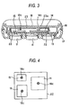
- Fig. 3 is a cross sectional view showing a portable telephone set according to a second embodiment of the invention.
- the second embodiment employs protecting bosses (protrusion portion) 18c protruded from the rear case 18 instead of the protecting boss 18b of the rear case 18, which is employed in the first embodiment shown in Fig. 2, and those protecting bosses press down the BGA packages 14, 15 and 16 against the printed circuit board 13.
- Fig. 4 show the shape. and positions of the protecting bosses 18c when the bosses press down the surfaces of the BGA packages 14, 15 and 16.
- Boss insertion holes 23a are formed at positions of the shield cover 23, which correspond respectively to the central parts of the BGA packages 14, 15 and 16.
- the protecting bosses 18c extend from the rear case 18, pass through the boss insertion holes 23a and reach the surfaces of the BGA packages 14, 15 and 16.
- the tip of each of the protecting bosses 18c is brought into close contact with the surface of each of the BGA packages 14, 15 and 16. Actually, however, a slight gap is present between them as shown in Fig. 3 since production tolerances of the related component parts are present.
- the gap is small, about 0.1mm. Therefore, even if the printed circuit board 13 is deformed a distance close in value to the soldering part by the depressing force to the push button 11, the peeling-off of the soldering part does not occur.
- the rear case 18 restricts a further deformation of the printed circuit board 13 which exceeds the gap. Consequently, the soldering part can be maintained in good conditions with lapse of time.
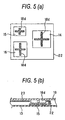
- Figs. 5(a) and 5(b) and Figs. 6(a) and 6(b) are explanatory diagrams for explaining embodiments of the invention in which shapes of the protecting bosses are each changed from that of the already described one.
- the protecting bosses hold down the BGA packages at wider areas, so that the holding effect of the BGA packages is increased.
- the size increase of the protecting bosses possibly hinders heat radiation of the BGA packages, and increases material cost and the weight of the portable telephone set.
- the surfaces of the BGA packages 14, 15 and 16 are held down with protecting bosses 18d each shaped like a cross.
- the surfaces of the BGA packages 14, 15 and 16 are held down with protecting bosses 18e each shaped like a rectangle. Since the protecting bosses are cross or rectangle shaped, the protecting bosses do not hinder the heat radiation of the BGA packages.
- Fig. 7 is a cross sectional view showing a portable telephone set according to a third embodiment of the invention.
- the instant embodiment is featured substantially by a combination of the feature of the first embodiment (the protrusion portion 18b formed along the shield wall 22 shown in Fig. 2) and the feature of the second embodiment (the protecting bosses 18c shown in Fig. 3). It is evident that the protecting bosses 18d and 18e shown in Figs. 5 and' 6 may be used for the protecting bosses.
- the third embodiment has both the features of the first and second embodiments, those features synergistically act to more lessen the stress applied to the soldering parts of the BGA packages 14, 15 and 16. Therefore, even when the push button 11 is repeatedly and frequently depressed, the soldering parts can be maintained in good conditions for a long period of time.
- the soldering parts of the BGA packages mounted on the back side of the operation button can be maintained in good conditions. As a result, a reliability of the portable electronic device is improved.
Landscapes
- Engineering & Computer Science (AREA)
- Microelectronics & Electronic Packaging (AREA)
- Signal Processing (AREA)
- Telephone Set Structure (AREA)
- Shielding Devices Or Components To Electric Or Magnetic Fields (AREA)
- Push-Button Switches (AREA)
- Casings For Electric Apparatus (AREA)
- Mounting Of Printed Circuit Boards And The Like (AREA)
- Mounting Components In General For Electric Apparatus (AREA)
Abstract
Description
Claims (5)
- A portable electronic device in which microswitches controlled by operation buttons are mounted on one side of a printed circuit board, and circuit elements accommodated in BGA packages are soldered on the other side of said printed circuit board, said portable electronic device is characterized in that:a shield wall for surrounding said BGA packages is mounted on said printed circuit board, and a protrusion portion for holding down said shield wall on said printed circuit board is protruded from a case of said portable electronic device.
- A portable electronic device in which microswitches controlled by operation buttons are mounted on one side of a printed circuit board, and circuit elements accommodated in BGA packages are soldered on the other side of said printed circuit board, said portable electronic device is characterized in that:a protrusion portion for holding down surfaces of said BGA packages on said printed circuit board is protruded from said case of said portable electronic device.
- A portable electronic device in which microswitches controlled by operation buttons are mounted on one side of a printed circuit board, and circuit elements accommodated in BGA packages are soldered on the other side of said printed circuit board, said portable electronic device is characterized in that:a shield wall for surrounding said BGA packages is mounted on said printed circuit board;a first protrusion portion for holding down said shield wall on said printed circuit board is protruded from a case of said portable electronic device; anda second protrusion portion for holding down surfaces of said BGA packages on said printed circuit board is protruded from said case of said portable electronic device.
- A BGA package protecting device for protecting soldering parts of a BGA package soldered on a printed circuit board, said BGA package protecting device is characterized in that:a shield wall for surrounding said BGA packages is mounted on said printed circuit board; anda member for holding down said shield wall on said printed circuit board along said shield wall is provided.
- A BGA package protecting device for protecting soldering parts of a BGA package soldered on a printed circuit board, said BGA package protecting device is characterized in that:a shield wall for surrounding said BGA packages is mounted on said printed circuit board; anda case of said portable electronic device includes a first member for holding down said shield wall on said printed circuit board and second members for holding down surfaces of said BGA packages on said printed circuit board.
Applications Claiming Priority (3)
| Application Number | Priority Date | Filing Date | Title |
|---|---|---|---|
| JP2001279871 | 2001-09-14 | ||
| JP2001279871A JP4601879B2 (en) | 2001-09-14 | 2001-09-14 | Portable electronic device and BGA package protection device |
| PCT/JP2002/005687 WO2003026372A1 (en) | 2001-09-14 | 2002-06-07 | Portable electronic apparatus and bga package protective device |
Publications (2)
| Publication Number | Publication Date |
|---|---|
| EP1427268A1 true EP1427268A1 (en) | 2004-06-09 |
| EP1427268A4 EP1427268A4 (en) | 2008-07-02 |
Family
ID=19103968
Family Applications (1)
| Application Number | Title | Priority Date | Filing Date |
|---|---|---|---|
| EP02733410A Withdrawn EP1427268A4 (en) | 2001-09-14 | 2002-06-07 | PORTABLE ELECTRONIC APPARATUS AND DEVICE FOR PROTECTING A BGA ASSEMBLY |
Country Status (5)
| Country | Link |
|---|---|
| US (1) | US7436676B2 (en) |
| EP (1) | EP1427268A4 (en) |
| JP (1) | JP4601879B2 (en) |
| CN (1) | CN100348081C (en) |
| WO (1) | WO2003026372A1 (en) |
Cited By (1)
| Publication number | Priority date | Publication date | Assignee | Title |
|---|---|---|---|---|
| EP2498586A3 (en) * | 2011-03-11 | 2013-08-28 | Funai Electric Co., Ltd. | Flexible Flat Cable and Image Display Device |
Families Citing this family (12)
| Publication number | Priority date | Publication date | Assignee | Title |
|---|---|---|---|---|
| JP4556174B2 (en) * | 2004-12-15 | 2010-10-06 | 日本電気株式会社 | Portable terminal device and heat dissipation method |
| JP2006302072A (en) * | 2005-04-22 | 2006-11-02 | Matsushita Electric Ind Co Ltd | Portable information processing device |
| US20090052686A1 (en) * | 2007-08-23 | 2009-02-26 | Fortemedia, Inc. | Electronic device with an internal microphone array |
| JP2009117661A (en) * | 2007-11-07 | 2009-05-28 | Tokai Rika Co Ltd | Printed circuit board |
| JP4267677B1 (en) * | 2008-01-15 | 2009-05-27 | パナソニック株式会社 | Electronics |
| US7952881B2 (en) * | 2009-03-31 | 2011-05-31 | Motorola Solutions, Inc. | Thermal-electrical assembly for a portable communication device |
| BR202012004685Y1 (en) | 2011-07-13 | 2019-04-02 | Google Technology Holdings LLC | MOBILE ELECTRONIC DEVICE WITH IMPROVED LAMINATED CONSTRUCTION |
| BR202012004687U8 (en) | 2011-07-13 | 2016-11-22 | Motorola Mobility Inc | MOBILE ELECTRONIC DEVICE WITH IMPROVED CHASSIS |
| BR202012004686Y1 (en) | 2011-07-13 | 2019-05-14 | Google Technology Holdings LLC | MOBILE ELECTRONIC DEVICE WITH ENHANCED IMPACT REDUCTION. |
| KR200471325Y1 (en) * | 2011-07-13 | 2014-02-19 | 모토로라 모빌리티 엘엘씨 | Mobile electronic device with enhanced tolerance accumulator |
| KR20140142600A (en) * | 2013-06-04 | 2014-12-12 | 삼성전자주식회사 | Protection apparatus of electronic device and electronic device having the same |
| KR20160039999A (en) * | 2014-10-02 | 2016-04-12 | 삼성전자주식회사 | Electronic device |
Family Cites Families (23)
| Publication number | Priority date | Publication date | Assignee | Title |
|---|---|---|---|---|
| JPS59119673U (en) * | 1983-01-31 | 1984-08-13 | ソニー株式会社 | display device |
| JPS63102299A (en) * | 1986-10-17 | 1988-05-07 | 松下電器産業株式会社 | Remote controller |
| JPH062307Y2 (en) * | 1988-05-31 | 1994-01-19 | 東京電気株式会社 | Two circuit board built-in electrical components |
| US4890199A (en) * | 1988-11-04 | 1989-12-26 | Motorola, Inc. | Miniature shield with opposing cantilever spring fingers |
| JP2887956B2 (en) * | 1991-07-11 | 1999-05-10 | 日本電気株式会社 | Portable radio |
| EP0727932B1 (en) * | 1994-11-28 | 1999-04-07 | Kabushiki Kaisha Toshiba | Electromagnetic shielded casing |
| FR2737068B1 (en) * | 1995-07-18 | 1997-10-03 | Alcatel Mobile Comm France | COMMUNICATION APPARATUS WITH ELECTROSTATIC PROTECTION |
| US5596487A (en) * | 1995-07-31 | 1997-01-21 | Motorola, Inc. | Apparatus for RF shielding radio circuitry |
| JP3136298B2 (en) * | 1996-07-17 | 2001-02-19 | 株式会社日立国際電気 | Mobile device shield structure |
| IN192428B (en) | 1996-09-26 | 2004-04-24 | Matsushita Electric Industrial Co Ltd | |
| GB2327537B (en) * | 1997-07-18 | 2002-05-22 | Nokia Mobile Phones Ltd | Electronic device |
| US6058293A (en) * | 1997-09-12 | 2000-05-02 | Ericsson, Inc. | Frame structure for cellular telephones |
| US6063999A (en) * | 1997-12-19 | 2000-05-16 | Siemens Medical Systems, Inc. | Surface mount spring gasket and EMI enclosure |
| EP0951161A1 (en) * | 1998-04-16 | 1999-10-20 | Koninklijke Philips Electronics N.V. | Contact device for connecting a liquid crystal display to a printed circuit board |
| JP3747997B2 (en) * | 1998-11-10 | 2006-02-22 | 松下電器産業株式会社 | Mobile terminal device |
| FI106904B (en) * | 1998-12-08 | 2001-04-30 | Nokia Mobile Phones Ltd | Wireless communication means and control means |
| JP2000236378A (en) * | 1999-02-16 | 2000-08-29 | Matsushita Electric Ind Co Ltd | Mobile phone equipment |
| US6624432B1 (en) * | 1999-10-12 | 2003-09-23 | Shielding For Electronics, Inc. | EMI containment apparatus |
| JP2001237585A (en) * | 2000-02-22 | 2001-08-31 | Murata Mfg Co Ltd | Electronic component and manufacturing method thereof |
| JP2002008606A (en) * | 2000-06-21 | 2002-01-11 | Sony Corp | Battery pack and personal digital assistant |
| US6570776B2 (en) * | 2001-06-20 | 2003-05-27 | Ericsson, Inc. | Shielded electronics package structure with enhanced mechanical reliability |
| JP2003060365A (en) * | 2001-08-21 | 2003-02-28 | Mitsubishi Electric Corp | Mobile terminal |
| JP4186732B2 (en) * | 2003-07-24 | 2008-11-26 | 株式会社村田製作所 | Electronics |
-
2001
- 2001-09-14 JP JP2001279871A patent/JP4601879B2/en not_active Expired - Fee Related
-
2002
- 2002-06-07 CN CNB028177894A patent/CN100348081C/en not_active Expired - Fee Related
- 2002-06-07 EP EP02733410A patent/EP1427268A4/en not_active Withdrawn
- 2002-06-07 US US10/489,498 patent/US7436676B2/en not_active Expired - Fee Related
- 2002-06-07 WO PCT/JP2002/005687 patent/WO2003026372A1/en not_active Ceased
Cited By (1)
| Publication number | Priority date | Publication date | Assignee | Title |
|---|---|---|---|---|
| EP2498586A3 (en) * | 2011-03-11 | 2013-08-28 | Funai Electric Co., Ltd. | Flexible Flat Cable and Image Display Device |
Also Published As
| Publication number | Publication date |
|---|---|
| CN1554216A (en) | 2004-12-08 |
| EP1427268A4 (en) | 2008-07-02 |
| JP2003086971A (en) | 2003-03-20 |
| JP4601879B2 (en) | 2010-12-22 |
| US7436676B2 (en) | 2008-10-14 |
| WO2003026372A1 (en) | 2003-03-27 |
| US20040235538A1 (en) | 2004-11-25 |
| CN100348081C (en) | 2007-11-07 |
Similar Documents
| Publication | Publication Date | Title |
|---|---|---|
| US7436676B2 (en) | Portable electronic apparatus and BGA package protective device | |
| US9450631B2 (en) | Case for a hand held device | |
| US7710716B2 (en) | Electronic apparatus | |
| JP2005025273A5 (en) | ||
| US20030153282A1 (en) | Mobile phone with replaceable key assemblies | |
| JP7464095B2 (en) | Electronic clock | |
| JP4357579B1 (en) | Electronics | |
| US8124902B2 (en) | Push button switch | |
| KR100768269B1 (en) | Uppercase unified with buttons and personal portable device having the uppercase | |
| JP2002008606A (en) | Battery pack and personal digital assistant | |
| JP4610518B2 (en) | Display unit and portable terminal equipped with the same | |
| TWI401718B (en) | Compound operation type input device | |
| TWI250798B (en) | Pushbutton protection device of electronic product | |
| JP2003060365A (en) | Mobile terminal | |
| CN2899546Y (en) | Protective jacket for electronics | |
| JP4480243B2 (en) | Operation key structure and electronic device | |
| JP3560621B2 (en) | Attachment structure of operation member to mating portion of split housing and sound generating device provided with this attachment structure | |
| JP2018121197A (en) | Remote control device | |
| CN101512698B (en) | Portable electronic device | |
| JP2001143554A (en) | Multi-way operating switch and movable telephone having multi-way operating switch | |
| ATE538428T1 (en) | PORTABLE ELECTRONIC COMMUNICATION DEVICE WITH METAL KEYPAD | |
| JP2002307347A (en) | Portable teaching device | |
| JPH10301178A (en) | Optical equipment | |
| JP2000078253A (en) | Portable mobile terminal | |
| JP2003297174A (en) | Switch and touch panel therefor |
Legal Events
| Date | Code | Title | Description |
|---|---|---|---|
| PUAI | Public reference made under article 153(3) epc to a published international application that has entered the european phase |
Free format text: ORIGINAL CODE: 0009012 |
|
| 17P | Request for examination filed |
Effective date: 20040315 |
|
| AK | Designated contracting states |
Kind code of ref document: A1 Designated state(s): AT BE CH CY DE DK ES FI FR GB GR IE IT LI LU MC NL PT SE TR |
|
| AX | Request for extension of the european patent |
Extension state: AL LT LV MK RO SI |
|
| A4 | Supplementary search report drawn up and despatched |
Effective date: 20080602 |
|
| RAP1 | Party data changed (applicant data changed or rights of an application transferred) |
Owner name: PANASONIC CORPORATION |
|
| 17Q | First examination report despatched |
Effective date: 20100809 |
|
| GRAP | Despatch of communication of intention to grant a patent |
Free format text: ORIGINAL CODE: EPIDOSNIGR1 |
|
| RIC1 | Information provided on ipc code assigned before grant |
Ipc: H05K 9/00 20060101AFI20120626BHEP Ipc: H04M 1/23 20060101ALI20120626BHEP |
|
| STAA | Information on the status of an ep patent application or granted ep patent |
Free format text: STATUS: THE APPLICATION IS DEEMED TO BE WITHDRAWN |
|
| 18D | Application deemed to be withdrawn |
Effective date: 20121120 |