EP1427196B1 - Bildaufnahmevorrichtung - Google Patents
Bildaufnahmevorrichtung Download PDFInfo
- Publication number
- EP1427196B1 EP1427196B1 EP03104319.3A EP03104319A EP1427196B1 EP 1427196 B1 EP1427196 B1 EP 1427196B1 EP 03104319 A EP03104319 A EP 03104319A EP 1427196 B1 EP1427196 B1 EP 1427196B1
- Authority
- EP
- European Patent Office
- Prior art keywords
- gain
- image
- signal
- pickup device
- image pickup
- Prior art date
- Legal status (The legal status is an assumption and is not a legal conclusion. Google has not performed a legal analysis and makes no representation as to the accuracy of the status listed.)
- Expired - Lifetime
Links
Images
Classifications
-
- H—ELECTRICITY
- H04—ELECTRIC COMMUNICATION TECHNIQUE
- H04N—PICTORIAL COMMUNICATION, e.g. TELEVISION
- H04N25/00—Circuitry of solid-state image sensors [SSIS]; Control thereof
- H04N25/50—Control of the SSIS exposure
- H04N25/57—Control of the dynamic range
-
- H—ELECTRICITY
- H04—ELECTRIC COMMUNICATION TECHNIQUE
- H04N—PICTORIAL COMMUNICATION, e.g. TELEVISION
- H04N25/00—Circuitry of solid-state image sensors [SSIS]; Control thereof
- H04N25/70—SSIS architectures; Circuits associated therewith
- H04N25/71—Charge-coupled device [CCD] sensors; Charge-transfer registers specially adapted for CCD sensors
- H04N25/745—Circuitry for generating timing or clock signals
-
- H—ELECTRICITY
- H04—ELECTRIC COMMUNICATION TECHNIQUE
- H04N—PICTORIAL COMMUNICATION, e.g. TELEVISION
- H04N23/00—Cameras or camera modules comprising electronic image sensors; Control thereof
- H04N23/70—Circuitry for compensating brightness variation in the scene
- H04N23/76—Circuitry for compensating brightness variation in the scene by influencing the image signals
-
- H—ELECTRICITY
- H04—ELECTRIC COMMUNICATION TECHNIQUE
- H04N—PICTORIAL COMMUNICATION, e.g. TELEVISION
- H04N25/00—Circuitry of solid-state image sensors [SSIS]; Control thereof
- H04N25/60—Noise processing, e.g. detecting, correcting, reducing or removing noise
- H04N25/62—Detection or reduction of noise due to excess charges produced by the exposure, e.g. smear, blooming, ghost image, crosstalk or leakage between pixels
Definitions
- the invention relates to an image pickup device, notably a camera.
- An image pickup device for instance a still-picture camera or a video camera, has an image sensor, which generates an electrical signal (image signal) describing the light impinging on the image sensor, i.e. an image of the scene facing the image sensor.
- the image sensor is fed by a pulse pattern generator, which generates driving signals (operating voltages and various clocks) needed for operation of the image sensor.
- the image signal generated by the image sensor is amplified at a gain, which is directly or indirectly selected by the user of the image receiver through adjusting means.
- Image sensors are generally designed to handle overexposure, up to a value called maximum charge handling capacity Q max , for instance 400 %. At high gain settings, this overexposure capability leads to huge values (at 12 dB, 1600 %) of the amplified signal, thereby generating unacceptable ringing and streaking. Furthermore, high gain also implies more noise in the amplified signal.
- JP 01-264 481 discloses an apparatus for improving the efficiency in transferring charge carriers in a charge coupled device (CCD).
- the apparatus is adapted to change the depth of the potential well of a CCD transfer part in accordance with the quantity of the carriers to be generated by accordingly controlling the potential differences between adjoining electrodes in the transfer part of the CCD.
- an image pickup device comprising an image sensor generating an image signal, driving means generating a driving signal for the image sensor, an amplifier for amplifying the image signal with a given gain, adjusting means to set the gain and control means to control the pulse amplitude of the driving signal depending on the gain as defined by the subject-matter of claim 1.
- the corresponding method for controlling an image pickup device is defined by the subject-matter of claim 8.
- control of the power of the driving signal makes it possible to lower the maximum possible signal at high gains, and therefore to reduce ringing and streaking.
- the invention thus proposes an image pickup device comprising an image sensor generating an image signal, driving means generating a signal with pulses for driving the image sensor, an amplifier for amplifying the image signal with a given gain, adjusting means to set the gain and control means to set the pulse height depending on the gain.
- the driving signal is a storage clock signal or an image clock signal.
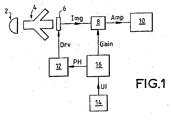
- FIG. 1 represents the main elements of a video camera according to the invention.
- This video camera is a colour video camera with 3 image sensors (3 CCD imagers) and corresponding processing channels, but only 1 image sensor and its corresponding processing channel have been represented for the sake of conciseness.
- the invention similarly applies to the other 2 channels.
- Optical means 2 (here represented as a lens) directs incoming light to CCD imagers (image sensors) through a colour separator 4, and notably to a CCD imager referenced 6.
- a pulse pattern generator 12 supplies various operating voltages and clocks (for instance an image clock and a storage clock), generally denominated driving signals Drv, to the CCD imager 6. Thanks to these driving signals Drv provided by the pulse pattern generator 12, the CCD imager 6 generates an image signal Img representing the quantity of light received by the CCD image 6 on each of its pixel element.
- the image signal Img is transmitted to an amplifier 8, which outputs an amplified image signal Amp.
- the amplified image signal Amp is received at a processing stage 10, where it is processed and/or recorded on a medium and/or broadcast to other users.
- the processing stage 10 also receives amplified signals from the other 2 colour channels (not represented).
- the amplifier 8 pre-forms the image signal, for instance by correlated double sampling.
- the amplifier 8 also provides a gain controlled by gain control signal Gain received from a main controller 16.
- the main controller 16 generates the gain control signal Gain based on a value UI set by the user through a user interface 14.
- the main processor computes a pulse height PH and transmits it to the pulse pattern generator 12.
- the pulse height can be selected between a limited number of possible values depending on the gain: 12 V for a gain between 0 dB and 4 dB, 10 V between 4 dB and 10 dB, 8 V for more than 10 dB.
- the pulse pattern generator 12 generates the driving signals Drv based on the signal PH received from the main controller 16. Notably, the pulse pattern generator 12 generates an image clock (image gate voltages) for the 3 CCD imagers (and notably for CCD imager 6) with a high level equal to the pulse height PH received from the main controller 16.
- image clock image gate voltages
- the storage clock has a pulse height having the value PH, and thus dependent on the gain.
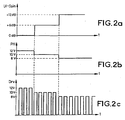
- Figure 2a represents variations of the gain of the amplifier 8 in accordance with commands UI for the user.
- Figure 2b represents the corresponding variations of the pulse height signal PH.
- the pulse height signal PH is a decreasing function of the gain. Therefore, when the gain increases, the pulse height PH decreases.
- Figure 2c represents the image clock driving signal Drv applied as a voltage to the image gate of the CCD imager 6.
- the driving signal is a train of pulses which height is determined by the value PH computed based on the gain. ( Figure 2c is explanative only; its timescale is not realistic.)
- the main controller 16 can transmit to the pulse pattern generator 12 a value indicative of the gain of the amplifier 8 and the pulse pattern generator 12 then computes the pulse height of the driving signal(s) based on this value.
- the main controller 16 and the pulse pattern generator are made as a single entity, for instance as a single integrated circuit.
Landscapes
- Engineering & Computer Science (AREA)
- Multimedia (AREA)
- Signal Processing (AREA)
- Transforming Light Signals Into Electric Signals (AREA)
- Studio Devices (AREA)
- Apparatus For Radiation Diagnosis (AREA)
Claims (8)
- Bildaufnahmevorrichtung mit:- einem Bildsensor (6), der ein Bildsignal (Img) erzeugt,- einem Ansteuermittel (12), das ein Ansteuersignal (Drv) für den Bildsensor (6) erzeugt,- einem Verstärker (8) zum Verstärken des Bildsignals (Img) mit einem vorgegebenen Verstärkungsfaktor (Gain),- einem Justiermittel (14, 16) zum Einstellen des Verstärkungsfaktors (Gain),gekennzeichnet durch ein Regelmittel (12; 16), das so ausgelegt ist, dass es die Impulsamplitude des Ansteuersignals (Drv) als abfallende Funktion des Verstärkungsfaktors (Gain) regelt.
- Bildaufnahmevorrichtung nach Anspruch 1, bei der ein Bitmustergenerator (12) das Ansteuermittel aufweist.
- Bildaufnahmevorrichtung nach Anspruch 2, bei der der Bitmustergenerator (12) das Regelmittel aufweist.
- Bildaufnahmevorrichtung nach Anspruch 1 oder 2, bei der eine Steuereinheit (16) das Regelmittel umfasst.
- Bildaufnahmevorrichtung nach einem der Ansprüche 1 bis 4, bei der es sich bei dem Ansteuersignal (Drv) um ein Speichertaktsignal oder ein Bildtaktsignal handelt.
- Bildaufnahmevorrichtung nach einem der Ansprüche 1 bis 5, bei der es sich bei dem Bildsensor (6) um einen CCD-Bildsensor handelt.
- Bildaufnahmevorrichtung nach einem der Ansprüche 1 bis 6, die zwei weitere Bildsensoren umfasst.
- Verfahren zum Steuern einer Bildaufnahmevorrichtung mit folgenden Schritten:- Erzeugen eines Bildsignals (Img) in einem Bildsensor (6),- Einstellen eines Verstärkungsfaktors (Gain), der auf das Bildsignal (Img) angewendet wird,- Verstärken des Bildsignals (Img) mit dem eingestellten Verstärkungsfaktor (Gain),wobei das Verfahren ferner Folgendes umfasst:- Regeln eines maximalen Ausgangssignals des Bildsensors (6) durch Regeln der Impulsamplitude eines Ansteuersignals (Drv) für den Bildsensor (6) als abfallender Funktion des Verstärkungsfaktors (Gain).
Priority Applications (1)
| Application Number | Priority Date | Filing Date | Title |
|---|---|---|---|
| EP03104319.3A EP1427196B1 (de) | 2002-12-06 | 2003-11-21 | Bildaufnahmevorrichtung |
Applications Claiming Priority (3)
| Application Number | Priority Date | Filing Date | Title |
|---|---|---|---|
| EP02293012 | 2002-12-06 | ||
| EP02293012A EP1427195A1 (de) | 2002-12-06 | 2002-12-06 | Bildaufnahmevorrichtung |
| EP03104319.3A EP1427196B1 (de) | 2002-12-06 | 2003-11-21 | Bildaufnahmevorrichtung |
Publications (2)
| Publication Number | Publication Date |
|---|---|
| EP1427196A1 EP1427196A1 (de) | 2004-06-09 |
| EP1427196B1 true EP1427196B1 (de) | 2013-07-31 |
Family
ID=32309495
Family Applications (2)
| Application Number | Title | Priority Date | Filing Date |
|---|---|---|---|
| EP02293012A Withdrawn EP1427195A1 (de) | 2002-12-06 | 2002-12-06 | Bildaufnahmevorrichtung |
| EP03104319.3A Expired - Lifetime EP1427196B1 (de) | 2002-12-06 | 2003-11-21 | Bildaufnahmevorrichtung |
Family Applications Before (1)
| Application Number | Title | Priority Date | Filing Date |
|---|---|---|---|
| EP02293012A Withdrawn EP1427195A1 (de) | 2002-12-06 | 2002-12-06 | Bildaufnahmevorrichtung |
Country Status (7)
| Country | Link |
|---|---|
| US (1) | US7486316B2 (de) |
| EP (2) | EP1427195A1 (de) |
| JP (1) | JP2004194318A (de) |
| KR (1) | KR101005444B1 (de) |
| CN (1) | CN100435563C (de) |
| MY (1) | MY142661A (de) |
| TW (1) | TWI292277B (de) |
Families Citing this family (4)
| Publication number | Priority date | Publication date | Assignee | Title |
|---|---|---|---|---|
| US8892163B2 (en) * | 2012-03-06 | 2014-11-18 | Omni Vision Technologies, Inc. | Image sensor having a pulsed mode of operation |
| EP3037913A4 (de) * | 2013-08-22 | 2017-05-17 | Samsung Electronics Co., Ltd. | Verfahren zur durchführung eines energiesparmodus bei einer elektronischen vorrichtung und elektronische vorrichtung dafür |
| US9547363B2 (en) * | 2014-07-16 | 2017-01-17 | Mediatek Inc. | Power-saving method and associated electronic device |
| CN105278655B (zh) * | 2015-11-03 | 2018-08-03 | 广东欧珀移动通信有限公司 | 指纹传感器的控制方法及装置 |
Family Cites Families (9)
| Publication number | Priority date | Publication date | Assignee | Title |
|---|---|---|---|---|
| US4635126A (en) * | 1981-12-18 | 1987-01-06 | Canon Kabushiki Kaisha | Image pick-up system |
| US4683498A (en) * | 1986-04-21 | 1987-07-28 | Rca Corporation | Compatible wide-screen television system camera |
| JPH0828839B2 (ja) * | 1987-04-21 | 1996-03-21 | オリンパス光学工業株式会社 | テレビカメラ装置 |
| JPH01264481A (ja) * | 1988-04-15 | 1989-10-20 | Toshiba Corp | ビデオカメラ |
| US5528291A (en) * | 1991-09-25 | 1996-06-18 | Fuji Photo Film Co., Ltd. | CCD image pickup device and method of driving which maintains sensitivity regardless of the operating mode |
| JPH06141328A (ja) * | 1992-10-28 | 1994-05-20 | Victor Co Of Japan Ltd | 自動感度調整装置 |
| US5625411A (en) * | 1992-12-22 | 1997-04-29 | Fuji Photo Film, Ltd. | Video camera printer apparatus and method of controlling same and apparatus and method for detecting print inhibit signal |
| US5986705A (en) * | 1997-02-18 | 1999-11-16 | Matsushita Electric Industrial Co., Ltd. | Exposure control system controlling a solid state image sensing device |
| US6958776B2 (en) * | 2000-07-12 | 2005-10-25 | Vanguard International Semiconductor Corp. | Method and apparatus of controlling a pixel reset level for reducing an image lag in a CMOS sensor |
-
2002
- 2002-12-06 EP EP02293012A patent/EP1427195A1/de not_active Withdrawn
-
2003
- 2003-11-21 TW TW092132660A patent/TWI292277B/zh not_active IP Right Cessation
- 2003-11-21 EP EP03104319.3A patent/EP1427196B1/de not_active Expired - Lifetime
- 2003-11-26 KR KR1020030084444A patent/KR101005444B1/ko not_active Expired - Fee Related
- 2003-11-26 US US10/723,553 patent/US7486316B2/en not_active Expired - Fee Related
- 2003-12-05 JP JP2003408085A patent/JP2004194318A/ja active Pending
- 2003-12-05 CN CNB2003101203096A patent/CN100435563C/zh not_active Expired - Fee Related
- 2003-12-05 MY MYPI20034672A patent/MY142661A/en unknown
Also Published As
| Publication number | Publication date |
|---|---|
| EP1427195A1 (de) | 2004-06-09 |
| US20040109073A1 (en) | 2004-06-10 |
| TW200410560A (en) | 2004-06-16 |
| CN100435563C (zh) | 2008-11-19 |
| US7486316B2 (en) | 2009-02-03 |
| TWI292277B (en) | 2008-01-01 |
| KR20040049792A (ko) | 2004-06-12 |
| KR101005444B1 (ko) | 2011-01-05 |
| MY142661A (en) | 2010-12-15 |
| CN1507271A (zh) | 2004-06-23 |
| EP1427196A1 (de) | 2004-06-09 |
| JP2004194318A (ja) | 2004-07-08 |
Similar Documents
| Publication | Publication Date | Title |
|---|---|---|
| Schanz et al. | A high-dynamic-range CMOS image sensor for automotive applications | |
| US8823849B2 (en) | Photoelectric conversion device and image capturing device having circuit for reducing offset generated by amplifiers | |
| EP1545123B1 (de) | Abbildungseinrichtung, abbildungseinrichtungs-bildausgabeverfahren und computerprogramm | |
| US7129985B1 (en) | Image sensing apparatus arranged on a single substrate | |
| KR20020060093A (ko) | 고체 촬상 장치 및 화상 입력 장치 | |
| JPWO2007108317A1 (ja) | 画像信号処理装置及び画像信号処理方法 | |
| US7714928B2 (en) | Image sensing apparatus and an image sensing method comprising a logarithmic characteristic area and a linear characteristic area | |
| EP1289276A1 (de) | Verfahren zur Übertragung von elektrischen Ladungen aus einem Bildsensor und Bildsensorsvorrichtung | |
| EP0862320A3 (de) | Einrichtung und Verfahren zur Kompensation von bei Datenkommunikation auftretender Verschiebungs- und Verstärkungsdrift | |
| JP2003032548A (ja) | 固体撮像装置及びそれを用いた撮像システム | |
| US7948531B2 (en) | Imaging apparatus and correction method of image data | |
| EP1427196B1 (de) | Bildaufnahmevorrichtung | |
| EP1511290B1 (de) | Festkörperbildaufnahmevorrichtung | |
| US7327500B2 (en) | Image inputting apparatus | |
| JP4154068B2 (ja) | 固体撮像装置及びそれを用いた撮像システム及び画像読取システム | |
| CN100385921C (zh) | 固体摄像装置、固体摄像元件的控制电路及控制方法 | |
| JP2010136253A (ja) | 撮像装置およびその制御方法 | |
| EP1079602A3 (de) | Bildeingabevorrichtung | |
| JP4795910B2 (ja) | 信号電荷の読出方法および固体撮像装置 | |
| US5781314A (en) | Color image reading apparatus and method | |
| EP0211441A2 (de) | Ladungsgekoppelte Verzögerungsleitung | |
| JP4011890B2 (ja) | 固体撮像装置 | |
| JP2005304009A (ja) | 電荷結合素子の電圧制御装置、および制御方法 | |
| CN1332566C (zh) | 成像装置和方法 | |
| KR100858073B1 (ko) | 자동 이득 제어 회로 |
Legal Events
| Date | Code | Title | Description |
|---|---|---|---|
| PUAI | Public reference made under article 153(3) epc to a published international application that has entered the european phase |
Free format text: ORIGINAL CODE: 0009012 |
|
| AK | Designated contracting states |
Kind code of ref document: A1 Designated state(s): AT BE BG CH CY CZ DE DK EE ES FI FR GB GR HU IE IT LI LU MC NL PT RO SE SI SK TR |
|
| AX | Request for extension of the european patent |
Extension state: AL LT LV MK |
|
| 17P | Request for examination filed |
Effective date: 20041118 |
|
| AKX | Designation fees paid |
Designated state(s): DE FR GB IT |
|
| RAP1 | Party data changed (applicant data changed or rights of an application transferred) |
Owner name: THOMSON LICENSING |
|
| 17Q | First examination report despatched |
Effective date: 20071030 |
|
| RAP1 | Party data changed (applicant data changed or rights of an application transferred) |
Owner name: THOMSON LICENSING |
|
| RAP1 | Party data changed (applicant data changed or rights of an application transferred) |
Owner name: GVBB HOLDINGS S.A.R.L |
|
| REG | Reference to a national code |
Ref country code: DE Ref legal event code: R079 Ref document number: 60344600 Country of ref document: DE Free format text: PREVIOUS MAIN CLASS: H04N0005335000 Ipc: H04N0005359000 |
|
| GRAP | Despatch of communication of intention to grant a patent |
Free format text: ORIGINAL CODE: EPIDOSNIGR1 |
|
| RIC1 | Information provided on ipc code assigned before grant |
Ipc: H04N 5/359 20110101AFI20130208BHEP Ipc: H04N 5/376 20110101ALI20130208BHEP |
|
| GRAS | Grant fee paid |
Free format text: ORIGINAL CODE: EPIDOSNIGR3 |
|
| GRAA | (expected) grant |
Free format text: ORIGINAL CODE: 0009210 |
|
| AK | Designated contracting states |
Kind code of ref document: B1 Designated state(s): DE FR GB IT |
|
| REG | Reference to a national code |
Ref country code: GB Ref legal event code: FG4D |
|
| REG | Reference to a national code |
Ref country code: DE Ref legal event code: R096 Ref document number: 60344600 Country of ref document: DE Effective date: 20130926 |
|
| PG25 | Lapsed in a contracting state [announced via postgrant information from national office to epo] |
Ref country code: IT Free format text: LAPSE BECAUSE OF FAILURE TO SUBMIT A TRANSLATION OF THE DESCRIPTION OR TO PAY THE FEE WITHIN THE PRESCRIBED TIME-LIMIT Effective date: 20130731 |
|
| PLBE | No opposition filed within time limit |
Free format text: ORIGINAL CODE: 0009261 |
|
| STAA | Information on the status of an ep patent application or granted ep patent |
Free format text: STATUS: NO OPPOSITION FILED WITHIN TIME LIMIT |
|
| 26N | No opposition filed |
Effective date: 20140502 |
|
| REG | Reference to a national code |
Ref country code: DE Ref legal event code: R097 Ref document number: 60344600 Country of ref document: DE Effective date: 20140502 |
|
| PGFP | Annual fee paid to national office [announced via postgrant information from national office to epo] |
Ref country code: GB Payment date: 20141127 Year of fee payment: 12 Ref country code: DE Payment date: 20141125 Year of fee payment: 12 |
|
| PGFP | Annual fee paid to national office [announced via postgrant information from national office to epo] |
Ref country code: FR Payment date: 20141217 Year of fee payment: 12 |
|
| REG | Reference to a national code |
Ref country code: DE Ref legal event code: R119 Ref document number: 60344600 Country of ref document: DE |
|
| GBPC | Gb: european patent ceased through non-payment of renewal fee |
Effective date: 20151121 |
|
| REG | Reference to a national code |
Ref country code: FR Ref legal event code: ST Effective date: 20160729 |
|
| PG25 | Lapsed in a contracting state [announced via postgrant information from national office to epo] |
Ref country code: DE Free format text: LAPSE BECAUSE OF NON-PAYMENT OF DUE FEES Effective date: 20160601 Ref country code: GB Free format text: LAPSE BECAUSE OF NON-PAYMENT OF DUE FEES Effective date: 20151121 |
|
| PG25 | Lapsed in a contracting state [announced via postgrant information from national office to epo] |
Ref country code: FR Free format text: LAPSE BECAUSE OF NON-PAYMENT OF DUE FEES Effective date: 20151130 |