EP1427093A1 - Multi-output dc-dc converter - Google Patents
Multi-output dc-dc converter Download PDFInfo
- Publication number
- EP1427093A1 EP1427093A1 EP02765428A EP02765428A EP1427093A1 EP 1427093 A1 EP1427093 A1 EP 1427093A1 EP 02765428 A EP02765428 A EP 02765428A EP 02765428 A EP02765428 A EP 02765428A EP 1427093 A1 EP1427093 A1 EP 1427093A1
- Authority
- EP
- European Patent Office
- Prior art keywords
- output
- stepped
- circuit
- main switch
- inverted
- Prior art date
- Legal status (The legal status is an assumption and is not a legal conclusion. Google has not performed a legal analysis and makes no representation as to the accuracy of the status listed.)
- Withdrawn
Links
Images




Classifications
-
- H—ELECTRICITY
- H02—GENERATION; CONVERSION OR DISTRIBUTION OF ELECTRIC POWER
- H02M—APPARATUS FOR CONVERSION BETWEEN AC AND AC, BETWEEN AC AND DC, OR BETWEEN DC AND DC, AND FOR USE WITH MAINS OR SIMILAR POWER SUPPLY SYSTEMS; CONVERSION OF DC OR AC INPUT POWER INTO SURGE OUTPUT POWER; CONTROL OR REGULATION THEREOF
- H02M3/00—Conversion of DC power input into DC power output
- H02M3/02—Conversion of DC power input into DC power output without intermediate conversion into AC
- H02M3/04—Conversion of DC power input into DC power output without intermediate conversion into AC by static converters
- H02M3/10—Conversion of DC power input into DC power output without intermediate conversion into AC by static converters using discharge tubes with control electrode or semiconductor devices with control electrode
- H02M3/145—Conversion of DC power input into DC power output without intermediate conversion into AC by static converters using discharge tubes with control electrode or semiconductor devices with control electrode using devices of a triode or transistor type requiring continuous application of a control signal
- H02M3/155—Conversion of DC power input into DC power output without intermediate conversion into AC by static converters using discharge tubes with control electrode or semiconductor devices with control electrode using devices of a triode or transistor type requiring continuous application of a control signal using semiconductor devices only
- H02M3/156—Conversion of DC power input into DC power output without intermediate conversion into AC by static converters using discharge tubes with control electrode or semiconductor devices with control electrode using devices of a triode or transistor type requiring continuous application of a control signal using semiconductor devices only with automatic control of output voltage or current, e.g. switching regulators
- H02M3/158—Conversion of DC power input into DC power output without intermediate conversion into AC by static converters using discharge tubes with control electrode or semiconductor devices with control electrode using devices of a triode or transistor type requiring continuous application of a control signal using semiconductor devices only with automatic control of output voltage or current, e.g. switching regulators including plural semiconductor devices as final control devices for a single load
- H02M3/1584—Conversion of DC power input into DC power output without intermediate conversion into AC by static converters using discharge tubes with control electrode or semiconductor devices with control electrode using devices of a triode or transistor type requiring continuous application of a control signal using semiconductor devices only with automatic control of output voltage or current, e.g. switching regulators including plural semiconductor devices as final control devices for a single load with a plurality of power processing stages connected in parallel
-
- H—ELECTRICITY
- H02—GENERATION; CONVERSION OR DISTRIBUTION OF ELECTRIC POWER
- H02M—APPARATUS FOR CONVERSION BETWEEN AC AND AC, BETWEEN AC AND DC, OR BETWEEN DC AND DC, AND FOR USE WITH MAINS OR SIMILAR POWER SUPPLY SYSTEMS; CONVERSION OF DC OR AC INPUT POWER INTO SURGE OUTPUT POWER; CONTROL OR REGULATION THEREOF
- H02M3/00—Conversion of DC power input into DC power output
- H02M3/02—Conversion of DC power input into DC power output without intermediate conversion into AC
- H02M3/04—Conversion of DC power input into DC power output without intermediate conversion into AC by static converters
- H02M3/10—Conversion of DC power input into DC power output without intermediate conversion into AC by static converters using discharge tubes with control electrode or semiconductor devices with control electrode
- H02M3/145—Conversion of DC power input into DC power output without intermediate conversion into AC by static converters using discharge tubes with control electrode or semiconductor devices with control electrode using devices of a triode or transistor type requiring continuous application of a control signal
- H02M3/155—Conversion of DC power input into DC power output without intermediate conversion into AC by static converters using discharge tubes with control electrode or semiconductor devices with control electrode using devices of a triode or transistor type requiring continuous application of a control signal using semiconductor devices only
- H02M3/156—Conversion of DC power input into DC power output without intermediate conversion into AC by static converters using discharge tubes with control electrode or semiconductor devices with control electrode using devices of a triode or transistor type requiring continuous application of a control signal using semiconductor devices only with automatic control of output voltage or current, e.g. switching regulators
- H02M3/158—Conversion of DC power input into DC power output without intermediate conversion into AC by static converters using discharge tubes with control electrode or semiconductor devices with control electrode using devices of a triode or transistor type requiring continuous application of a control signal using semiconductor devices only with automatic control of output voltage or current, e.g. switching regulators including plural semiconductor devices as final control devices for a single load
- H02M3/1582—Buck-boost converters
-
- H—ELECTRICITY
- H02—GENERATION; CONVERSION OR DISTRIBUTION OF ELECTRIC POWER
- H02M—APPARATUS FOR CONVERSION BETWEEN AC AND AC, BETWEEN AC AND DC, OR BETWEEN DC AND DC, AND FOR USE WITH MAINS OR SIMILAR POWER SUPPLY SYSTEMS; CONVERSION OF DC OR AC INPUT POWER INTO SURGE OUTPUT POWER; CONTROL OR REGULATION THEREOF
- H02M1/00—Details of apparatus for conversion
- H02M1/0067—Converter structures employing plural converter units, other than for parallel operation of the units on a single load
- H02M1/007—Plural converter units in cascade
-
- H—ELECTRICITY
- H02—GENERATION; CONVERSION OR DISTRIBUTION OF ELECTRIC POWER
- H02M—APPARATUS FOR CONVERSION BETWEEN AC AND AC, BETWEEN AC AND DC, OR BETWEEN DC AND DC, AND FOR USE WITH MAINS OR SIMILAR POWER SUPPLY SYSTEMS; CONVERSION OF DC OR AC INPUT POWER INTO SURGE OUTPUT POWER; CONTROL OR REGULATION THEREOF
- H02M1/00—Details of apparatus for conversion
- H02M1/0083—Converters characterised by their input or output configuration
- H02M1/009—Converters characterised by their input or output configuration having two or more independently controlled outputs
Definitions
- the present invention relates to a multiple output DC-DC converter, for use in a power source for driving a liquid crystal panel or the like installed in a portable apparatus, for example, that receives a DC voltage from a battery or the like and supplies controlled DC voltages including negative voltages to a plurality of loads.
- FIG. 13 As a prior art relating to a multiple output DC-DC converter that receives a DC voltage and supplies controlled DC voltages to a plurality of loads, a configuration shown in FIG. 13 is available.
- the prior-art multiple output DC-DC converter shown in FIG. 13 is a power source for driving a liquid crystal panel installed in a portable apparatus.
- a first converter 100 is provided with a first main switch 102 formed of an N-channel MOSFET, a first inductor 103, a first diode 105 for output (first output diode 105) and a first capacitor 106 for output (first output capacitor 106).
- a step-up converter for outputting the first output voltage Vout1 from the first output capacitor 106 to a first load 107 is formed by the first converter 100.
- a first control circuit 108 adjusts the ON/OFF ratio of the first main switch 102 to control the first output voltage Vout1.
- a second converter 200 is provided with a second main switch 202 formed of an N-channel MOSFET, a second inductor 203, a second diode 205 for output (second output diode 205) and a second capacitor 206 for output (second output capacitor 206).
- a step-up converter for outputting the second output voltage Vout2 from the second output capacitor 206 to a second load 207 is formed by this second converter 200.
- a second control circuit 208 adjusts the ON/OFF ratio of the second main switch 202 to control the second output voltage Vout2.
- a third converter 300 receives the second output voltage Vout2 and is provided with a first switch 301, a second switch 302, a capacitor 303, a first diode 304, a second diode 305 and a third capacitor 306 for output (third output capacitor 306).
- An inverting-type switched capacitor for outputting the third output voltage Vout3 from the third output capacitor 306 to a third load 307 is formed by this third converter 300.
- a third control circuit 308 carries out control so as to alternately turn ON and OFF the first switch 301 and the second switch 302.
- the operation of the prior-art multiple output DC-DC converter shown in FIG. 13 will be described below briefly.
- the first main switch 102 when the first main switch 102 is ON, the input DC voltage Ei is applied to the first inductor 103. At this time, current flows through the first inductor 103 and magnetic energy is stored. Then, when the first main switch 102 becomes OFF, the magnetic energy stored in the first inductor 103 is released as a current for charging the first output capacitor 106 via the first output diode 105.
- the first main switch 102 turns ON/OFF in a constant cycle, the energy being output every cycle via the first inductor 103 becomes larger as the ON period of the first main switch 102 is longer.
- the first output voltage Vout1 becomes higher as the ON period of the first main switch 102 is longer.
- the first control circuit 108 adjusts the ON/OFF period ratio of the first main switch 102, whereby the first output voltage Vout1 is controlled.
- the control circuit 208 adjusts the ON/OFF period ratio of the second main switch 202, whereby the magnetic energy stored in the second inductor 203 is released as a current for charging the second output capacitor 206 via the second output diode 205. The release amount of this magnetic energy is adjusted, whereby the second output voltage Vout2 is controlled.
- the second output voltage Vout charges the capacitor 303 via the second diode 305.
- the energy of the capacitor 303 charges the third output capacitor 306 via the first diode 304, whereby the third output voltage Vout3, obtained by inverting the second output voltage Vout2 to its negative side, is output.
- FIG. 14 is a circuit diagram of a step-up converter having three outputs disclosed in FIG. 1 of Japanese Patent Examined Publication No. Hei 7-40785. in FIG. 14, magnetic energy from an input DC power source V11 is stored while a switch S1 is in contact with a contact 1.
- the magnetic energy is released to the output side while the switch S1 is in contact with a contact 2. At that time, the magnetic energy is distributed to each output by a switch S2.
- the invention disclosed in Japanese Patent Examined Publication No. Hei 7-40785 indicates a method for stabilizing the output of each output by controlling the ON period in which the switch S2 is in contact with each contact and for controlling the switch S1 so that electricity is supplied to all loads just sufficiently.
- Japanese Patent Examined Publication No. Hei 7-40785 discloses a system wherein the contacts of the switch S2 are switched by time-sharing the period in which the switch S1 is in contact with the contact 2 (the OFF period of the main switch).
- the specification of U.S. Patent No. 5,400,239 discloses an insulation-type flyback converter having N outputs.
- N rectifying and smoothing circuits are connected to one output winding of a transformer via a switch corresponding to the switch S2.
- the switching frequency of the main switch is divided by N and assigned to the control of each output.
- the switch S2 is switched in accordance with a 1/N switching frequency, and the ON period of the switch S1 is adjusted every switching cycle, whereby each output voltage is controlled.
- U.S. Patent No. 5,751,139 discloses a multiple output non-insulation-type DC-DC converter provided with one inductor.
- priority is given to outputs desired to be stabilized.
- the switch S2 selects outputs in accordance with order of priority and supplies electricity; when the voltage of a selected output reaches its upper limit threshold value, switching is carried out to select the output having the next order of priority.
- the output of a single DC-DC converter is time-shared so as to be supplied to a plurality of outputs, and a main switch and an output selection switch are controlled to stabilize each output.
- a main switch and an output selection switch are controlled to stabilize each output.
- the first main switch 102 can be used as the second main switch 202
- the first inductor 103 can be used as the second inductor 203, whereby one inductor, being large in volume among the components, can be eliminated.
- the prior-art multiple output DC-DC converter comprises two step-up converters and one inverting-type switched capacitor.
- the number of components is requested to be made smaller.
- the inverting-type switched capacitor shown in FIG. 13 is required. It is difficult to finely adjust the output voltage by using this inverting-type switched capacitor.
- the present invention is intended to provide a single DC-DC converter capable of outputting a plurality of voltages stepped up from an input voltage and having the same polarity as that of the input voltage or having the opposite polarity, in other words, a multiple output DC-DC converter capable of controlling a plurality of outputs by using one inductor.
- the present invention provides a multiple output DC-DC converter capable of reducing the number of components and miniaturizing the entire size of the circuit.
- the multiple output DC-DC converter in accordance with the present invention comprises:
- the above-mentioned main switch comprises:
- a multiple output DC-DC converter in accordance with another aspect of the present invention comprises:
- a multiple output DC-DC converter in accordance with still another aspect of the present invention comprises:
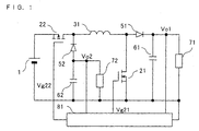
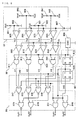
- FIG. 1 is a circuit diagram showing a configuration of a multiple output DC-DC converter in accordance with Embodiment 1 of the present invention. As shown in FIG. 1, the multiple output DC-DC converter in accordance with Embodiment 1 of the present invention is connected to an input DC power source 1 and receives an input DC voltage Ei.
- the multiple output DC-DC converter in accordance with Embodiment 1 is provided with a first main switch 21 formed of an N-channel MOSFET, a second main switch 22 formed of a P-channel MOSFET, an inductor 31, a first rectifying means 51 formed of a diode, a first smoothing means 61 formed of a capacitor, a second rectifying means 52 formed of a diode, a second smoothing means 62 formed of a capacitor, and a control circuit 81 for driving the first main switch 21 and the second main switch 22 in accordance with their respective predetermined ON and OFF periods.
- a first load 71 is connected across both the terminals of the first smoothing means 61, and a stepped-up output voltage Vo1 is output to the first load 71.
- a second load 72 is connected across both the terminals of the second smoothing means 62, and an inverted output voltage Vo2 is output to the second load 72.
- the input and output conditions in Embodiment 1 are represented by Vo1 > Ei > 0 > Vo2.
- the second main switch 22 When the second main switch 22 is ON, the first main switch 21, the inductor 31, the first rectifying means 51 and the first smoothing means 61 operate as a step-up converter.
- the second main switch 22 When the first main switch 21 is ON, the second main switch 22, the inductor 31, the second rectifying means 52 and the second smoothing means 62 operate as an inverting converter.
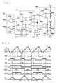
- FIG. 2 is a circuit diagram showing the configuration of the control circuit 81 in greater detail.
- a resistor 801 and a resistor 802 detect the stepped-up output voltage Vo1
- a resistor 803 and a resistor 804 detect the inverted output voltage Vo2.
- the detected voltages are compared with the reference voltage of a reference voltage source 807 by an error amplifier 805 and an error amplifier 806, respectively, whereby an error signal Ve1 for stepped-up output (stepped-up output error signal Ve1) and an error signal Ve2 for inverted output (inverted output error signal Ve2) are output, respectively.
- the resistors 801 to 804, the error amplifier 805, the error amplifier 806 and the reference voltage source 807 constitute a detection circuit 90.
- An oscillation circuit 808 outputs a triangular wave voltage Vt having a potential increasing or decreasing in a predetermined cycle, and a signal Vt1 that becomes “H” when the triangular wave voltage Vt increases and that becomes “L” when the voltage decreases.
- a comparator 809 compares the stepped-up output error signal Ve1 with the triangular wave voltage Vt.
- a comparator 810 compares the inverted output error signal Ve2 with the triangular wave voltage Vt.
- the output signals of the comparators 809 and 810 are output as a signal V1 and a signal V2 indicating ANDs with the signal Vt1 by using AND circuits 811 and 812, respectively.
- the signal V1 is a pulse signal for stepped-up output (stepped-up output pulse signal), and the signal V2 is a pulse signal for inverted output (inverted output pulse signal).
- the comparators 809 and 810 and the AND circuits 811 and 812 constitute a PWM circuit 91.
- a T flip-flop 813 serving as a frequency division circuit receives the signal Vt1 and outputs a signal Vt2.
- An OR circuit 814 receives the signal V1 and the signal Vt2 and outputs a drive signal Vg21.
- the drive signal Vg21 drives the first main switch 21 formed of an N-channel MOSFET and turns ON the first main switch 21 when the signal is "H.”
- a NOR circuit 815 receives the signal V2 and the inverted signal of the signal Vt2 and outputs a drive signal Vg22.
- the drive signal Vg22 drives the second main switch 22 formed of a P-channel MOSFET and turns ON the second main switch 22 when the signal is "L.”
- the drive signal Vg21 and the drive signal Vg22 are main switch drive signals.
- the OR circuit 814 and the NOR circuit 815 constitute a logic circuit 92.
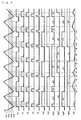
- FIG. 3 is a waveform diagram showing the above-mentioned respective signals and a current I31 flowing through the inductor 31.
- the operation of the multiple output DC-DC converter in accordance with Embodiment 1 of the present invention will be described below by using FIG. 1 to FIG. 3.
- the triangular wave signal Vt starts rising, the signal Vt1 becomes "H,” and the signal Vt2, that is, the output of the T flip-flop 813 to which the signal Vt1 is input, becomes “L.”
- the signal V1 indicating the AND of the signal Vt and the result of the comparison between the triangular wave signal Vt and the error signal Ve1 becomes "H.”
- the drive signal Vg21 that is, the AND of the signal V1 and the signal Vt2 becomes "H.” In other words, the first main switch 21 becomes ON.
- the inverted signal of the signal Vt2 is "H," and the drive signal Vg22, that is, the output of the NOR circuit 815 to which this inverted signal is input, becomes “L.”
- the second main switch 22 becomes ON.
- the input DC voltage Ei is applied to the inductor 31, whereby magnetic energy is stored.
- the triangular wave signal Vt starts rising, the signal Vt1 becomes “H” again, and the output signal Vt2 of the T flip-flop 813 becomes “H.”
- the drive signal Vg21 that is, the output of the OR circuit 814 to which the signal Vt2 is input, becomes “H.”
- the first main switch 21 becomes ON.
- the signal V2, that is, the AND of the signal Vt and the result of the comparison between the triangular wave signal Vt and the error signal Ve2 becomes "H”
- the drive signal Vg22 that is, the output of the NOR circuit 815 to which the signal V2 is input, becomes “L.”
- the second main switch 22 becomes ON.
- the input DC voltage Ei is applied to the inductor 31, whereby magnetic energy is stored.
- the drive signal Vg22 that is, the output of the NOR circuit 815 to which the signal V2 and the signal Vt2 are input, becomes “H.”
- the second main switch 22 becomes OFF.
- the drive signal Vg21 that is, the output of the OR circuit 814, is "H” since the signal Vt2, an H-level signal, is input.
- the first main switch 21 remains ON.
- the magnetic energy stored in the inductor 31 is released as a current for charging the capacitor serving as the second smoothing means 62 via the second rectifying means 52.
- this current becomes zero.
- the triangular wave voltage Vt turns from rising to lowering, and the signal Vt1 becomes "L” simultaneously.
- the error signals Ve1 and Ve2 increase or decrease so that the stepped-up output voltage Vo1 and the inverted output voltage Vo2 are stabilized to desired voltages, whereby the periods in which both the first main switch 21 and the second main switch 22 are ON are adjusted.
- the step-up converter and the inverting converter, in which the inductor 31 is shared undergo time-shared control at half the oscillation frequency of the oscillator 808, whereby the stepped-up output voltage Vo1 and the inverted output voltage Vo2 are stabilized to the desired voltages.
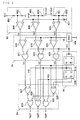
- FIG. 4 is a circuit diagram showing the configuration of a multiple output DC-DC converter in accordance with Embodiment 2 of the present invention.
- the multiple output DC-DC converter in accordance with Embodiment 2 components similar to those of the configuration of the multiple output DC-DC converter in accordance with Embodiment 1 shown in FIG. 1 are designated by the same numerals.
- Embodiment 2 differs from the configuration of the DC-DC converter in accordance with Embodiment 1 shown in FIG.
- the stepped-up output voltage Vo1 output from the first smoothing means is a first stepped-up output voltage
- a series circuit of an auxiliary switch 41 formed of an N-channel MOSFET and a third rectifying means 53 formed of a diode is provided, and that a third smoothing means 63 formed of a capacitor is provided.
- this embodiment also differs in that a second stepped-up output voltage Vo3 is added and output to a third load 73.
- Embodiment 2 in order to control the second stepped-up output voltage Vo3, functions for the purpose are additionally provided for a control circuit 82, whereby the circuit configuration shown in FIG. 5 is obtained.
- the input and output conditions in Embodiment 2 are represented by Vo1 > Vo3 > Ei > 0 > Vo2.
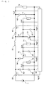
- FIG. 5 is a circuit diagram showing the configuration of the control circuit 82 in accordance with Embodiment 2 in greater detail. Referring to FIG. 5, differences from the configuration of Embodiment 1 shown in FIG. 2 will be described below.
- a detection circuit 93 in accordance with Embodiment 2 is additionally provided with, in addition to the configuration of the detection circuit 90 of FIG. 2, a resistor 821 and a resistor 822 for detecting the second stepped-up output voltage Vo3, and an error amplifier 823 for comparing the detected voltage with the reference voltage of the reference voltage source 807.
- a PWM circuit 94 in accordance with Embodiment 2 is additionally provided with, in addition to the configuration of the PWM circuit 91 of FIG.
- a comparator 824 for comparing an error signal Ve3 for stepped-up output (stepped-up output error signal Ve3), that is, the output of the error amplifier 823, with the triangular wave voltage Vt, and an AND circuit 825 for outputting a signal V3 indicating the AND of the output signal of the comparator 824 and the signal Vt1.
- a frequency division circuit 95 in accordance with Embodiment 2 is additionally provided with, in addition to the T flip-flop 813 for receiving the signal Vt1 and outputting the signal Vt2, a second T flip-flop 826 for receiving the signal Vt2.
- a logic circuit 96 in accordance with Embodiment 2 is additionally provided with, in addition to the configuration of the logic circuit 92 of FIG.
- NOR circuit 827 for receiving the signal V1 and the signal Vt2 and a NOR circuit 828 for receiving the signal V3, the inverted signal of the signal Vt2 and the inverted signal of the output Vt3 of the second T flip-flop 826.
- Embodiment 2 instead of the OR circuit 814 shown in FIG. 2, a NOR circuit 829 for outputting the drive signal Vg21 is provided; this NOR circuit 829 is configured so as to receive the output of the NOR circuit 827 and the output of the NOR circuit 828. Moreover, in Embodiment 2, instead of the NOR circuit 815 of FIG. 2, a NOR circuit 830 for outputting the drive signal Vg22 is provided; this NOR circuit 830 is configured so as to receive the signal V2, the inverted signal of the signal Vt2 and the signal Vt3.
- an AND circuit 831 for outputting a stepped-up output auxiliary switch drive signal Vg41 that is, the AND of the signal Vt2 and the signal Vt3, is provided.
- the stepped-up output auxiliary switch drive signal Vg41 turns ON/OFF the auxiliary switch 41.
- the logic circuit 96 in accordance with Embodiment 2 comprises the NOR circuits 827 to 830 and the AND circuit 831.
- FIG. 6 is a waveform diagram showing the above-mentioned respective signals and a current I32 flowing through an inductor 32.
- the operation of the multiple output DC-DC converter in accordance with Embodiment 2 of the present invention will be described below by using FIG. 4 to FIG. 6.
- the triangular wave signal Vt starts rising, the signal Vt1 becomes “H,” and the output Vt2 of the T flip-flop 813 to which the signal Vt1 is input, becomes “L.” Furthermore, the output Vt3 of the T flip-flop 826 to which the signal Vt2 is input, remains “H.”
- the drive signal Vg41 that is, the AND of the signal Vt2 and the signal Vt3, becomes “L,” whereby the auxiliary switch 41 is OFF.
- the drive signal Vg22 that is, the output of the NOR circuit 830 that includes the signal Vt3 as an input becomes “L,” whereby the second main switch 22 is ON.
- the signal V1 becomes "H,” whereby the output of the NOR circuit 827 to which the signal V1 is input becomes “L.” Furthermore, the output of the NOR circuit 828 to which the inverted signal of the signal Vt2 is input also becomes “L.” As a result, the drive signal Vg21, that is, the output of the NOR circuit 829, becomes “H.” In other words, the first main switch 21 becomes ON. At this time, the input DC voltage Ei is applied to the inductor 32, whereby magnetic energy is stored.
- the signal V2 indicating the AND of the signal Vt and the result of the comparison between the triangular wave signal Vt and the error signal Ve3 becomes "H,” and the output of the NOR circuit 830 to which the signal V2 is input, also becomes “H,” whereby the drive signal Vg22 is "L.”
- the second main switch 22 is ON.
- the drive signal Vg41 that is, the AND of the signal Vt2 and the signal Vt3, is "L”
- the auxiliary switch 41 remains OFF.
- the input DC voltage Ei is applied to the inductor 32, whereby magnetic energy is stored.
- the comparator 810 is inverted, and the signal V2 becomes "L,” whereby all the inputs of the NOR circuit 830 become “L.”
- the drive signal Vg22 that is, the output of the NOR circuit 830
- the second main switch 22 becomes OFF. Since the signal Vt2 remains “H” and the signal Vt3 remains “L,” the drive signal Vg21 remains “H” and the drive signal Vg41 remains “L.”
- the first main switch 21 is ON and the auxiliary switch 41 is OFF.
- the magnetic energy stored in the inductor 32 is released as a current for charging the capacitor serving as the second smoothing means 62 via the second rectifying means 52.
- this current I32 flowing through the inductor 32 becomes zero.
- the triangular wave voltage Vt turns from rising to lowering, and the signal Vt1 becomes "L" simultaneously at that time.
- the auxiliary switch 41 since the auxiliary switch 41 is OFF, the magnetic energy stored in the inductor 32 is released as a current for charging the capacitor serving as the first smoothing means 61 via the first rectifying means 51. Then, at time t8, the current I32 flowing through the inductor 32 becomes zero. As shown in FIG. 6, until up to time t9, the triangular wave voltage Vt turns from rising to lowering, and the signal Vt1 becomes "L" simultaneously at that time.
- the triangular wave signal Vt turns to rising, the signal Vt1 becomes “H” again, the signal Vt2 becomes “H,” and the signal Vt3 also becomes “H.”
- the drive signal Vg41 that is, the AND of the signal Vt2 and the signal Vt3, becomes “H,” whereby the auxiliary switch 41 becomes ON.
- the output of the NOR circuit 830 to which the signal Vt3 is input is "L,” the drive signal Vg22 is "L,” and the second main switch 22 also remains ON.
- the signal V3 indicating the AND of the signal Vt and the result of the comparison between the triangular wave signal Vt and the error signal Ve3 becomes "H," and the output of the NOR circuit 828 to which the signal V3 is input, becomes “L.”
- the drive signal Vg21 becomes "H.”
- the first main switch 21 becomes ON.
- the input DC voltage Ei is applied to the inductor 32, whereby magnetic energy is stored.
- the comparator 825 is inverted, and the signal V3 becomes “L,” whereby all the inputs of the NOR circuit 828 become “L” and its output becomes “H.”
- the output of the NOR circuit 829 that is, the drive signal Vg21
- the drive signal Vg22 remains “L” and the drive signal Vg41 remains “H.”
- the second main switch 22 is ON and the auxiliary switch 41 also remains ON.
- the triangular wave voltage Vt turns from rising to lowering, and the signal Vt1 becomes “L” simultaneously.
- the triangular wave signal Vt turns to rising, whereby the signal Vt1 becomes “H” again, the signal Vt2 becomes “L,” the signal Vt3 becomes “H,” and the operation after time t0 is repeated.
- Ton1 that the ON period of the first main switch 21 and the second main switch 22, corresponding to the period in which the signal V2 is "H,” just like the period between time t3 and t4, is Ton2, that the ON period of the first main switch 21 and the second main switch 22, in which the auxiliary switch 41 is ON, just like the period between time t9 and t10, is Ton3, that the output current to the first load 71 is Io1, that the output current to the second load 72 is Io2, and that the output current to the third load 73 is Io3, the relationships of the following equations (3), (4) and (5) are established.
- Vo1 Ei + (Ei ⁇ Ton1) 2 / (4L ⁇ T ⁇ Io1)
- Vo2 - (Ei ⁇ Ton2) 2 / (8L ⁇ T ⁇ Io2)
- Vo3 Ei + (Ei ⁇ Ton3) 2 / (8L ⁇ T ⁇ Io3)
- the error signals Ve1, Ve2 and Ve3 increase or decrease so that the first stepped-up output voltage Vo1, the inverted output voltage Vo2 and the second stepped-up output voltage Vo3 are stabilized to desired voltages, whereby the ON periods of the first main switch 21 and the second main switch 22 are adjusted.
- the step-up converter for supplying the first stepped-up output voltage undergoes time-shared control at 2/4 the oscillation frequency of the oscillator 808, and the other step-up converter and the inverting converter undergo time-shared control at 1/4 the oscillation frequency.
- the multiple output DC-DC converter in accordance with Embodiment 2 can stabilize the first stepped-up output voltage, the second stepped-up output voltage and the inverted output voltage to the respective desired voltages.
- Embodiment 2 provides the configuration in which the one inverter 32 is shared, whereby it is possible to obtain an excellent effect of being capable of simultaneously stabilizing the two stepped-up outputs and the single inverted output by using a smaller number of components.
- the step-up converter for supplying the first stepped-up output voltage undergoes time-shared control at 2/4 the oscillation frequency of the oscillator 808; however, 2/4 the oscillation frequency may be assigned to the step-up converter for supplying the second stepped-up output voltage, and the other converters may undergo time-shared control at 1/4 the oscillation frequency.
- the converter having larger output power should be selected; the selection is possible as desired depending on the logic circuit constituting the control circuit.
- FIG. 7 is a circuit diagram showing the configuration of a multiple output DC-DC converter in accordance with Embodiment 3 of the present invention.
- Embodiment 3 components similar to those of the configuration of the multiple output DC-DC converter in accordance with Embodiment 2 described above and shown in FIG. 4 are designated by the same numerals.
- the multiple output DC-DC converter in accordance with Embodiment 3 differs from the configuration of Embodiment 2 shown in FIG.
- Embodiment 4 in that when it is assumed that the inverted output voltage to be supplied to the load 72 is a first inverted output voltage Vo2, a series circuit of a second auxiliary switch 42 formed of a P-channel MOSFET and a fourth rectifying means 54 formed of a diode is provided, that a fourth smoothing means 64 formed of a capacitor is provided, and that a configuration for outputting a second inverted output voltage Vo4 to a fourth load 74 is added.
- functions for the purpose are additionally provided for a control circuit 83, whereby the configuration shown in FIG. 8 is obtained.
- the input and output conditions in Embodiment 3 are represented by Vo1 > Vo3 > Ei > 0 > Vo4 > Vo2.
- FIG. 8 is a circuit diagram showing the configuration of the control circuit 83 in greater detail. Referring to FIG. 8, differences from the configuration of Embodiment 2 shown in FIG. 5 will be described below.
- a detection circuit 97 in accordance with Embodiment 3 is additionally provided with, in addition to the configuration of the detection circuit 93 shown in FIG. 5, a resistor 841 and a resistor 842 for detecting the second inverted output voltage Vo4, and an error amplifier 843 for comparing the detected voltage with the reference voltage of the reference voltage source 807.
- a PWM circuit 98 in accordance with Embodiment 3 is additionally provided with, in addition to the configuration of the PWM circuit 94 shown in FIG.
- a comparator 844 for comparing an error signal Ve4, that is, the output of the error amplifier 824, with the triangular wave voltage Vt, an AND circuit 845 for outputting a signal V4 indicating the AND of the output signal of this comparator 844 and the signal Vt1, an OR circuit 846 to which the signal Vt2 and the signal Vt3 are input, and a NOR circuit 848 to which the signal V4, the signal Vt2 and the signal Vt3 are input.
- a logic circuit 99 in accordance with Embodiment 3 is provided with, instead of the NOR circuit 827 in the logic circuit 96 shown in FIG.
- NOR circuit 847 to which the signal V1, the signal Vt2 and the inverted signal of the signal Vt3 are input and from which the drive signal Vg21 is output to the NOR circuit 829.
- the NOR circuit 829 for outputting the drive signal Vg21 is configured so as to receive the output of the NOR circuit 847 and the output of the NOR circuit 828.
- the output of the NOR circuit 830 is input to the OR circuit 849 together with the output of the NOR circuit 848, and the OR circuit 849 is configured to output the drive signal Vg22.
- the OR circuit 846 is provided; this OR circuit 846 outputs a drive signal Vg42 thereby to turn ON/OFF the second auxiliary switch 42.
- the logic circuit 99 comprises the NOR circuits 828 to 830, 847 and 848, the AND circuit 831 and the OR circuits 846 and 849.
- FIG. 9 is a waveform diagram showing the above-mentioned respective signals and a current I33 flowing through an inductor 33.
- the operation of the multiple output DC-DC converter in accordance with Embodiment 3 of the present invention will be described below by using FIG. 7 to FIG. 9.
- the triangular wave signal Vt starts rising; the signal Vt1 becomes “H,” and, the output Vt2 of the T flip-flop 813 to which the signal Vt1 is input becomes “L.” Furthermore, the output Vt3 of the T flip-flop 826 to which the signal Vt2 is input remains “H.” Hence, the drive signal Vg41 becomes “L,” whereby the auxiliary switch 41 is OFF. The second drive signal Vg42 becomes “H,” whereby the second main switch 42 is OFF. At time t0, the drive signal Vg22, that is, the output of the OR circuit 849, is "L,” whereby the second main switch 22 remains ON.
- the signal V2 indicating the AND of the signal Vt1 and the result of the comparison between the triangular wave signal Vt and the error signal Ve2 becomes "H," and the output of the NOR circuit 830 also becomes “H.”
- the drive signal Vg22 output from the OR circuit 849 becomes "L.”
- the second main switch 22 is ON at this time.
- the drive signal Vg41 remains “L” and the drive signal Vg42 remains “H,” whereby the auxiliary switch 41 and the second auxiliary switch 42 remain OFF.
- the input DC voltage Ei is applied to the inductor 33, whereby magnetic energy is stored.
- the comparator 810 is inverted, and the signal V2 becomes “L,” whereby all the inputs of the NOR circuit 830 become “L,” and the output of the OR circuit 849 to which the output of the NOR circuit being “H” is input becomes “H.”
- the drive signal Vg22 becomes “H,” whereby the second main switch 22 becomes OFF. Since the signal Vt2 remains “H” and the signal Vt3 remains “L,” the drive signal Vg21 remains “H,” the drive signal Vg41 remains “L,” and the drive signal Vg42 remains “H.”
- the first main switch 21 is ON, and the auxiliary switch 41 and the second auxiliary switch 42 are OFF.
- the magnetic energy stored in the inductor 33 is released as a current for charging the capacitor serving as the second smoothing means 62 via the second rectifying means 52. Then, at time t5, the current I33 flowing through the inductor 33 becomes zero. As shown in FIG. 9, until up to time t6, the triangular wave voltage Vt turns from rising to lowering, and the signal Vt1 becomes "L" simultaneously at that time.
- the triangular wave signal Vt turns to rising, the signal Vt1 becomes “H” again, the signal Vt2 becomes “L,” and the signal Vt3 remains “L.”
- the drive signal Vg41 is “L,” and the auxiliary switch 41 remains OFF.
- the drive signal Vg42 becomes “L,” whereby the second auxiliary switch 42 becomes ON.
- both the outputs of the NOR circuit 847 and the NOR circuit 828 become “L,” whereby the drive signal Vg21 is “H,” and the first main switch 21 is ON.
- the output from the NOR circuit 830 to the OR circuit 849 is “L,” and the output from the NOR circuit 848 to the OR circuit 849 becomes “L” since the signal V4 is "H.”
- the output signal of the OR circuit 849 becomes “L.”
- the drive signal Vg22 becomes "L” the second main switch 22 becomes ON.
- the input DC voltage Ei is applied to the inductor 33, whereby magnetic energy is stored.
- the comparator 844 is inverted, and the signal V4 becomes "L,” whereby the output of the NOR circuit 848 becomes “H.”
- the drive circuit Vg22, the output of the OR circuit 849 becomes "H,” and the second main switch 22 becomes OFF.
- the drive signal Vg21 remains “H”
- the drive signal Vg41 remains “L”
- the drive signal Vg42 remains “L.”
- the first main switch 21 is ON
- the auxiliary switch 41 is OFF
- the second auxiliary switch 42 is ON.
- the magnetic energy stored in the inductor 33 is released as a current for charging the capacitor serving as the fourth smoothing means 64 via the fourth rectifying means 54.
- the current I33 flowing through the inductor 33 becomes zero.
- the triangular wave voltage Vt turns from rising to lowering, and the signal Vt1 becomes "L" simultaneously at that time.
- the signal V3 indicating the AND of the signal Vt and the result of the comparison between the triangular wave signal Vt and the error signal Ve3 becomes "H," and the output of the NOR circuit 828 to which the signal V3 is input, becomes “L.”
- the drive signal Vg21 becomes "H.”
- the first main switch 21 becomes ON.
- the input DC voltage Ei is applied to the inductor 33, whereby magnetic energy is stored.
- the comparator 825 is inverted, and the signal V3 becomes “L,” whereby all the inputs of the NOR circuit 828 become “L.” As a result, the output of the NOR circuit 828 becomes “H.”
- the output of the NOR circuit 829 that is, the drive signal Vg21
- the first main switch 21 becomes OFF.
- the drive signal Vg22 remains “L”
- the drive signal Vg41 remains “H”
- the drive signal Vg42 remains “H.”
- the second main switch 22 and the auxiliary switch 41 remain ON, and the second auxiliary switch 42 remains OFF.
- the magnetic energy stored in the inductor 33 is released as a current for charging the capacitor serving as the third smoothing means 63 via the third rectifying means 53. Then, at time t11, the current 133 flowing through the inductor 33 becomes zero. As shown in FIG. 9, until up to time t12, the triangular wave voltage Vt turns from rising to lowering, and the signal Vt1 becomes "L" simultaneously at that time.
- the triangular wave signal Vt turns to rising, whereby the signal Vt1 becomes “H” again, the signal Vt2 becomes “L,” the signal Vt3 becomes “H,” and the above-mentioned operation after time t0 is repeated.
- Ton1 that the ON period of the first main switch 21 and the second main switch 22, corresponding to the period in which the signal V2 is "H,” just like the period between time t3 and t4, is Ton2, that the ON period of the first main switch 21 and the second main switch 22, in which the second auxiliary switch 42 is ON, just like the period between time t6 and t7, is Ton4, that the ON period of the first main switch 21 and the second main switch 22, in which the auxiliary switch 41 is ON, just like the period between time t9 and t10, is Ton3, that the output current to the first load 71 is Io1, that the output current to the second load 72 is Io2, that the output current to the third load 73 is Io3, and that the output current to the fourth load 74 is Io4, the relationships of the following equations (6), (7), (8) and (9) are established.
- Vo1 Ei + (Ei ⁇ Ton1) 2 /(8L ⁇ T ⁇ Io1)
- Vo2 - (Ei ⁇ Ton2) 2 /(8L ⁇ T ⁇ Io2)
- Vo3 Ei + (Ei ⁇ Ton3) 2 /(8L ⁇ T ⁇ Io3)
- Vo4 -(Ei ⁇ Ton4) 2 /(8L ⁇ T ⁇ Io4)
- the error signals Ve1, Ve2, Ve3 and Ve4 increase or decrease so that the first stepped-up output voltage Vo1, the first inverted output voltage Vo2, the second stepped-up output voltage Vo3 and the second inverted output voltage Vo4 are stabilized to respective desired voltages, whereby the ON periods of the first main switch 21 and the second main switch 22 are adjusted.
- the two step-up converters and the two inverting converters, in which the inductor 33 is shared undergo time-shared control at 1/4 the oscillation frequency of the oscillator 808, whereby the output voltages are stabilized to the respective desired voltages.
- Embodiment 3 it is possible to obtain an excellent effect of being capable of stabilizing the two stepped-up outputs and the two inverted outputs by using a smaller number of components attained by sharing the single inductor 33.
- time-shared control at 1/4 the oscillation frequency of the oscillator 808 is assigned to the two step-up converters and the two inverting converters; however, the multiple output DC-DC converter in accordance with the present invention is not limited to have this configuration.
- the multiple output DC-DC converter in accordance with the present invention can have a configuration formed of one step-up converter and two inverting converters as shown in a circuit diagram in FIG. 10, for example, although explanations are omitted.
- the multiple output DC-DC converter in accordance with the present invention can have a configuration formed of three step-up converters and one inverting converter as shown in another circuit diagram in FIG. 11.
- the multiple output DC-DC converter in accordance with the present invention can have a configuration formed of one step-up converter and three inverting converters as shown in still another circuit diagram in FIG. 12.
- time-shared control can be carried out at (-N)th power of 2 times the oscillation frequency of the oscillator 808 by using N stages of T flip-flops serving as frequency division circuits.
- the present invention has the following effects.
- the multiple output DC-DC converter in accordance with the present invention requires only one inductor in order to supply controlled step-up or inverted outputs to a plurality of loads, whereby it can be configured by using a smaller number of components.
- the power source circuit for the liquid crystal panel of the prior-art portable apparatus comprised two step-up converters and one inverting-type switched capacitor and requires eight semiconductor switches including diodes, two inductors and four capacitors.
- the output voltage from the inverting-type switched capacitor was unable to be controlled.
- this power source circuit can comprise six semiconductor switches, one inductor and three capacitors.
- each output can be controlled by adjusting the ON/OFF period ratio of the main switch circuit corresponding thereto.
- the present invention does not require series regulators or switched capacitors, thereby having an excellent effect of being capable of obtaining highly efficient features inherent in a switching converter.
- the multiple output DC-DC converter in accordance with the present invention is used as a power source for driving electronic components installed in various electronic apparatuses, such as portable apparatuses, requiring a plurality of power source voltages; the present invention is thus highly versatile.
Landscapes
- Engineering & Computer Science (AREA)
- Power Engineering (AREA)
- Dc-Dc Converters (AREA)
Abstract
In order to supply controlled DC voltages to
a plurality of loads at high efficiency by using
smaller number of components, a multiple output DC-DC
converter in accordance with the present invention
comprises a first main switch 21, one terminal of
which is connected to the negative electrode of an
input DC power source 1, a first rectifying means 51
and a first smoothing means 61 connected to the other
terminal of the first main switch 21, a second main
switch 22, one terminal of which is connected to the
positive terminal of the input DC power source 1, a
second rectifying means 52 and a second smoothing
means 62 connected to the other terminal of the second
main switch 22, an inductor 31 connected between the
other terminal of the first main switch 21 and the
other terminal of the second main switch 22, and a
control circuit 81 for driving the respective switches
at predetermined ON/OFF period ratios.
Description
The present invention relates to a multiple
output DC-DC converter, for use in a power source for
driving a liquid crystal panel or the like installed
in a portable apparatus, for example, that receives a
DC voltage from a battery or the like and supplies
controlled DC voltages including negative voltages to
a plurality of loads.
As a prior art relating to a multiple output
DC-DC converter that receives a DC voltage and
supplies controlled DC voltages to a plurality of
loads, a configuration shown in FIG. 13 is available.
The prior-art multiple output DC-DC converter shown in
FIG. 13 is a power source for driving a liquid crystal
panel installed in a portable apparatus. In this
multiple output DC-DC converter, an input DC voltage
Ei = 2.5 to 3.3 V is supplied from a battery serving
as an input power source 1; a first output voltage
Vout1 = 3.5 V is output as a source drive voltage; and
a second output voltage Vout2 = 13.5 V and a third
output voltage Vout3 = -13.5 V are output as positive
and negative gate drive voltages. A first converter
100 is provided with a first main switch 102 formed of
an N-channel MOSFET, a first inductor 103, a first
diode 105 for output (first output diode 105) and a
first capacitor 106 for output (first output capacitor
106). A step-up converter for outputting the first
output voltage Vout1 from the first output capacitor
106 to a first load 107 is formed by the first
converter 100. A first control circuit 108 adjusts
the ON/OFF ratio of the first main switch 102 to
control the first output voltage Vout1. A second
converter 200 is provided with a second main switch
202 formed of an N-channel MOSFET, a second inductor
203, a second diode 205 for output (second output
diode 205) and a second capacitor 206 for output
(second output capacitor 206). A step-up converter
for outputting the second output voltage Vout2 from
the second output capacitor 206 to a second load 207
is formed by this second converter 200. A second
control circuit 208 adjusts the ON/OFF ratio of the
second main switch 202 to control the second output
voltage Vout2. A third converter 300 receives the
second output voltage Vout2 and is provided with a
first switch 301, a second switch 302, a capacitor 303,
a first diode 304, a second diode 305 and a third
capacitor 306 for output (third output capacitor 306).
An inverting-type switched capacitor for outputting
the third output voltage Vout3 from the third output
capacitor 306 to a third load 307 is formed by this
third converter 300. A third control circuit 308
carries out control so as to alternately turn ON and
OFF the first switch 301 and the second switch 302.
The operation of the prior-art multiple
output DC-DC converter shown in FIG. 13 will be
described below briefly. First, in the first
converter 100, when the first main switch 102 is ON,
the input DC voltage Ei is applied to the first
inductor 103. At this time, current flows through the
first inductor 103 and magnetic energy is stored.
Then, when the first main switch 102 becomes OFF, the
magnetic energy stored in the first inductor 103 is
released as a current for charging the first output
capacitor 106 via the first output diode 105. When it
is assumed that the first main switch 102 turns ON/OFF
in a constant cycle, the energy being output every
cycle via the first inductor 103 becomes larger as the
ON period of the first main switch 102 is longer.
Accordingly, the first output voltage Vout1 becomes
higher as the ON period of the first main switch 102
is longer. In other words, the first control circuit
108 adjusts the ON/OFF period ratio of the first main
switch 102, whereby the first output voltage Vout1 is
controlled. Similarly, in the second converter 200,
the control circuit 208 adjusts the ON/OFF period
ratio of the second main switch 202, whereby the
magnetic energy stored in the second inductor 203 is
released as a current for charging the second output
capacitor 206 via the second output diode 205. The
release amount of this magnetic energy is adjusted,
whereby the second output voltage Vout2 is controlled.
In the third converter 300, when the first
switch 301 is ON, the second output voltage Vout
charges the capacitor 303 via the second diode 305.
When the second switch 302 is ON, the energy of the
capacitor 303 charges the third output capacitor 306
via the first diode 304, whereby the third output
voltage Vout3, obtained by inverting the second output
voltage Vout2 to its negative side, is output.
In the above-mentioned configuration, in
order to output three kinds of different voltages,
three converters are required. However, in portable
apparatuses, the number of components is requested to
be made smaller, even a single component, in order to
attain miniaturization and weight reduction. As means
for controlling a plurality of outputs by using
smaller number of components, an art described in
Japanese Patent Examined Publication No. Hei 7-40785
is available, for example. FIG. 14 is a circuit
diagram of a step-up converter having three outputs
disclosed in FIG. 1 of Japanese Patent Examined
Publication No. Hei 7-40785. in FIG. 14, magnetic
energy from an input DC power source V11 is stored
while a switch S1 is in contact with a contact 1. The
magnetic energy is released to the output side while
the switch S1 is in contact with a contact 2. At that
time, the magnetic energy is distributed to each
output by a switch S2. The invention disclosed in
Japanese Patent Examined Publication No. Hei 7-40785
indicates a method for stabilizing the output of each
output by controlling the ON period in which the
switch S2 is in contact with each contact and for
controlling the switch S1 so that electricity is
supplied to all loads just sufficiently.
Japanese Patent Examined Publication No. Hei
7-40785 discloses a system wherein the contacts of the
switch S2 are switched by time-sharing the period in
which the switch S1 is in contact with the contact 2
(the OFF period of the main switch). Although being
different in circuit configuration from this prior art,
an invention relating to a different control method
configured on the basis of a similar technical concept
is known. For example, the specification of U.S.
Patent No. 5,400,239 discloses an insulation-type
flyback converter having N outputs. In this
insulation-type flyback converter, N rectifying and
smoothing circuits are connected to one output winding
of a transformer via a switch corresponding to the
switch S2. Furthermore, the switching frequency of
the main switch is divided by N and assigned to the
control of each output. In other words, when this
insulation-type flyback converter is replaced with the
configuration shown in FIG. 14, the switch S2 is
switched in accordance with a 1/N switching frequency,
and the ON period of the switch S1 is adjusted every
switching cycle, whereby each output voltage is
controlled.
In addition, the specification of U.S.
Patent No. 5,751,139 discloses a multiple output non-insulation-type
DC-DC converter provided with one
inductor. In this non-insulation-type DC-DC converter,
priority is given to outputs desired to be stabilized.
When the configuration of this non-insulation-type DC-DC
converter is replaced with the configuration shown
in FIG. 14, the switch S2 selects outputs in
accordance with order of priority and supplies
electricity; when the voltage of a selected output
reaches its upper limit threshold value, switching is
carried out to select the output having the next order
of priority.
As described above, in the prior-art
apparatuses, the output of a single DC-DC converter is
time-shared so as to be supplied to a plurality of
outputs, and a main switch and an output selection
switch are controlled to stabilize each output. When
this kind of technology is applied to the prior-art
multiple output converter shown in FIG. 13, it is
necessary to use an output selection switch
corresponding to the switch S2 (FIG. 14). However, in
the first converter 100 and the second converter 200,
the first main switch 102 can be used as the second
main switch 202, and the first inductor 103 can be
used as the second inductor 203, whereby one inductor,
being large in volume among the components, can be
eliminated.
As described above, in order to control the
three outputs, that is, the first to third output
voltages, the prior-art multiple output DC-DC
converter comprises two step-up converters and one
inverting-type switched capacitor. However, in
portable apparatuses desired for miniaturization and
weight reduction, in particular, the number of
components is requested to be made smaller. In the
prior-art technology, in order to control the
plurality of outputs by using smaller number of
components, it is possible to reduce one inductor by
integrating the two step-up converters into one.
However, in order to generate a negative output
voltage, the inverting-type switched capacitor shown
in FIG. 13 is required. It is difficult to finely
adjust the output voltage by using this inverting-type
switched capacitor. Furthermore, since the capacitor
charging and discharging currents are surge currents,
problems due to switching noise and switching loss are
caused. It is considered to install an inverting
converter as a method for obtaining any given negative
output voltage; however, an inductor becomes necessary
instead of the capacitor used for the inverting-type
switched capacitor. Since this kind of inductor is
large in volume among the components of the converter,
apparatus miniaturization and weight reduction are
obstructed.
The present invention is intended to provide
a single DC-DC converter capable of outputting a
plurality of voltages stepped up from an input voltage
and having the same polarity as that of the input
voltage or having the opposite polarity, in other
words, a multiple output DC-DC converter capable of
controlling a plurality of outputs by using one
inductor. The present invention provides a multiple
output DC-DC converter capable of reducing the number
of components and miniaturizing the entire size of the
circuit.
In order to attain the above-mentioned
objects, the multiple output DC-DC converter in
accordance with the present invention comprises:
Furthermore, in the multiple output DC-DC
converter in accordance with the present invention,
the above-mentioned main switch comprises:
A multiple output DC-DC converter in
accordance with another aspect of the present
invention comprises:
A multiple output DC-DC converter in
accordance with still another aspect of the present
invention comprises:
While the novel features of the invention
are set forth particularly in the appended claims, the
invention, both as to organization and content, will
be better understood and appreciated, along with other
objects and features thereof, from the following
detailed description taken in conjunction with the
drawings.
It will be recognized that some or all of
the drawings are schematic representations for
purposes of illustration and do not necessarily depict
the actual relative sizes or locations of the elements
shown.
Preferred embodiments of a multiple output
DC-DC converter in accordance with the present
invention will be described below referring to the
accompanying drawings.
FIG. 1 is a circuit diagram showing a
configuration of a multiple output DC-DC converter in
accordance with Embodiment 1 of the present invention.
As shown in FIG. 1, the multiple output DC-DC
converter in accordance with Embodiment 1 of the
present invention is connected to an input DC power
source 1 and receives an input DC voltage Ei. The
multiple output DC-DC converter in accordance with
Embodiment 1 is provided with a first main switch 21
formed of an N-channel MOSFET, a second main switch 22
formed of a P-channel MOSFET, an inductor 31, a first
rectifying means 51 formed of a diode, a first
smoothing means 61 formed of a capacitor, a second
rectifying means 52 formed of a diode, a second
smoothing means 62 formed of a capacitor, and a
control circuit 81 for driving the first main switch
21 and the second main switch 22 in accordance with
their respective predetermined ON and OFF periods. A
first load 71 is connected across both the terminals
of the first smoothing means 61, and a stepped-up
output voltage Vo1 is output to the first load 71. A
second load 72 is connected across both the terminals
of the second smoothing means 62, and an inverted
output voltage Vo2 is output to the second load 72.
The input and output conditions in Embodiment 1 are
represented by Vo1 > Ei > 0 > Vo2. When the second
main switch 22 is ON, the first main switch 21, the
inductor 31, the first rectifying means 51 and the
first smoothing means 61 operate as a step-up
converter. On the other hand, when the first main
switch 21 is ON, the second main switch 22, the
inductor 31, the second rectifying means 52 and the
second smoothing means 62 operate as an inverting
converter.
FIG. 2 is a circuit diagram showing the
configuration of the control circuit 81 in greater
detail. In FIG. 2, a resistor 801 and a resistor 802
detect the stepped-up output voltage Vo1, and a
resistor 803 and a resistor 804 detect the inverted
output voltage Vo2. The detected voltages are
compared with the reference voltage of a reference
voltage source 807 by an error amplifier 805 and an
error amplifier 806, respectively, whereby an error
signal Ve1 for stepped-up output (stepped-up output
error signal Ve1) and an error signal Ve2 for inverted
output (inverted output error signal Ve2) are output,
respectively. The resistors 801 to 804, the error
amplifier 805, the error amplifier 806 and the
reference voltage source 807 constitute a detection
circuit 90. An oscillation circuit 808 outputs a
triangular wave voltage Vt having a potential
increasing or decreasing in a predetermined cycle, and
a signal Vt1 that becomes "H" when the triangular wave
voltage Vt increases and that becomes "L" when the
voltage decreases. A comparator 809 compares the
stepped-up output error signal Ve1 with the triangular
wave voltage Vt. A comparator 810 compares the
inverted output error signal Ve2 with the triangular
wave voltage Vt. The output signals of the
comparators 809 and 810 are output as a signal V1 and
a signal V2 indicating ANDs with the signal Vt1 by
using AND circuits 811 and 812, respectively. The
signal V1 is a pulse signal for stepped-up output
(stepped-up output pulse signal), and the signal V2 is
a pulse signal for inverted output (inverted output
pulse signal). The comparators 809 and 810 and the
AND circuits 811 and 812 constitute a PWM circuit 91.
A T flip-flop 813 serving as a frequency division
circuit receives the signal Vt1 and outputs a signal
Vt2. An OR circuit 814 receives the signal V1 and the
signal Vt2 and outputs a drive signal Vg21. The drive
signal Vg21 drives the first main switch 21 formed of
an N-channel MOSFET and turns ON the first main switch
21 when the signal is "H." A NOR circuit 815 receives
the signal V2 and the inverted signal of the signal
Vt2 and outputs a drive signal Vg22. The drive signal
Vg22 drives the second main switch 22 formed of a P-channel
MOSFET and turns ON the second main switch 22
when the signal is "L." In Embodiment 1, the drive
signal Vg21 and the drive signal Vg22 are main switch
drive signals. The OR circuit 814 and the NOR circuit
815 constitute a logic circuit 92.
FIG. 3 is a waveform diagram showing the
above-mentioned respective signals and a current I31
flowing through the inductor 31. The operation of the
multiple output DC-DC converter in accordance with
Embodiment 1 of the present invention will be
described below by using FIG. 1 to FIG. 3.
At time t0 of FIG. 3, the triangular wave
signal Vt starts rising, the signal Vt1 becomes "H,"
and the signal Vt2, that is, the output of the T flip-flop
813 to which the signal Vt1 is input, becomes
"L." On the other hand, the signal V1 indicating the
AND of the signal Vt and the result of the comparison
between the triangular wave signal Vt and the error
signal Ve1 becomes "H." In addition, the drive signal
Vg21, that is, the AND of the signal V1 and the signal
Vt2 becomes "H." In other words, the first main
switch 21 becomes ON. On the other hand, the inverted
signal of the signal Vt2 is "H," and the drive signal
Vg22, that is, the output of the NOR circuit 815 to
which this inverted signal is input, becomes "L." In
other words, the second main switch 22 becomes ON. At
this time, the input DC voltage Ei is applied to the
inductor 31, whereby magnetic energy is stored.
When the comparator 809 is inverted and the
signal V1 becomes "L" at time t1, since the signal Vt2
is "L," the drive signal Vg21 become "L." As a result,
the first main switch 21 becomes OFF. On the other
hand, since the drive signal Vg22 remains "L," the
second main switch 22 is ON. At this time, the
magnetic energy stored in the inductor 31 is released
as a current for charging the capacitor serving as the
first smoothing means 61 from the input DC voltage
source 1 via the first rectifying means 51. Then, at
time t2, this current becomes zero. On the other hand,
the triangular wave voltage Vt turns from rising to
lowering, and the signal Vt1 becomes "L"
simultaneously.
Next, at time t3, the triangular wave signal
Vt starts rising, the signal Vt1 becomes "H" again,
and the output signal Vt2 of the T flip-flop 813
becomes "H." Hence, the drive signal Vg21, that is,
the output of the OR circuit 814 to which the signal
Vt2 is input, becomes "H." In other words, the first
main switch 21 becomes ON. In addition, the signal V2,
that is, the AND of the signal Vt and the result of
the comparison between the triangular wave signal Vt
and the error signal Ve2 becomes "H," and the drive
signal Vg22, that is, the output of the NOR circuit
815 to which the signal V2 is input, becomes "L." In
other words, the second main switch 22 becomes ON. At
this time, the input DC voltage Ei is applied to the
inductor 31, whereby magnetic energy is stored.
When the comparator 810 is inverted and the
signal V2 becomes "L" at time t4, since the inverted
signal of the signal Vt2 is "L," the drive signal Vg22,
that is, the output of the NOR circuit 815 to which
the signal V2 and the signal Vt2 are input, becomes
"H." In other words, the second main switch 22
becomes OFF. In addition, the drive signal Vg21, that
is, the output of the OR circuit 814, is "H" since the
signal Vt2, an H-level signal, is input. At this time,
the first main switch 21 remains ON. At this time,
the magnetic energy stored in the inductor 31 is
released as a current for charging the capacitor
serving as the second smoothing means 62 via the
second rectifying means 52. Then, at time t5, this
current becomes zero. On the other hand, the
triangular wave voltage Vt turns from rising to
lowering, and the signal Vt1 becomes "L"
simultaneously.
At time t6, the triangular wave signal Vt
turns to rising, whereby the signal Vt1 becomes "H"
again, the signal Vt2 becomes "L," and the operation
after time t0 is repeated.
When it is assumed that the inductance of
the inductor 31 is L, that the oscillation cycle of
the oscillator 808 is T, that the period between time
t0 and t1 in which both the first main switch 21 and
the second main switch 22 are ON is Ton1, that the
period between time t3 and t4 is Ton2 similarly, that
the output current to the first load 71 is Io1, and
that the output current to the second load 72 is Io2,
the relationships of the following equations (1) and
(2) are established.
Vo1 = Ei + (Ei · Ton1)2 /(4L · T · Io1)
Vo2 = - (Ei · Ton2)2 / (4L · T · Io2)
The error signals Ve1 and Ve2 increase or
decrease so that the stepped-up output voltage Vo1 and
the inverted output voltage Vo2 are stabilized to
desired voltages, whereby the periods in which both
the first main switch 21 and the second main switch 22
are ON are adjusted. In other words, the step-up
converter and the inverting converter, in which the
inductor 31 is shared, undergo time-shared control at
half the oscillation frequency of the oscillator 808,
whereby the stepped-up output voltage Vo1 and the
inverted output voltage Vo2 are stabilized to the
desired voltages.
As described above, with the multiple output
DC-DC converter in accordance with Embodiment 1, it is
possible to obtain an effect of being capable of
simultaneously stabilizing the stepped-up output and
the inverted output by using a smaller number of
components attained by sharing the single inductor 31.
FIG. 4 is a circuit diagram showing the
configuration of a multiple output DC-DC converter in
accordance with Embodiment 2 of the present invention.
In the multiple output DC-DC converter in accordance
with Embodiment 2, components similar to those of the
configuration of the multiple output DC-DC converter
in accordance with Embodiment 1 shown in FIG. 1 are
designated by the same numerals. Embodiment 2 differs
from the configuration of the DC-DC converter in
accordance with Embodiment 1 shown in FIG. 1 in that
the stepped-up output voltage Vo1 output from the
first smoothing means is a first stepped-up output
voltage, that a series circuit of an auxiliary switch
41 formed of an N-channel MOSFET and a third
rectifying means 53 formed of a diode is provided, and
that a third smoothing means 63 formed of a capacitor
is provided. In addition, this embodiment also
differs in that a second stepped-up output voltage Vo3
is added and output to a third load 73.
In Embodiment 2, in order to control the
second stepped-up output voltage Vo3, functions for
the purpose are additionally provided for a control
circuit 82, whereby the circuit configuration shown in
FIG. 5 is obtained. The input and output conditions
in Embodiment 2 are represented by Vo1 > Vo3 > Ei > 0
> Vo2.
FIG. 5 is a circuit diagram showing the
configuration of the control circuit 82 in accordance
with Embodiment 2 in greater detail. Referring to FIG.
5, differences from the configuration of Embodiment 1
shown in FIG. 2 will be described below.
As shown in FIG. 5, a detection circuit 93
in accordance with Embodiment 2 is additionally
provided with, in addition to the configuration of the
detection circuit 90 of FIG. 2, a resistor 821 and a
resistor 822 for detecting the second stepped-up
output voltage Vo3, and an error amplifier 823 for
comparing the detected voltage with the reference
voltage of the reference voltage source 807. A PWM
circuit 94 in accordance with Embodiment 2 is
additionally provided with, in addition to the
configuration of the PWM circuit 91 of FIG. 2, a
comparator 824 for comparing an error signal Ve3 for
stepped-up output (stepped-up output error signal Ve3),
that is, the output of the error amplifier 823, with
the triangular wave voltage Vt, and an AND circuit 825
for outputting a signal V3 indicating the AND of the
output signal of the comparator 824 and the signal Vt1.
A frequency division circuit 95 in accordance with
Embodiment 2 is additionally provided with, in
addition to the T flip-flop 813 for receiving the
signal Vt1 and outputting the signal Vt2, a second T
flip-flop 826 for receiving the signal Vt2. A logic
circuit 96 in accordance with Embodiment 2 is
additionally provided with, in addition to the
configuration of the logic circuit 92 of FIG. 2, a NOR
circuit 827 for receiving the signal V1 and the signal
Vt2 and a NOR circuit 828 for receiving the signal V3,
the inverted signal of the signal Vt2 and the inverted
signal of the output Vt3 of the second T flip-flop 826.
Furthermore, in Embodiment 2, instead of the
OR circuit 814 shown in FIG. 2, a NOR circuit 829 for
outputting the drive signal Vg21 is provided; this NOR
circuit 829 is configured so as to receive the output
of the NOR circuit 827 and the output of the NOR
circuit 828. Moreover, in Embodiment 2, instead of
the NOR circuit 815 of FIG. 2, a NOR circuit 830 for
outputting the drive signal Vg22 is provided; this NOR
circuit 830 is configured so as to receive the signal
V2, the inverted signal of the signal Vt2 and the
signal Vt3. Still further, in Embodiment 2, an AND
circuit 831 for outputting a stepped-up output
auxiliary switch drive signal Vg41, that is, the AND
of the signal Vt2 and the signal Vt3, is provided.
The stepped-up output auxiliary switch drive signal
Vg41 turns ON/OFF the auxiliary switch 41. The logic
circuit 96 in accordance with Embodiment 2 comprises
the NOR circuits 827 to 830 and the AND circuit 831.
FIG. 6 is a waveform diagram showing the
above-mentioned respective signals and a current I32
flowing through an inductor 32. The operation of the
multiple output DC-DC converter in accordance with
Embodiment 2 of the present invention will be
described below by using FIG. 4 to FIG. 6.
At time t0 of FIG. 6, the triangular wave
signal Vt starts rising, the signal Vt1 becomes "H,"
and the output Vt2 of the T flip-flop 813 to which the
signal Vt1 is input, becomes "L." Furthermore, the
output Vt3 of the T flip-flop 826 to which the signal
Vt2 is input, remains "H." Hence, the drive signal
Vg41, that is, the AND of the signal Vt2 and the
signal Vt3, becomes "L," whereby the auxiliary switch
41 is OFF. In addition, the drive signal Vg22, that
is, the output of the NOR circuit 830 that includes
the signal Vt3 as an input becomes "L," whereby the
second main switch 22 is ON. On the one hand, the
signal V1 becomes "H," whereby the output of the NOR
circuit 827 to which the signal V1 is input becomes
"L." Furthermore, the output of the NOR circuit 828
to which the inverted signal of the signal Vt2 is
input also becomes "L." As a result, the drive signal
Vg21, that is, the output of the NOR circuit 829,
becomes "H." In other words, the first main switch 21
becomes ON. At this time, the input DC voltage Ei is
applied to the inductor 32, whereby magnetic energy is
stored.
When the signal V1 becomes "L" at time t1,
since the signal Vt2 is "L," the output of the NOR
circuit 827 becomes "H." Hence, the output of the NOR
circuit 829 to which the output of the NOR circuit 827
is input, that is, the drive signal Vg21, becomes "L."
As a result, the first main switch 21 becomes OFF. On
the other hand, since the signal Vt2 remains "L" and
the signal Vt3 remains "H," the drive signal Vg22
remains "L" and the drive signal Vg41 remains "L."
The second main switch 22 is ON and the auxiliary
switch 41 is OFF. At this time, since the auxiliary
switch 41 is OFF, the magnetic energy stored in the
inductor 32 is released as a current for charging the
capacitor serving as the first smoothing means 61 via
the first rectifying means 51. Then, at time t2, this
current I32 flowing through the inductor 32 becomes
zero. As shown in FIG. 6, until up to time t3, the
triangular wave voltage Vt turns from rising to
lowering, and the signal Vt1 becomes "L"
simultaneously at that time.
At time t3, the triangular wave signal Vt
turns to rising, the signal Vt1 becomes "H" again, the
signal Vt2 becomes "H," and the signal Vt3 becomes
"L." Hence, the output of the NOR circuit 827 to
which the signal Vt2 is input, becomes "L," and the
output of the NOR circuit 828 to which the inverted
signal of the signal Vt3 is input also becomes "L."
Thus, the output of the NOR circuit 829, that is, the
drive signal Vg21, becomes "H," whereby the first main
switch 21 becomes ON. At this time, the signal V2
indicating the AND of the signal Vt and the result of
the comparison between the triangular wave signal Vt
and the error signal Ve3 becomes "H," and the output
of the NOR circuit 830 to which the signal V2 is input,
also becomes "H," whereby the drive signal Vg22 is
"L." In other words, the second main switch 22 is ON.
Furthermore, since the drive signal Vg41, that is, the
AND of the signal Vt2 and the signal Vt3, is "L," the
auxiliary switch 41 remains OFF. At this time, the
input DC voltage Ei is applied to the inductor 32,
whereby magnetic energy is stored.
At time t4, the comparator 810 is inverted,
and the signal V2 becomes "L," whereby all the inputs
of the NOR circuit 830 become "L." Hence, the drive
signal Vg22, that is, the output of the NOR circuit
830, becomes "H." As a result, the second main switch
22 becomes OFF. Since the signal Vt2 remains "H" and
the signal Vt3 remains "L," the drive signal Vg21
remains "H" and the drive signal Vg41 remains "L."
Hence, the first main switch 21 is ON and the
auxiliary switch 41 is OFF. At this time, the
magnetic energy stored in the inductor 32 is released
as a current for charging the capacitor serving as the
second smoothing means 62 via the second rectifying
means 52. Then, at time t5, this current I32 flowing
through the inductor 32 becomes zero. As shown in FIG.
6, until up to time t6, the triangular wave voltage Vt
turns from rising to lowering, and the signal Vt1
becomes "L" simultaneously at that time.
At time t6, the triangular wave signal Vt
turns to rising, the signal Vt1 becomes "H" again, the
signal Vt2 becomes "L," and the signal Vt3 remains
"L." At this time, the drive signal Vg41 is "L," and
the auxiliary switch 41 remains OFF. On the other
hand, the signal V1 becomes "H," and both the outputs
of the NOR circuit 827 and the NOR circuit 828 become
"L," whereby the drive signal Vg21 becomes "H" and the
first main switch 21 becomes ON. Since the inverted
signal of the signal Vt2 becomes "H," the output of
the NOR circuit 830 to which this inverted signal is
input, becomes "L." In other words, since the drive
signal Vg22 becomes "L," the second main switch 22
becomes ON. At this time, the input DC voltage Ei is
applied to the inductor 32, whereby magnetic energy is
stored.
When the signal V1 becomes "L" at time t7,
the output of the NOR circuit 827 becomes "H." Hence,
the output of the NOR circuit 829 to which the signal
from the NOR circuit 827 is input, that is, the drive
signal Vg21 becomes "L." As a result, the first main
switch 21 becomes OFF. On the other hand, since the
signal Vt2 remains "L" and the signal Vt3 remains "L,"
the drive signal Vg22 remains "L" and the drive signal
Vg41 remains "L." The second main switch 22 is ON and
the auxiliary switch 41 is OFF. At this time, since
the auxiliary switch 41 is OFF, the magnetic energy
stored in the inductor 32 is released as a current for
charging the capacitor serving as the first smoothing
means 61 via the first rectifying means 51. Then, at
time t8, the current I32 flowing through the inductor
32 becomes zero. As shown in FIG. 6, until up to time
t9, the triangular wave voltage Vt turns from rising
to lowering, and the signal Vt1 becomes "L"
simultaneously at that time.
At time t9, the triangular wave signal Vt
turns to rising, the signal Vt1 becomes "H" again, the
signal Vt2 becomes "H," and the signal Vt3 also
becomes "H." Hence, the drive signal Vg41, that is,
the AND of the signal Vt2 and the signal Vt3, becomes
"H," whereby the auxiliary switch 41 becomes ON.
Furthermore, since the output of the NOR circuit 830
to which the signal Vt3 is input, is "L," the drive
signal Vg22 is "L," and the second main switch 22 also
remains ON. On the other hand, the signal V3
indicating the AND of the signal Vt and the result of
the comparison between the triangular wave signal Vt
and the error signal Ve3 becomes "H," and the output
of the NOR circuit 828 to which the signal V3 is input,
becomes "L." As a result, the drive signal Vg21
becomes "H." In other words, the first main switch 21
becomes ON. At this time, the input DC voltage Ei is
applied to the inductor 32, whereby magnetic energy is
stored.
At time t10, the comparator 825 is inverted,
and the signal V3 becomes "L," whereby all the inputs
of the NOR circuit 828 become "L" and its output
becomes "H." Hence, the output of the NOR circuit 829,
that is, the drive signal Vg21, becomes "L" and the
first main switch 21 becomes OFF. On the other hand,
since the signal Vt2 remains "H" and the signal Vt3
remains "H," the drive signal Vg22 remains "L" and the
drive signal Vg41 remains "H." As a result, the
second main switch 22 is ON and the auxiliary switch
41 also remains ON. At this time, since the auxiliary
switch 41 is ON, the magnetic energy stored in the
inductor 32 is released as a current for charging the
capacitor serving as the third smoothing means 63 via
the third rectifying means 53. Then, at time t11,
this current becomes zero.
On the other hand, the triangular wave
voltage Vt turns from rising to lowering, and the
signal Vt1 becomes "L" simultaneously. At time t12,
the triangular wave signal Vt turns to rising, whereby
the signal Vt1 becomes "H" again, the signal Vt2
becomes "L," the signal Vt3 becomes "H," and the
operation after time t0 is repeated.
When it is assumed that the inductance of
the inductor 32 is L, that the oscillation cycle of
the oscillator 808 is T, that the ON period of the
first main switch 21 and the second main switch 22,
corresponding to the period in which the signal V1 is
"H," just like the period between time to and t1 and
the period between time t6 and t7 of FIG. 6, is Ton1,
that the ON period of the first main switch 21 and the
second main switch 22, corresponding to the period in
which the signal V2 is "H," just like the period
between time t3 and t4, is Ton2, that the ON period of
the first main switch 21 and the second main switch 22,
in which the auxiliary switch 41 is ON, just like the
period between time t9 and t10, is Ton3, that the
output current to the first load 71 is Io1, that the
output current to the second load 72 is Io2, and that
the output current to the third load 73 is Io3, the
relationships of the following equations (3), (4) and
(5) are established.
Vo1 = Ei + (Ei · Ton1)2 / (4L · T · Io1)
Vo2 = - (Ei · Ton2)2 / (8L · T · Io2)
Vo3 = Ei + (Ei · Ton3)2 / (8L · T · Io3)
The error signals Ve1, Ve2 and Ve3 increase
or decrease so that the first stepped-up output
voltage Vo1, the inverted output voltage Vo2 and the
second stepped-up output voltage Vo3 are stabilized to
desired voltages, whereby the ON periods of the first
main switch 21 and the second main switch 22 are
adjusted. In Embodiment 2, among the two step-up
converters and the one inverting converter, in which
the inductor 32 is shared, the step-up converter for
supplying the first stepped-up output voltage
undergoes time-shared control at 2/4 the oscillation
frequency of the oscillator 808, and the other step-up
converter and the inverting converter undergo time-shared
control at 1/4 the oscillation frequency.
Hence, the multiple output DC-DC converter in
accordance with Embodiment 2 can stabilize the first
stepped-up output voltage, the second stepped-up
output voltage and the inverted output voltage to the
respective desired voltages.
As described above, Embodiment 2 provides
the configuration in which the one inverter 32 is
shared, whereby it is possible to obtain an excellent
effect of being capable of simultaneously stabilizing
the two stepped-up outputs and the single inverted
output by using a smaller number of components.
In Embodiment 2, the step-up converter for
supplying the first stepped-up output voltage
undergoes time-shared control at 2/4 the oscillation
frequency of the oscillator 808; however, 2/4 the
oscillation frequency may be assigned to the step-up
converter for supplying the second stepped-up output
voltage, and the other converters may undergo time-shared
control at 1/4 the oscillation frequency. In
determining which converter is selected as a converter
to which 2/4 the oscillation frequency is assigned,
the converter having larger output power should be
selected; the selection is possible as desired
depending on the logic circuit constituting the
control circuit.
FIG. 7 is a circuit diagram showing the
configuration of a multiple output DC-DC converter in
accordance with Embodiment 3 of the present invention.
In Embodiment 3, components similar to those of the
configuration of the multiple output DC-DC converter
in accordance with Embodiment 2 described above and
shown in FIG. 4 are designated by the same numerals.
The multiple output DC-DC converter in accordance with
Embodiment 3 differs from the configuration of
Embodiment 2 shown in FIG. 4 in that when it is
assumed that the inverted output voltage to be
supplied to the load 72 is a first inverted output
voltage Vo2, a series circuit of a second auxiliary
switch 42 formed of a P-channel MOSFET and a fourth
rectifying means 54 formed of a diode is provided,
that a fourth smoothing means 64 formed of a capacitor
is provided, and that a configuration for outputting a
second inverted output voltage Vo4 to a fourth load 74
is added. In addition, in order to control the second
inverted output voltage Vo4, functions for the purpose
are additionally provided for a control circuit 83,
whereby the configuration shown in FIG. 8 is obtained.
The input and output conditions in Embodiment 3 are
represented by Vo1 > Vo3 > Ei > 0 > Vo4 > Vo2.
FIG. 8 is a circuit diagram showing the
configuration of the control circuit 83 in greater
detail. Referring to FIG. 8, differences from the
configuration of Embodiment 2 shown in FIG. 5 will be
described below. A detection circuit 97 in accordance
with Embodiment 3 is additionally provided with, in
addition to the configuration of the detection circuit
93 shown in FIG. 5, a resistor 841 and a resistor 842
for detecting the second inverted output voltage Vo4,
and an error amplifier 843 for comparing the detected
voltage with the reference voltage of the reference
voltage source 807. A PWM circuit 98 in accordance
with Embodiment 3 is additionally provided with, in
addition to the configuration of the PWM circuit 94
shown in FIG. 5, a comparator 844 for comparing an
error signal Ve4, that is, the output of the error
amplifier 824, with the triangular wave voltage Vt, an
AND circuit 845 for outputting a signal V4 indicating
the AND of the output signal of this comparator 844
and the signal Vt1, an OR circuit 846 to which the
signal Vt2 and the signal Vt3 are input, and a NOR
circuit 848 to which the signal V4, the signal Vt2 and
the signal Vt3 are input. Furthermore, a logic
circuit 99 in accordance with Embodiment 3 is provided
with, instead of the NOR circuit 827 in the logic
circuit 96 shown in FIG. 5, a NOR circuit 847 to which
the signal V1, the signal Vt2 and the inverted signal
of the signal Vt3 are input and from which the drive
signal Vg21 is output to the NOR circuit 829. The NOR
circuit 829 for outputting the drive signal Vg21 is
configured so as to receive the output of the NOR
circuit 847 and the output of the NOR circuit 828.
Furthermore, in the logic circuit 99, the output of
the NOR circuit 830 is input to the OR circuit 849
together with the output of the NOR circuit 848, and
the OR circuit 849 is configured to output the drive
signal Vg22. In Embodiment 3, the OR circuit 846 is
provided; this OR circuit 846 outputs a drive signal
Vg42 thereby to turn ON/OFF the second auxiliary
switch 42. In Embodiment 3, the logic circuit 99
comprises the NOR circuits 828 to 830, 847 and 848,
the AND circuit 831 and the OR circuits 846 and 849.
FIG. 9 is a waveform diagram showing the
above-mentioned respective signals and a current I33
flowing through an inductor 33. The operation of the
multiple output DC-DC converter in accordance with
Embodiment 3 of the present invention will be
described below by using FIG. 7 to FIG. 9.
At time t0 of FIG. 9, the triangular wave
signal Vt starts rising; the signal Vt1 becomes "H,"
and, the output Vt2 of the T flip-flop 813 to which
the signal Vt1 is input becomes "L." Furthermore, the
output Vt3 of the T flip-flop 826 to which the signal
Vt2 is input remains "H." Hence, the drive signal
Vg41 becomes "L," whereby the auxiliary switch 41 is
OFF. The second drive signal Vg42 becomes "H,"
whereby the second main switch 42 is OFF. At time t0,
the drive signal Vg22, that is, the output of the OR
circuit 849, is "L," whereby the second main switch 22
remains ON.
The output of the NOR circuit 847 to which
the signal V1 being "H" is input becomes "L." On the
other hand, the output of the NOR circuit 828 to which
the inverted signal of the signal Vt2 is input also
becomes "L." As a result, the drive signal Vg21, that
is, the output of the NOR circuit 829, becomes "H."
In other words, the first main switch 21 becomes ON.
At this time, the input DC voltage Ei is applied to
the inductor 33, whereby magnetic energy is stored.
When the signal V1 becomes "L" at time t1,
the drive signal Vg21 becomes "L," and the first main
switch 21 becomes OFF. On the other hand, since the
signal Vt2 remains "L" and the signal Vt3 remains "H,"
the drive signal Vg22 remains "L," the drive signal
Vg41 remains "L," and the drive signal Vg 42 remains
"H." At this time, since the auxiliary switch 41 is
OFF, the magnetic energy stored in the inductor 33 is
released as a current for charging the capacitor
serving as the first smoothing means 61 via the first
rectifying means 51. Then, at time t2, the current
I33 flowing through the inductor 33 becomes zero. As
shown in FIG. 9, until up to time t3, the triangular
wave voltage Vt turns from rising to lowering, and the
signal Vt1 becomes "L" simultaneously at that time.
At time t3, the triangular wave signal Vt
turns to rising, the signal Vt1 becomes "H" again, the
signal Vt2 becomes "H," and the signal Vt3 becomes
"L." Hence, the output of the NOR circuit 847 becomes
"L," and the output of the NOR circuit 828 also
becomes "L." Hence, the drive signal Vg21 becomes
"H," whereby the first main switch 21 becomes ON. On
the other hand, the signal V2 indicating the AND of
the signal Vt1 and the result of the comparison
between the triangular wave signal Vt and the error
signal Ve2 becomes "H," and the output of the NOR
circuit 830 also becomes "H." As a result, the drive
signal Vg22 output from the OR circuit 849 becomes
"L." In other words, the second main switch 22 is ON
at this time. Furthermore, at this time, the drive
signal Vg41 remains "L" and the drive signal Vg42
remains "H," whereby the auxiliary switch 41 and the
second auxiliary switch 42 remain OFF. At this time,
the input DC voltage Ei is applied to the inductor 33,
whereby magnetic energy is stored.
At time t4, the comparator 810 is inverted,
and the signal V2 becomes "L," whereby all the inputs
of the NOR circuit 830 become "L," and the output of
the OR circuit 849 to which the output of the NOR
circuit being "H" is input becomes "H." As a result,
the drive signal Vg22 becomes "H," whereby the second
main switch 22 becomes OFF. Since the signal Vt2
remains "H" and the signal Vt3 remains "L," the drive
signal Vg21 remains "H," the drive signal Vg41 remains
"L," and the drive signal Vg42 remains "H." At this
time, the first main switch 21 is ON, and the
auxiliary switch 41 and the second auxiliary switch 42
are OFF. At this time, the magnetic energy stored in
the inductor 33 is released as a current for charging
the capacitor serving as the second smoothing means 62
via the second rectifying means 52. Then, at time t5,
the current I33 flowing through the inductor 33
becomes zero. As shown in FIG. 9, until up to time t6,
the triangular wave voltage Vt turns from rising to
lowering, and the signal Vt1 becomes "L"
simultaneously at that time.
At time t6, the triangular wave signal Vt
turns to rising, the signal Vt1 becomes "H" again, the
signal Vt2 becomes "L," and the signal Vt3 remains
"L." The drive signal Vg41 is "L," and the auxiliary
switch 41 remains OFF. The drive signal Vg42 becomes
"L," whereby the second auxiliary switch 42 becomes ON.
Furthermore, at time t6, both the outputs of
the NOR circuit 847 and the NOR circuit 828 become
"L," whereby the drive signal Vg21 is "H," and the
first main switch 21 is ON. The output from the NOR
circuit 830 to the OR circuit 849 is "L," and the
output from the NOR circuit 848 to the OR circuit 849
becomes "L" since the signal V4 is "H." Hence, the
output signal of the OR circuit 849 becomes "L." In
other words, since the drive signal Vg22 becomes "L,"
the second main switch 22 becomes ON. At this time,
the input DC voltage Ei is applied to the inductor 33,
whereby magnetic energy is stored.
At time t7, the comparator 844 is inverted,
and the signal V4 becomes "L," whereby the output of
the NOR circuit 848 becomes "H." Hence, the drive
circuit Vg22, the output of the OR circuit 849,
becomes "H," and the second main switch 22 becomes OFF.
On the other hand, since the signal Vt2 remains "L"
and the signal Vt3 remains "L," the drive signal Vg21
remains "H," the drive signal Vg41 remains "L," and
the drive signal Vg42 remains "L." At this time, the
first main switch 21 is ON, the auxiliary switch 41 is
OFF, and the second auxiliary switch 42 is ON. At
this time, since the second auxiliary switch 42 is ON,
the magnetic energy stored in the inductor 33 is
released as a current for charging the capacitor
serving as the fourth smoothing means 64 via the
fourth rectifying means 54. Then, at time t8, the
current I33 flowing through the inductor 33 becomes
zero. As shown in FIG. 9, until up to time t9, the
triangular wave voltage Vt turns from rising to
lowering, and the signal Vt1 becomes "L"
simultaneously at that time.
At time t9, the triangular wave signal Vt
turns to rising, the signal Vt1 becomes "H" again, the
signal Vt2 becomes "H," and the signal Vt3 also
becomes "H." Hence, both the drive signal Vg41 and
the drive signal Vg42 become "H," whereby the
auxiliary switch 41 becomes ON, and the second
auxiliary switch 42 becomes OFF. Furthermore, since
both the outputs of the NOR circuit 830 and the NOR
circuit 848 become "L," the drive signal Vg22 becomes
"L," whereby the second main switch 22 becomes ON. On
the other hand, the signal V3 indicating the AND of
the signal Vt and the result of the comparison between
the triangular wave signal Vt and the error signal Ve3
becomes "H," and the output of the NOR circuit 828 to
which the signal V3 is input, becomes "L." As a
result, the drive signal Vg21 becomes "H." In other
words, the first main switch 21 becomes ON. At this
time, the input DC voltage Ei is applied to the
inductor 33, whereby magnetic energy is stored.
At time t10, the comparator 825 is inverted,
and the signal V3 becomes "L," whereby all the inputs
of the NOR circuit 828 become "L." As a result, the
output of the NOR circuit 828 becomes "H." Hence, the
output of the NOR circuit 829, that is, the drive
signal Vg21, becomes "L," and the first main switch 21
becomes OFF. On the other hand, since the signal Vt2
remains "H" and the signal Vt3 remains "H," the drive
signal Vg22 remains "L," the drive signal Vg41 remains
"H," and the drive signal Vg42 remains "H." At this
time, the second main switch 22 and the auxiliary
switch 41 remain ON, and the second auxiliary switch
42 remains OFF. At this time, since the auxiliary
switch 41 is ON, the magnetic energy stored in the
inductor 33 is released as a current for charging the
capacitor serving as the third smoothing means 63 via
the third rectifying means 53. Then, at time t11, the
current 133 flowing through the inductor 33 becomes
zero. As shown in FIG. 9, until up to time t12, the
triangular wave voltage Vt turns from rising to
lowering, and the signal Vt1 becomes "L"
simultaneously at that time.
At time t12, the triangular wave signal Vt
turns to rising, whereby the signal Vt1 becomes "H"
again, the signal Vt2 becomes "L," the signal Vt3
becomes "H," and the above-mentioned operation after
time t0 is repeated.
When it is assumed that the inductance of
the inductor 33 is L, that the oscillation cycle of
the oscillator 808 is T, that the ON period of the
first main switch 21 and the second main switch 22,
corresponding to the period in which the signal V1 is
"H," just like the period between time t0 and t1 of
FIG. 9, is Ton1, that the ON period of the first main
switch 21 and the second main switch 22, corresponding
to the period in which the signal V2 is "H," just like
the period between time t3 and t4, is Ton2, that the
ON period of the first main switch 21 and the second
main switch 22, in which the second auxiliary switch
42 is ON, just like the period between time t6 and t7,
is Ton4, that the ON period of the first main switch
21 and the second main switch 22, in which the
auxiliary switch 41 is ON, just like the period
between time t9 and t10, is Ton3, that the output
current to the first load 71 is Io1, that the output
current to the second load 72 is Io2, that the output
current to the third load 73 is Io3, and that the
output current to the fourth load 74 is Io4, the
relationships of the following equations (6), (7), (8)
and (9) are established.
Vo1 = Ei + (Ei · Ton1)2 /(8L · T · Io1)
Vo2 = - (Ei · Ton2)2 /(8L · T · Io2)
Vo3 = Ei + (Ei · Ton3)2 /(8L · T · Io3)
Vo4 = -(Ei · Ton4)2 /(8L · T · Io4)
The error signals Ve1, Ve2, Ve3 and Ve4
increase or decrease so that the first stepped-up
output voltage Vo1, the first inverted output voltage
Vo2, the second stepped-up output voltage Vo3 and the
second inverted output voltage Vo4 are stabilized to
respective desired voltages, whereby the ON periods of
the first main switch 21 and the second main switch 22
are adjusted. In other words, the two step-up
converters and the two inverting converters, in which
the inductor 33 is shared, undergo time-shared control
at 1/4 the oscillation frequency of the oscillator 808,
whereby the output voltages are stabilized to the
respective desired voltages.
As described above, with Embodiment 3, it is
possible to obtain an excellent effect of being
capable of stabilizing the two stepped-up outputs and
the two inverted outputs by using a smaller number of
components attained by sharing the single inductor 33.
In Embodiment 3, time-shared control at 1/4
the oscillation frequency of the oscillator 808 is
assigned to the two step-up converters and the two
inverting converters; however, the multiple output DC-DC
converter in accordance with the present invention
is not limited to have this configuration. The
multiple output DC-DC converter in accordance with the
present invention can have a configuration formed of
one step-up converter and two inverting converters as
shown in a circuit diagram in FIG. 10, for example,
although explanations are omitted. In addition, the
multiple output DC-DC converter in accordance with the
present invention can have a configuration formed of
three step-up converters and one inverting converter
as shown in another circuit diagram in FIG. 11.
Furthermore, the multiple output DC-DC converter in
accordance with the present invention can have a
configuration formed of one step-up converter and
three inverting converters as shown in still another
circuit diagram in FIG. 12.
By applying the control method described in
the above-mentioned Embodiment 3, time-shared control
can be carried out at (-N)th power of 2 times the
oscillation frequency of the oscillator 808 by using N
stages of T flip-flops serving as frequency division
circuits. With this configuration, it is possible to
provide a multiple output DC-DC converter capable of
controlling a plurality of step-up converters and a
plurality of inverting converters, not more than Nth
power of 2 in total.
As clarified by the above detailed
explanations of the embodiments, the present invention
has the following effects.
The multiple output DC-DC converter in
accordance with the present invention requires only
one inductor in order to supply controlled step-up or
inverted outputs to a plurality of loads, whereby it
can be configured by using a smaller number of
components. For example, the power source circuit for
the liquid crystal panel of the prior-art portable
apparatus comprised two step-up converters and one
inverting-type switched capacitor and requires eight
semiconductor switches including diodes, two inductors
and four capacitors. The output voltage from the
inverting-type switched capacitor was unable to be
controlled. As described in the above-mentioned
Embodiment 2, by applying the present invention to
this power source circuit, it can comprise six
semiconductor switches, one inductor and three
capacitors. In addition, each output can be
controlled by adjusting the ON/OFF period ratio of the
main switch circuit corresponding thereto.
Furthermore, the present invention does not
require series regulators or switched capacitors,
thereby having an excellent effect of being capable of
obtaining highly efficient features inherent in a
switching converter.
Although the present invention has been
described with respect to its preferred embodiments in
some detail, the disclosed contents of the preferred
embodiments may change in the details of the structure
thereof, and any changes in the combination and
sequence of the components may be attained without
departing from the scope and spirit of the claimed
invention.
The multiple output DC-DC converter in
accordance with the present invention is used as a
power source for driving electronic components
installed in various electronic apparatuses, such as
portable apparatuses, requiring a plurality of power
source voltages; the present invention is thus highly
versatile.
Claims (24)
- A multiple output DC-DC converter comprising:one inductor,an input DC power source for outputting an input voltage,a main switch circuit, having an ON state, a first OFF state and a second OFF state, for applying said input voltage to said inductor at the time of said ON state,a step-up rectifying and smoothing circuit, connected to one terminal of said inductor, for rectifying and smoothing a voltage generating in said inductor at the time of said first OFF state and for outputting a stepped-up output voltage obtained by stepping up said input voltage, andan inverting rectifying and smoothing circuit, connected to the other terminal of said inductor, for rectifying and smoothing a voltage generating in said inductor at the time of said second OFF state and for outputting an inverted output voltage obtained by inverting and stepping up or down said input voltage.
- A multiple output DC-DC converter in accordance with claim 1, wherein
said main switch comprises:a first main switch connected between one terminal of said inductor and the negative electrode of said input DC power source, and a second main switch connected between the other terminal of said inductor and the positive electrode of said input DC power source, andthe ON state of said main switch circuit is a state in which both said first main switch and said second main switch are ON; said first OFF state is a state in which said first main switch is OFF and said second main switch is ON; and said second OFF state is a state in which said first main switch is ON and said second main switch is OFF. - A multiple output DC-DC converter in accordance with claim 2, having a control circuit for driving said first main switch and said second main switch in respective predetermined ON and OFF periods, for controlling the ON/OFF period ratio of said first main switch so that said stepped-up output voltage has a desired value and for controlling the ON/OFF period ratio of said second main switch so that said inverted output voltage has a desired value.
- A multiple output DC-DC converter in accordance with claim 3, wherein said control circuit comprises:a detection circuit for detecting said stepped-up output voltage and outputting a stepped-up output error signal corresponding to said stepped-up output voltage and for detecting said inverted output voltage and outputting an inverted output error signal corresponding to said inverted output voltage,an oscillation circuit for outputting a triangular wave voltage having a predetermined switching frequency,a frequency division circuit for dividing said switching frequency and outputting signals indicating a first state and a second state,a PWM circuit for receiving said triangular wave voltage, said stepped-up output error signal and said inverted output error signal and for outputting a stepped-up output pulse signal having a pulse width corresponding to said stepped-up output voltage and an inverted output pulse signal having a pulse width corresponding to said inverted output voltage, anda logic circuit for receiving the output of said frequency division circuit, said stepped-up output pulse signal and said inverted output pulse signal and for outputting a main switch drive signal to obtain said first OFF state after said main switch circuit is turned ON only in a period set by said stepped-up output pulse signal in the case when the output of said frequency division circuit is in said first state; and to obtain said second OFF state after said main switch circuit is turned ON only in a period set by said inverted output pulse signal in the case when the output of said frequency division circuit is in said second state.
- A multiple output DC-DC converter in accordance with claim 2, provided with a plurality of said step-up rectifying and smoothing circuits and having a stepped-up output auxiliary switch circuit for selecting one of said plurality of step-up rectifying and smoothing circuits at the time of said first OFF state.
- A multiple output DC-DC converter in accordance with claim 5, wherein
said stepped-up output auxiliary switch circuit comprises first to nth (n: a natural number) stepped-up output auxiliary switches,
said plurality of step-up rectifying and smoothing circuits include a first step-up rectifying and smoothing circuit, formed of a series circuit of first stepped-up output rectifying means and first stepped-up output smoothing means, for outputting a first stepped-up output voltage, said kth (k = 1 to n) stepped-up output auxiliary switch, and a (k + 1) th step-up rectifying and smoothing circuit, formed of a series circuit of (k + 1) th stepped-up output rectifying means and (k + 1) th stepped-up output smoothing means, for outputting a (k + 1) th stepped-up output voltage, and
a control circuit is provided to turn ON/OFF said first main switch at least once in a period in which said second main switch becomes ON and all of said first to nth stepped-up output auxiliary switches become OFF and to control the ON/OFF period ratio so that said first stepped-up output voltage has a desired value; to turn ON/OFF said first main switch at least once in a period in which said second main switch is ON and said kth stepped-up output auxiliary switch is ON and to control the ON/OFF period ratio so that said (k + 1) th stepped-up output voltage has a desired value; and to turn ON/OFF said second main switch at least once in a period in which said first main switch is ON and to control the ON/OFF period ratio so that said inverted output voltage has a desired value. - A multiple output DC-DC converter in accordance with claim 6, wherein said control circuit comprises:a detection circuit for detecting said (n + 1) stepped-up output voltages and outputting (n + 1) stepped-up output error signals corresponding to said (n + 1) stepped-up output voltages and for detecting said inverted output voltage and outputting an inverted output error signal corresponding to said inverted output voltage,an oscillation circuit for outputting a triangular wave voltage having a predetermined switching frequency,a frequency division circuit for dividing said switching frequency and for outputting a signal for selecting one of said (n + 1) stepped-up output voltages and said inverted output voltage,a PWM circuit for receiving said triangular wave voltage, said (n + 1) stepped-up output error signals and said inverted output error signal and for outputting (n + 1) stepped-up output pulse signals having pulse widths corresponding to said (n + 1) stepped-up output voltages and an inverted output pulse signal having a pulse width corresponding to said inverted output voltage, anda logic circuit for receiving the output of said frequency division circuit, said (n + 1) stepped-up output pulse signals and said inverted output pulse signal and for outputting a main switch drive signal and a stepped-up output auxiliary switch drive signal to drive said main switch circuit, in the case when the output of said frequency division circuit selects said first stepped-up output voltage, to turn off all of said stepped-up output auxiliary switch circuits and to obtain said first OFF state after the said main switch circuit is turned ON only in a period set by said first stepped-up output pulse signal; to drive said main switch circuit, in the case when the output of said frequency division circuit selects a (k + 1) th (k: a natural number not larger than n) stepped-up output voltage, to turn ON only said (k + 1) th stepped-up output auxiliary switch circuit and to obtain said first OFF state after said main switch circuit is turned ON.only in a period set by said (k + 1) th stepped-up output pulse signal; and to drive said main switch circuit, in the case when the output of said frequency division circuit selects said inverted output voltage, to obtain said second OFF state after said main switch circuit is turned ON only in a period set by said inverted output pulse signal.
- A multiple output DC-DC converter in accordance with claim 2, provided with a plurality of said inverting rectifying and smoothing circuits and having an inverted output auxiliary switch circuit for selecting one of said plurality of inverting rectifying and smoothing circuits at the time of said second OFF state.
- A multiple output DC-DC converter in accordance with claim 8, wherein
said inverted output auxiliary switch circuit comprises first to mth (m: a natural number) inverted output auxiliary switches,
said plurality of inverting rectifying and smoothing circuits include a first inverting rectifying and smoothing circuit, formed of a series circuit of first inverted output rectifying means and first inverted output smoothing means, for outputting a first inverted output voltage, said jth (j = 1 to m) inverted output auxiliary switch, and a (j + 1) th inverting rectifying and smoothing circuit, formed of a series circuit of (j + 1) th inverted output rectifying means and (j + 1) th inverted smoothing means, for outputting a (j + 1) th inverted output voltage, and
a control circuit is provided to turn ON/OFF said first main switch at least once in a period in which said second main switch becomes ON and to control the ON/OFF period ratio so that said stepped-up output voltage has a desired value; to turn ON/OFF said second main switch at least once in a period in which said first main switch becomes ON and all of said first to mth inverted output auxiliary switches become OFF and to control the ON/OFF period ratio so that said first inverted output voltage has a desired value; and to turn ON/OFF said second main switch at least once in a period in which said first main switch is ON and said jth inverted output auxiliary switch is ON and to control the ON/OFF period ratio so that said (j + 1) th inverted output voltage has a desired value. - A multiple output DC-DC converter in accordance with claim 2, comprising:a plurality of said step-up rectifying and smoothing circuits and a stepped-up output auxiliary switch circuit for selecting one of said plurality of step-up rectifying and smoothing circuits at the time of said first OFF state, anda plurality of said inverting rectifying and smoothing circuits and an inverted output auxiliary switch circuit for selecting one of said plurality of inverting rectifying and smoothing circuits at the time of said second OFF state.
- A multiple output DC-DC converter in accordance with claim 10, wherein
said stepped-up output auxiliary switch circuit comprises first to nth (n: a natural number) stepped-up output auxiliary switches,
said plurality of step-up rectifying and smoothing circuits include a first step-up rectifying and smoothing circuit, formed of a series circuit of first stepped-up output rectifying means and first stepped-up output smoothing means, for outputting a first stepped-up output voltage, said kth (k = 1 to n) stepped-up output auxiliary switch, and a (k + 1) th step-up rectifying and smoothing circuit, formed of a series circuit of (k + 1) th stepped-up output rectifying means and (k + 1) th stepped-up output smoothing means, for outputting a (k + 1) th stepped-up output voltage,
said inverted output auxiliary switch circuit comprises first to mth (m: a natural number) inverted output auxiliary switches,
said plurality of inverting rectifying and smoothing circuits include a first inverting rectifying and smoothing circuit, formed of a series circuit of first inverted output rectifying means and first inverted output smoothing means, for outputting a first inverted output voltage, said jth (j = 1 to m) inverted output auxiliary switch, and a (j + 1) th inverting rectifying and smoothing circuit, formed of a series circuit of (j + 1) th inverted output rectifying means and (j + 1) th inverted output smoothing means, for outputting a (k + 1) th inverted output voltage, and
a control circuit is provided to turn ON/OFF said first main switch at least once in a period in which said second main switch becomes ON and all of said first to nth stepped-up output auxiliary switches become OFF and to control the ON/OFF period ratio so that said first stepped-up output voltage has a desired value; to turn ON/OFF said first main switch at least once in a period in which said second main switch is ON and said kth stepped-up output auxiliary switch is ON and to control the ON/OFF period ratio so that said (k + 1) th stepped-up output voltage has a desired value; to turn ON/OFF said second main switch at least once in a period in which said first main switch becomes ON and all of said first to mth inverted output auxiliary switches become OFF and to control the ON/OFF period ratio so that said first inverted output voltage has a desired value; and to turn ON/OFF said second main switch at least once in a period in which said first main switch is ON and said jth auxiliary switch is ON and to control the ON/OFF period ratio so that said (j + 1) th inverted output voltage has a desired value. - A multiple output DC-DC converter in accordance with claim 11, wherein said control circuit comprises:a detection circuit for detecting said (n + 1) stepped-up output voltages and outputting (n + 1) stepped-up output error signals corresponding to said (n + 1) stepped-up output voltages and for detecting said (m + 1) inverted output voltages and outputting (m + 1) inverted output error signals corresponding to said (m + 1) inverted output voltages,an oscillation circuit for outputting a triangular wave signal having a predetermined switching frequency,a frequency division circuit for dividing said switching frequency and for outputting a signal for selecting one of said (n + 1) stepped-up output voltages and said (m + 1) inverted output voltages,a PWM circuit for receiving said triangular wave signal, said (n + 1) stepped-up output error signals and said (m + 1) inverted output error signals and for outputting (n + 1) stepped-up output pulse signals having pulse widths corresponding to said (n + 1) stepped-up output voltages and (m + 1) inverted output pulse signals having pulse widths corresponding to said (m + 1) inverted output voltages, anda logic circuit for receiving the output of said frequency division circuit, said (n + 1) stepped-up output pulse signals and said (m + 1) inverted output pulse signals and for outputting a main switch drive signal, a stepped-up output auxiliary switch drive signal and an inverted output auxiliary switch drive signal to drive said main switch circuit, in the case when the output of said frequency division circuit selects said first stepped-up output voltage, to turn OFF all of said stepped-up output auxiliary switch circuits and to obtain said first OFF state after said main switch circuit is turned ON only in a period set by said first stepped-up output pulse signal; to drive said main switch circuit, in the case when the output of said frequency division circuit selects a (k + 1) th (k: a natural number not larger than n) stepped-up output voltage, to turn ON only said (k + 1) th stepped-up output auxiliary switch circuit and to obtain said first OFF state after said main switch circuit is turned ON only in a period set by said (k + 1) th stepped-up output pulse signal; to drive said main switch circuit, in the case when the output of said frequency division circuit selects said first inverted output voltage, to turn OFF all of said inverted output auxiliary switch circuits and to obtain said second OFF state after said main switch circuit is turned ON only in a period set by said first inverted output pulse signal; and to drive said main switch circuit, in the case when the output of said frequency division circuit selects a (j + 1) th (j: a natural number not larger than m) stepped-up output voltage, to turn ON only said (j + 1) th stepped-up output auxiliary switch circuit and to obtain said first OFF state after said main switch circuit is turned ON only in a period set by said (j + 1) th stepped-up output pulse signal.
- A multiple output DC-DC converter comprising:a main switch circuit, operating in a predetermined switching cycle, for applying an input voltage from an input DC power source to at least one inductor only in a predetermined ON period within said switching cycle,one or more stepped-up output voltage generating means for obtaining stepped-up output voltages rectified and smoothened so that a flyback voltage generating in said inductor after said predetermined ON period within the predetermined switching cycle is applied to said input DC power source, andone or more inverted output voltage generating means fol obtaining inverted output voltages rectified and smoothened so as to have negative potentials with respect to said input DC voltage, whereinsaid switching cycle is assigned to a period in which one of said output voltages is controlled, means for obtaining the output voltage is selected, and said predetermined ON period is adjusted to control the selected output voltage.
- A multiple output DC-DC converter comprising:an input DC power source,a step-up rectifying and smoothing circuit having a first main switch, one terminal of which is connected to the negative electrode of said input DC power source, and a series circuit of rectifying means and smoothing means,an inverting rectifying and smoothing circuit having a second main switch, one terminal of which is connected to the positive electrode of said input DC power source, and a series circuit of rectifying means and smoothing means, andat least one inductor connected between the other terminal of said first main switch and the other terminal of said second main switch.
- A multiple output DC-DC converter in accordance with claim 14, having a control circuit for driving said first main switch and said second main switch in respective predetermined ON and OFF periods, for controlling the ON/OFF period ratio of said first main switch so that the stepped-up output voltage output from said step-up rectifying and smoothing circuit has a desired value, and for controlling the ON/OFF period ratio of said second main switch so that the inverted output voltage output from said inverting rectifying and smoothing circuit has a desired value.
- A multiple output DC-DC converter in accordance with claim 15, wherein said control circuit comprises:a detection circuit for detecting said stepped-up output voltage and outputting a stepped-up output error signal corresponding to said stepped-up output voltage and for detecting said inverted output voltage and outputting an inverted output error signal corresponding to said inverted output voltage,an oscillation circuit for outputting a triangular wave voltage having a predetermined switching frequency,a frequency division circuit for dividing said switching frequency and outputting signals indicating a first state and a second state,a PWM circuit for receiving said triangular wave voltage, said stepped-up output error signal and said inverted output error signal and for outputting a stepped-up output pulse signal having a pulse width corresponding to said stepped-up output voltage and an inverted output pulse signal having a pulse width corresponding to said inverted output voltage, anda logic circuit for receiving the output of said frequency division circuit, said stepped-up output pulse signal and said inverted output pulse signal and for outputting a main switch drive signal to turn OFF only said second main switch after both said first main switch and said second main switch are turned ON only in a period set by said stepped-up output pulse signal in the case when the output of said frequency division circuit is in said first state; and to turn OFF only said first main switch after both said first main switch and said second main switch are turned ON only in a period set by said inverted output pulse signal in the case when the output of said frequency division circuit is in said second state.
- A multiple output DC-DC converter in accordance with claim 14, provided with a plurality of said step-up rectifying and smoothing circuits and having a stepped-up output auxiliary switch circuit for selecting one of said plurality of step-up rectifying and smoothing circuits at the time when said first main switch is OFF.
- A multiple output DC-DC converter in accordance with claim 17, wherein
said stepped-up output auxiliary switch circuit comprises first to nth (n: a natural number) stepped-up output auxiliary switches,
said plurality of step-up rectifying and smoothing circuits include a first step-up rectifying and smoothing circuit, formed of a series circuit of first stepped-up output rectifying means and first stepped-up output smoothing means, for outputting a first stepped-up output voltage, said kth (k = 1 to n) stepped-up output auxiliary switch, and a (k + 1) th step-up rectifying and smoothing circuit, formed of a series circuit of (k + 1) th stepped-up output rectifying means and (k + 1) th stepped-up output smoothing means, for outputting a (k + 1) th stepped-up output voltage, and
a control circuit is provided to turn ON/OFF said first main switch at least once in a period in which said second main switch becomes ON and all of said first to nth stepped-up output auxiliary switches become OFF and to control the ON/OFF period ratio so that said first stepped-up output voltage has a desired value; to turn ON/OFF said first main switch at least once in a period in which said second main switch is ON and said kth stepped-up output auxiliary switch is ON and to control the ON/OFF period ratio so that said (k + 1) th stepped-up output voltage has a desired value; and to turn ON/OFF said second main switch at least once in a period in which said first main switch becomes ON and to control the ON/OFF period ratio so that said inverted output voltage has a desired value. - A multiple output DC-DC converter in accordance with claim 18, wherein said control circuit comprises:
a detection circuit for detecting said (n + 1) stepped-up output voltages and outputting (n + 1) stepped-up output error signals corresponding to said (n + 1) stepped-up output voltages and for detecting said inverted output voltage and outputting an inverted output error signal corresponding to said inverted output voltage,
an oscillation circuit for outputting a triangular wave voltage having a predetermined switching frequency,
a frequency division circuit for dividing said switching frequency and for outputting a signal for selecting one of said (n + 1) stepped-up output voltages and said inverted output voltage,
a PWM circuit for receiving said triangular wave voltage, said (n + 1) stepped-up output error signals and said inverted output error signal and for outputting (n + 1) stepped-up output pulse signals having pulse widths corresponding to said (n + 1) stepped-up output voltages and an inverted output pulse signal having a pulse width corresponding to said inverted output voltage, and
a logic circuit for receiving the output of said frequency division circuit, said (n + 1) stepped-up output pulse signal and said inverted output pulse signal and for outputting a main switch drive signal and a stepped-up output auxiliary switch drive signal to carry out driving, in the case when the output of said frequency division circuit selects said first stepped-up output voltage, to turn OFF all of said stepped-up output auxiliary switch circuits and to turn OFF said first main switch after both said first main switch and said second main switch are turned ON only in a period set by said first stepped-up output pulse signal; to carry out driving, in the case when the output of said frequency division circuit selects a (k + 1) th (k: a natural number not larger than n) stepped-up output voltage, to turn ON only said (k + 1) th stepped-up output auxiliary switch circuit and to turn OFF said first main switch after both said first main switch and said second main switch are turned ON only in a period set by said (k + 1) th stepped-up output pulse signal; and to carry out driving, in the case when the output of said frequency division circuit selects said inverted output voltage, to turn OFF said second main switch after both said first main switch and said second main switch are turned ON only in a period set by said inverted output pulse signal. - A multiple output DC-DC converter in accordance with claim 14, provided with a plurality of said inverting rectifying and smoothing circuits and having an inverted output auxiliary switch circuit for selecting one of said plurality of inverting rectifying and smoothing circuits at the time when said second main switch is OFF.
- A multiple output DC-DC converter in accordance with claim 20, wherein
said inverted output auxiliary switch circuit comprises first to mth (m: a natural number) inverted output auxiliary switches,
said plurality of inverting rectifying and smoothing circuits include a first inverting rectifying and smoothing circuit, formed of a series circuit of first inverted output rectifying means and first inverted output smoothing means, for outputting a first inverted output voltage, said jth (j = 1 to m) inverted output auxiliary switch, and a (j + 1) th inverting rectifying and smoothing circuit, formed of a series circuit of (j + 1) th inverted output rectifying means and (j + 1) th inverted output smoothing means, for outputting a (j + 1) th inverted output voltage, and
a control circuit is provided to turn ON/OFF said first main switch at least once in a period in which said second main switch becomes ON and to control the ON/OFF period ratio so that said stepped-up output voltage has a desired value; to turn ON/OFF said second main switch at least once in a period in which said first main switch becomes ON and all of said first to mth inverted output auxiliary switches become OFF and to control the ON/OFF period ratio so that said first inverted output voltage has a desired value; and to turn ON/OFF said second main switch at least once in a period in which said first main switch is ON and said jth inverted output auxiliary switch is ON and to control the ON/OFF period ratio so that said (j + 1) th inverted output voltage has a desired value. - A multiple output DC-DC converter in accordance with claim 14, comprising:a plurality of said step-up rectifying and smoothing circuits and a stepped-up output auxiliary switch circuit for selecting one of said plurality of step-up rectifying and smoothing circuits at the time when said first main switch is OFF, anda plurality of said inverting rectifying and smoothing circuits and an inverted output auxiliary switch circuit for selecting one of said plurality of inverting rectifying and smoothing circuits at the time when said second main switch is OFF.
- A multiple output DC-DC converter in accordance with claim 22, wherein
said stepped-up output auxiliary switch circuit comprises first to nth (n: a natural number) stepped-up output auxiliary switches,
said plurality of step-up rectifying and smoothing circuits include a first step-up rectifying and smoothing circuit, formed of a series circuit of first stepped-up output rectifying means and first stepped-up output smoothing means, for outputting a first stepped-up output voltage, said kth (k = 1 to n) stepped-up output auxiliary switch, and a (k + 1) th step-up rectifying and smoothing circuit, formed of a series circuit of (k + 1) th stepped-up output rectifying means and (k+ 1) th step-up smoothing means, for outputting a (k + 1) th stepped-up output voltage,
said inverted output auxiliary switch circuit comprises first to mth (m: a natural number) inverted output auxiliary switches,
said plurality of inverting rectifying and smoothing circuits include a first inverting rectifying and smoothing circuit, formed of a series circuit of first inverted output rectifying means and first inverted output smoothing means, for outputting a first inverted output voltage, said jth (j = 1 to m) inverted output auxiliary switch, and a (j + 1) th inverting rectifying and smoothing circuit, formed of a series circuit of (j + 1) th inverted output rectifying means and (j + 1) th inverted smoothing means, for outputting a (j + 1) th inverted output voltage, and
a control circuit is provided to turn ON/OFF said first main switch at least once in a period in which said second main switch becomes ON and all of said first to nth stepped-up output auxiliary switches become OFF and to control the ON/OFF period ratio so that said first stepped-up output voltage has a desired value; to turn ON/OFF said first main switch at least once in a period in which said second main switch is ON and said kth stepped-up output auxiliary switch is ON and to control the ON/OFF period ratio so that said (k + 1) th stepped-up output voltage has a desired value; to turn ON/OFF said second main switch at least once in a period in which said first main switch becomes ON and all of said first to mth inverted output auxiliary switches become OFF and to control the ON/OFF period ratio so that said first inverted output voltage has a desired value; and to turn ON/OFF said second main switch at least once in a period in which said first main switch is ON and said jth inverted output auxiliary switch is ON and to control the ON/OFF period ratio so that said (j + 1)th inverted output voltage has a desired value. - A multiple output DC-DC converter in accordance with claim 23, wherein said control circuit comprises:a detection circuit for detecting said (n + 1) stepped-up output voltages and outputting (n + 1) stepped-up output error signals corresponding to said (n + 1) stepped-up output voltages and for detecting said (m + 1) inverted output voltages and outputting (m + 1) inverted output error signals corresponding to said (m + 1) inverted output voltages,an oscillation circuit for outputting a triangular wave voltage having a predetermined switching frequency,a frequency division circuit for dividing said switching frequency and for outputting a signal for selecting one of said (n + 1) stepped-up output voltages and said (m + 1) inverted output voltages,a PWM circuit for receiving said triangular wave voltage, said (n + 1) stepped-up output error signals and said (m + 1) inverted output error signals and for outputting (n + 1) stepped-up output pulse signals having pulse widths corresponding to said (n + 1) stepped-up output voltages and (m + 1) inverted output pulse signals having pulse widths corresponding to said (m + 1) inverted output voltages, anda logic circuit for receiving the output of said frequency division circuit, said (n + 1) stepped-up output pulse signal and said (m + 1) inverted output error signals and for outputting a main switch drive signal, a stepped-up output auxiliary switch drive signal and an inverted output auxiliary switch to turn OFF all of said stepped-up output auxiliary switch circuits and to turn OFF said first main switch after both said first main switch and said second main switch are turned ON only in a period set by said first stepped-up output pulse signal in the case when the output of said frequency division circuit selects said first stepped-up output voltage; to turn ON only said (k + 1) th stepped-up output auxiliary switch circuit and to turn ON said first main switch after both said first main switch and said second main switch are turned ON only in a period set by said (k + 1) th stepped-up output pulse signal in the case when the output of said frequency division circuit selects a (k + 1) th (k is a natural number not larger than n) stepped-up output voltage; to turn OFF all of said inverted output auxiliary switch circuits and to turn OFF said second main switch after both said first main switch and said second main switch are turned ON only in a period set by said first inverted output pulse signal in the case when the output of said frequency division circuit selects said first inverted output voltage; and to turn ON only said (j + 1) th stepped-up output auxiliary switch circuit and to turn OFF said first main switch after both said first main switch and said second main switch are turned ON only in a period set by said (j + 1) th stepped-up output pulse signal in the case when the output of said frequency division circuit selects a (j + 1) th (j: a natural number not larger than m) stepped-up output voltage.
Applications Claiming Priority (3)
| Application Number | Priority Date | Filing Date | Title |
|---|---|---|---|
| JP2001276279 | 2001-09-12 | ||
| JP2001276279 | 2001-09-12 | ||
| PCT/JP2002/009064 WO2003026116A1 (en) | 2001-09-12 | 2002-09-05 | Multi-output dc-dc converter |
Publications (2)
| Publication Number | Publication Date |
|---|---|
| EP1427093A1 true EP1427093A1 (en) | 2004-06-09 |
| EP1427093A4 EP1427093A4 (en) | 2008-09-24 |
Family
ID=19101004
Family Applications (1)
| Application Number | Title | Priority Date | Filing Date |
|---|---|---|---|
| EP02765428A Withdrawn EP1427093A4 (en) | 2001-09-12 | 2002-09-05 | CONTINUOUS-CONTINUOUS CONVERTER COMPRISING MULTIPLE OUTPUTS |
Country Status (4)
| Country | Link |
|---|---|
| US (1) | US6946820B2 (en) |
| EP (1) | EP1427093A4 (en) |
| CN (1) | CN1307777C (en) |
| WO (1) | WO2003026116A1 (en) |
Families Citing this family (31)
| Publication number | Priority date | Publication date | Assignee | Title |
|---|---|---|---|---|
| US7075277B2 (en) * | 2001-12-17 | 2006-07-11 | Matsushita Electric Industrial Co., Ltd. | DC-DC converter |
| JP4397617B2 (en) * | 2003-04-01 | 2010-01-13 | パナソニック株式会社 | Multi-output DC-DC converter |
| JP3889011B2 (en) * | 2004-03-26 | 2007-03-07 | ローム株式会社 | Boost power supply device and portable device using the same |
| US7081741B2 (en) * | 2004-06-15 | 2006-07-25 | Matsushita Electric Industrial Co., Ltd. | Multi-output power supply and electronic device using them |
| TWI242928B (en) * | 2004-09-10 | 2005-11-01 | Richtek Techohnology Corp | Electronic circuit using normally-on junction field effect transistor |
| US7457137B2 (en) * | 2004-10-12 | 2008-11-25 | Texas Instruments Incorporated | Output sensor circuit for power supply regulation with main and switched outputs |
| TWI273763B (en) * | 2005-03-28 | 2007-02-11 | Richtek Technology Corp | Control apparatus and method for boost inverting converter |
| US20070194765A1 (en) * | 2006-02-20 | 2007-08-23 | Yung-Chih Chen | Oscillating signal generation circuit for a multi-channel switching voltage converter |
| US7355371B2 (en) * | 2006-05-31 | 2008-04-08 | Ali Corporation | Voltage regulator and method thereof |
| US7595623B2 (en) * | 2006-11-20 | 2009-09-29 | Freescale Semiconductor, Inc. | Methods and apparatus for a spread spectrum switching regulator |
| KR100833764B1 (en) * | 2007-01-22 | 2008-05-29 | 삼성에스디아이 주식회사 | Organic EL display device with DC-DC converter |
| US7633276B2 (en) * | 2007-04-20 | 2009-12-15 | Infineon Technologies Ag | Switching control in DC-DC-converters |
| JP4241852B2 (en) | 2007-05-11 | 2009-03-18 | 株式会社デンソー | Power conversion circuit, driving method thereof, and driving apparatus |
| JP4655119B2 (en) | 2008-07-28 | 2011-03-23 | 株式会社デンソー | Power conversion circuit and control device for multiphase rotating machine |
| US8674669B2 (en) * | 2008-10-16 | 2014-03-18 | Silergy Semiconductor Technology (Hangzhou) Ltd | Switching regulator with a single inductor in a multiple output power supply configuration |
| GB2466953B (en) | 2009-01-14 | 2013-11-27 | Nujira Ltd | Control of multi-level supply stage |
| EP2278696A1 (en) * | 2009-07-23 | 2011-01-26 | STMicroelectronics (Tours) SAS | Step-up and inverting power converter and operation of such |
| US20110187189A1 (en) * | 2010-02-02 | 2011-08-04 | Intersil Americas Inc. | System and method for controlling single inductor dual output dc/dc converters |
| KR101156446B1 (en) * | 2010-06-04 | 2012-06-18 | 삼성모바일디스플레이주식회사 | Organic electro luminescence Display and driving method thereof |
| US20120086426A1 (en) * | 2010-10-12 | 2012-04-12 | Apple Inc. | Single-inductor multiple-output power supply with default path |
| FR2983006B1 (en) | 2011-11-22 | 2014-01-10 | Thales Sa | SECURE AND CONTINUOUS CONTINUOUS POWER SUPPLY SYSTEM WITH MULTIPLE INPUTS |
| US8773088B2 (en) * | 2011-12-21 | 2014-07-08 | Eta Semiconductor Inc. | Single inductor multiple output power converter |
| US20130321374A1 (en) * | 2012-05-31 | 2013-12-05 | Qualcomm Mems Technologies, Inc. | Voltage converter |
| US9621021B2 (en) | 2013-06-21 | 2017-04-11 | Microchip Technology Inc. | Auxiliary power supplies in parallel with a switch of a switching regulator |
| CN104158399B (en) * | 2014-08-27 | 2017-01-18 | 圣邦微电子(北京)股份有限公司 | Single-inductor positive and negative voltage output device |
| DE102014225195A1 (en) | 2014-12-09 | 2016-06-09 | Robert Bosch Gmbh | DC-DC converter system, DC power supply system, and DC-DC converter system board |
| KR102466145B1 (en) | 2016-03-15 | 2022-11-14 | 삼성전자주식회사 | Voltage regulator and integrated circuit including the same |
| CA3134697A1 (en) | 2019-03-29 | 2020-10-08 | Tae Technologies, Inc. | Module-based energy systems having converter-source modules and methods related thereto |
| US10778080B1 (en) | 2019-06-06 | 2020-09-15 | Microchip Technology Incorporated | Self-biased non-isolated low-power switching regulator |
| WO2020256858A1 (en) * | 2019-06-20 | 2020-12-24 | Murata Manufacturing Co., Ltd. | Power transitioning circuit for dc-dc converter |
| US12609602B2 (en) * | 2023-12-06 | 2026-04-21 | National Cheng Kung University | Single-inductor bipolar-output converter |
Family Cites Families (21)
| Publication number | Priority date | Publication date | Assignee | Title |
|---|---|---|---|---|
| JPS59169360A (en) | 1983-03-14 | 1984-09-25 | Iwatsu Electric Co Ltd | Switching regulator circuit |
| DE3316251A1 (en) * | 1983-05-04 | 1984-11-08 | Robert Bosch Gmbh, 7000 Stuttgart | Circuit arrangement for DC voltage conversion |
| US5336985A (en) * | 1992-11-09 | 1994-08-09 | Compaq Computer Corp. | Tapped inductor slave regulating circuit |
| US5303970A (en) | 1992-12-03 | 1994-04-19 | Prince Corporation | Overhead console for a vehicle with a sunroof |
| US5400239A (en) | 1992-12-11 | 1995-03-21 | Northern Telecom Limited | Power converter with plural regulated outputs |
| US5617015A (en) | 1995-06-07 | 1997-04-01 | Linear Technology Corporation | Multiple output regulator with time sequencing |
| JPH0956150A (en) | 1995-08-11 | 1997-02-25 | Nippon Steel Corp | Switching power supply |
| US5907482A (en) * | 1995-11-30 | 1999-05-25 | Toko, Inc. | Power supply control device |
| US5751139A (en) | 1997-03-11 | 1998-05-12 | Unitrode Corporation | Multiplexing power converter |
| JP3572860B2 (en) | 1997-03-18 | 2004-10-06 | セイコーエプソン株式会社 | Power supply circuit, display device and electronic equipment |
| US6075295A (en) * | 1997-04-14 | 2000-06-13 | Micro Linear Corporation | Single inductor multiple output boost regulator |
| US5886508A (en) * | 1997-08-29 | 1999-03-23 | Computer Products, Inc. | Multiple output voltages from a cascaded buck converter topology |
| DE59805643D1 (en) * | 1997-11-03 | 2002-10-24 | Siemens Ag | THROTTLE CONVERTER |
| US6157177A (en) * | 1999-01-19 | 2000-12-05 | Infineon Technologies Ag | Switched mode power supply for supplying a main and an auxiliary electrical circuit |
| US6222352B1 (en) * | 1999-05-06 | 2001-04-24 | Fairchild Semiconductor Corporation | Multiple voltage output buck converter with a single inductor |
| JP2004503197A (en) * | 2000-07-06 | 2004-01-29 | コーニンクレッカ フィリップス エレクトロニクス エヌ ヴィ | Multi-output DC / DC converter for PFM / PWM mode |
| JP2004518394A (en) * | 2001-01-17 | 2004-06-17 | コーニンクレッカ フィリップス エレクトロニクス エヌ ヴィ | Controlled multi-output DC / DC converter |
| ATE484096T1 (en) * | 2001-01-18 | 2010-10-15 | Nxp Bv | DC UP/DOWN CONVERTER |
| EP1356578A1 (en) * | 2001-01-23 | 2003-10-29 | Koninklijke Philips Electronics N.V. | A digitally controlled dc/dc converter |
| US6522110B1 (en) * | 2001-10-23 | 2003-02-18 | Texas Instruments Incorporated | Multiple output switching regulator |
| US6798177B1 (en) * | 2002-10-15 | 2004-09-28 | Arques Technology, Inc. | Boost-buck cascade converter for pulsating loads |
-
2002
- 2002-09-05 EP EP02765428A patent/EP1427093A4/en not_active Withdrawn
- 2002-09-05 CN CNB028031687A patent/CN1307777C/en not_active Expired - Fee Related
- 2002-09-05 WO PCT/JP2002/009064 patent/WO2003026116A1/en not_active Ceased
- 2002-09-05 US US10/450,768 patent/US6946820B2/en not_active Expired - Fee Related
Also Published As
| Publication number | Publication date |
|---|---|
| WO2003026116A1 (en) | 2003-03-27 |
| US20040027104A1 (en) | 2004-02-12 |
| CN1307777C (en) | 2007-03-28 |
| EP1427093A4 (en) | 2008-09-24 |
| US6946820B2 (en) | 2005-09-20 |
| CN1486529A (en) | 2004-03-31 |
Similar Documents
| Publication | Publication Date | Title |
|---|---|---|
| EP1427093A1 (en) | Multi-output dc-dc converter | |
| US10256729B1 (en) | Switched-capacitor converter with interleaved half bridge | |
| US9246387B2 (en) | Output voltage controller, electronic device, and output voltage control method | |
| US8330442B2 (en) | DC to DC converter and method for reducing overshoot | |
| US20100237833A1 (en) | Multi-output power supply device | |
| US8754618B2 (en) | Control method for multi-phase DC-DC controller and multi-phase DC-DC controller | |
| US7872457B2 (en) | Syncronous switching regulator control circuit | |
| US8716995B2 (en) | Control circuit for switching power supply | |
| US7218085B2 (en) | Integrated ZVS synchronous buck DC-DC converter with adaptive control | |
| EP0837548A2 (en) | Interleaved switching converter circuit and switching converter controlling method | |
| US20050280402A1 (en) | DC-DC converting method and apparatus | |
| EP1465329A2 (en) | Multi-output DC-DC converter | |
| US20220239215A1 (en) | Power Supply Control Device | |
| JP4252269B2 (en) | Multi-output DC-DC converter | |
| JP3396984B2 (en) | Power supply | |
| US20090091952A1 (en) | Dc-dc converter | |
| US20080309467A1 (en) | Driving apparatus of mover | |
| JP3560597B2 (en) | Multi-output DC-DC converter | |
| JPH1155944A (en) | Switching power supply equipment | |
| JPH10127049A (en) | Interleaved switching converter | |
| JP3625807B2 (en) | Multi-output DC-DC converter | |
| JP3699011B2 (en) | Switching regulator | |
| US10727749B1 (en) | Dual rail power supply system | |
| JP2007236141A (en) | Multi-output DC-DC converter and power supply device | |
| JP4383946B2 (en) | Power supply |
Legal Events
| Date | Code | Title | Description |
|---|---|---|---|
| PUAI | Public reference made under article 153(3) epc to a published international application that has entered the european phase |
Free format text: ORIGINAL CODE: 0009012 |
|
| 17P | Request for examination filed |
Effective date: 20040407 |
|
| AK | Designated contracting states |
Kind code of ref document: A1 Designated state(s): DE FR GB |
|
| A4 | Supplementary search report drawn up and despatched |
Effective date: 20080821 |
|
| STAA | Information on the status of an ep patent application or granted ep patent |
Free format text: STATUS: THE APPLICATION HAS BEEN WITHDRAWN |
|
| RAP1 | Party data changed (applicant data changed or rights of an application transferred) |
Owner name: PANASONIC CORPORATION |
|
| 18W | Application withdrawn |
Effective date: 20081028 |