EP1426772A1 - Impedance measuring circuit, its method, and capacitance measuring circuit - Google Patents
Impedance measuring circuit, its method, and capacitance measuring circuit Download PDFInfo
- Publication number
- EP1426772A1 EP1426772A1 EP02767921A EP02767921A EP1426772A1 EP 1426772 A1 EP1426772 A1 EP 1426772A1 EP 02767921 A EP02767921 A EP 02767921A EP 02767921 A EP02767921 A EP 02767921A EP 1426772 A1 EP1426772 A1 EP 1426772A1
- Authority
- EP
- European Patent Office
- Prior art keywords
- impedance
- voltage
- operational amplifier
- detection circuit
- detected
- Prior art date
- Legal status (The legal status is an assumption and is not a legal conclusion. Google has not performed a legal analysis and makes no representation as to the accuracy of the status listed.)
- Granted
Links
Images



Classifications
-
- H—ELECTRICITY
- H04—ELECTRIC COMMUNICATION TECHNIQUE
- H04R—LOUDSPEAKERS, MICROPHONES, GRAMOPHONE PICK-UPS OR LIKE ACOUSTIC ELECTROMECHANICAL TRANSDUCERS; ELECTRIC HEARING AIDS; PUBLIC ADDRESS SYSTEMS
- H04R29/00—Monitoring arrangements; Testing arrangements
- H04R29/004—Monitoring arrangements; Testing arrangements for microphones
-
- G—PHYSICS
- G01—MEASURING; TESTING
- G01R—MEASURING ELECTRIC VARIABLES; MEASURING MAGNETIC VARIABLES
- G01R27/00—Arrangements for measuring resistance, reactance, impedance, or electric characteristics derived therefrom
- G01R27/02—Measuring real or complex resistance, reactance, impedance, or other two-pole characteristics derived therefrom, e.g. time constant
- G01R27/26—Measuring inductance or capacitance; Measuring quality factor, e.g. by using the resonance method; Measuring loss factor; Measuring dielectric constants ; Measuring impedance or related variables
Definitions
- the present invention relates to a circuit and a method that detect impedance and electrostatic capacitance, especially relates to the circuit and the method that detect very small impedance and capacitance with high accuracy.
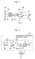
- Fig. 1 is a circuit diagram that shows this electrostatic capacitance detection circuit.
- a capacitive sensor 92 comprised of electrodes 90 and 91 is connected to an inverting input terminal of an operational amplifier 95 via a signal line 93.
- a capacitor 96 is connected between an output terminal of this operational amplifier 95 and the said inverting input terminal, and further an AC voltage Vac is applied to a non-inverting input terminal.
- the said signal line 93 is wrapped up by a shield line 94 and shielded electrically against disturbance noise.
- this shield line 94 is connected to the non-inverting input terminal of the operational amplifier 95.
- Output voltage Vd is obtained from an output terminal of the said operational amplifier 95 via a transformer 97.
- the inverting input terminal and the non-inverting input terminal of the operational amplifier 95 are in an imaginary short status, so that the signal line 93 connected to the inverting input terminal and the shied line 94 connected to the non-inverting input terminal have the almost same potential.
- the signal line 93 is guarded by the shield line 94, that is, stray capacitance between the signal line 93 and the shield line 94 is canceled, and the output voltage Vd, which is unlikely to be affected by the stray capacitance, can be obtained.
- This invention is devised in view of the above-mentioned situation, and aims at providing an impedance detection circuit, an electrostatic capacitance detection circuit and the like that are capable of accurately detecting very small capacitance change, and suitable to detect impedance, such as a capacitive sensor including a capacitor microphone used for lightweight and compact audio communication devices.
- the electrostatic capacitance detection circuit is an impedance detection circuit that outputs a detection signal corresponding to impedance of an impedance element to be detected, comprising: an impedance converter of which input impedance is high and output impedance is low; a first capacitive impedance element; a first operational amplifier; a DC voltage generator that applies DC voltage to the first operational amplifier; and a signal output terminal that is connected to an output of the first operational amplifier, wherein an input terminal of the impedance converter is connected to one end of the impedance element to be detected and one end of the first impedance element, the first impedance element and the impedance converter are included in a negative feedback loop of the first operational amplifier, and the impedance element to be detected and the impedance detection circuit are located adjacently.
- the electrostatic capacitance detection circuit is an impedance detection circuit that outputs a detection signal corresponding to impedance of an impedance element to be detected, comprising: an impedance converter of which input impedance is high and output impedance is low; a first capacitive impedance element; a first operational amplifier; a DC voltage generator that applies DC voltage to the first operational amplifier; and a signal output terminal that is connected to an output of the first operational amplifier, wherein an input terminal of the impedance converter is connected to one end of the impedance element to be detected and one end of the first impedance element, the first impedance element and the impedance converter are included in a negative feedback loop of the first operational amplifier, and the impedance element to be detected, the first impedance element and the impedance converter are located closely.
- an impedance detection method and an electrostatic capacitance detection method is an impedance detection method that outputs a detection signal corresponding to impedance of an impedance element to be detected, comprising steps for: connecting a first capacitive impedance element between an output terminal of an operational amplifier and an input terminal of an impedance converter; connecting the impedance element to be detected between the input terminal of the impedance converter and specific potential; applying DC voltage to one input terminal of the operational amplifier via a resistance, and other input terminal of the operational amplifier is connected to specific potential; outputting voltage that comes out at the output terminal of the operational amplifier as a detection signal; and connecting the impedance element to be detected, the impedance converter and the first impedance element closely.
- the electrostatic capacitance detection circuit is structured to comprise a DC voltage generator, a operational amplifier of which non-inverting input terminal is connected to specific potential, an impedance converter, a resistance (R2) connected between an inverting input terminal of the operational amplifier and an output terminal of the impedance converter, a capacitive impedance element connected between the output terminal of the operational amplifier and the input terminal of the impedance converter.
- An impedance to be detected is located adjacently to this impedance detection circuit, or set closely to the impedance detection circuit at a short distance that does not make the stray capacitance of the signal line exceed ten times as much as maximum capacitance of an element connected, and connected between the input terminal and the specific potential.
- the specific potential in the example here indicates either certain standard potential, specific DC potential, ground potential or a floating status, whichever suitable is selected according to a style of an embodiment.
- a resistance (R1) connected between the DC voltage generator and the inverting input terminal of the operational amplifier may further be added.
- a certain voltage is applied to the impedance to be detected, most of electric current that flows through the impedance to be detected is further sent to the impedance element, and then a signal corresponding to the impedance of the impedance to be detected is output from a signal output terminal.
- a resistance may be connected in parallel with the impedance element.
- one end of the impedance to be detected and the input terminal of the impedance converter may be connected each other by a signal line covered with a shielding material, and a guard voltage applying unit that applies specific voltage to the shielding material may be added.
- the specific potential means some discretional regular potential, preferably a ground, but it may be the same potential as that of the voltage of the signal line. Actions of the circuit are stabilized by the specific voltage applied to the shielding material.
- the guard voltage applying unit is, for example, a unit that generates a certain voltage using output voltage of the DC voltage generator or output voltage of the impedance converter as an input, or a unit that connects the shielding material to the ground.
- the impedance converter may be made up of a voltage follower, or a voltage amplifier of which voltage gain is less than or more than 1. Then, when an input side of the impedance converter is made up of a circuit comprising MOSFET, the input impedance may further be enhanced.
- the impedance to be detected is a capacitance type of sensor that detects a physical quantity according to a fluctuation in the capacitance, that the electrostatic capacitance detection circuit as the impedance detection circuit is formed on a printed circuit board or a silicon substrate, and that the capacitance type of sensor and the board are fixed.
- a capacitor microphone is adopted as the impedance to be detected, that the electrostatic capacitance detection circuit is embodied by an IC, that the capacitor microphone and the IC are integrated into one and put in a shield box as a microphone used for a mobile phone or the like.
- the capacitor microphone and the IC are fixed adjacently and connected with a conductive board, a wiring pattern, a wire bonding or the like.
- Fig. 2 is a circuit diagram of an impedance detection circuit according to a first embodiment of the present invention.
- a capacitor to be detected 17 i.e. a capacitance type sensor that detects various types of physical quantities using a fluctuation in the electrostatic capacitance Cs such as a capacitor microphone in this example.
- an electrostatic capacitance detection circuit 10 as the impedance detection circuit.
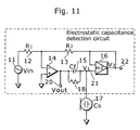
- This electrostatic capacitance detection circuit 10 comprises an DC voltage generator 11 that generates AC voltage, a resistance (R1) 12, a resistance (R2) 13, an operational amplifier 14, an impedance element 15 (a capacitor with capacitance Cf in this example) and an impedance converter 16, and outputs a detection signal (voltage V out) corresponding to a temporal change in electrostatic capacitance of the capacitor 17 from a signal output terminal 20.
- the "temporal change” here includes changes with respect to a frequency or a pulse, gradual changes, random changes with time, and so on, and it may not necessarily indicate periodicity.
- the resistance (R1) 12 is connected between the output terminal of the DC voltage generator 11 and an inverting input terminal of the operational amplifier 14.
- the operational amplifier 14 is a voltage amplifier of which input impedance and open loop gain are extremely high, a non-inverting input terminal here is connected to specific potential (the ground in this example), and the non-inverting input terminal and the inverting input terminal are in an imaginary short status.
- the capacitor 15, the impedance converter 16 and the resistance (R2) 13 are connected in series in this order.
- the impedance converter 16 is a voltage amplifier of which input impedance is extremely high, output impedance is extremely low, and voltage gain is A times.
- An input terminal 21 of this impedance converter 16 is connected to one end of the capacitor 17, and other end of the capacitor 17 is connected to the specific potential (the ground in this example).
- An output terminal of the operational amplifier 14 is connected to an output signal of this electrostatic capacitance detection circuit 10, i.e. the signal output terminal 20 for outputting a detection signal corresponding to a change in the capacitance value of the capacitor 17.
- a variable A indicated for A times or the like in this patent document shows any real number other than zero.
- Actions of the electrostatic capacitance detection circuit 10 structured above are as follows.
- V2 - (R2 / R1) ⁇ Vin
- the input voltage V1 is as follows from a relationship between the input voltage (voltage of the input terminal 21) V1 and the output voltage (voltage of the output terminal 22) V2.
- V1 (1 / A) ⁇ V2
- V1 - (R2 / R1) ⁇ (Vin / A)
- ⁇ Vout for the change in the output voltage Vout of the detection signal becomes a value in proportion to ⁇ Cs for the change in the capacitance Cs of the capacitor 17. Therefore, a signal corresponding to the sound input to the capacitor microphone can be obtained by extracting only ⁇ Vout, which is the DC component of the detection signal output from this electrostatic capacitance detection circuit 10. Then, it is possible to largely amplify the net signal corresponding to the sound (the voltage corresponding to ⁇ Cs), and a highly sensitive microphone can be realized.
- a proportionality constant k shown in the above expression 6 does not contain an item that depends on the frequency (the sound frequency), and is a fixed value. Therefore, this electrostatic capacitance detection circuit 10 does not depend on the sound frequency, and with a fixed gain, it outputs a faithful voltage signal corresponding to loudness of the sound.
- actions of the capacitor 17 have been examined from a viewpoint of voltage. When it is analyzed from an angle of electric current for better understanding, it is as follows.
- Cd is standard capacitance originally and basically held by the capacitor 17
- ⁇ C is a peak value of the change
- ⁇ c is a frequency that changes the capacitance being detected for the capacitor 17.
- this electrostatic capacitance detection circuit 10 is operated by a DC drive (the DC voltage generator 11), it is steadily functioned when compared with a case of an AC drive so that noise or the like can be restrained. Furthermore, parts for the DC transmitter, etc. become unnecessary, and thereby size of the circuit can be reduced.
- Fig. 3 is a specific circuit example of the impedance converter 16 in the electrostatic capacitance detection circuit 10 shown in Fig. 2.
- Fig. 3 A shows a voltage follower 16a using an operational amplifier 30. An inverting input terminal and an output terminal of the operational amplifier 30 are short-circuited.
- the impedance converter 16, of which input impedance is extremely high and voltage gain A becomes 1, can be obtained by making a non-inverting input terminal of this operational amplifier 30 be an input of the impedance converter 16, and making the output terminal of the operational amplifier 30 be an output of the impedance converter 16.
- Fig. 3 B shows a non-inverting amplifier circuit 16b using an operational amplifier 31.
- a resistance (R3) 32 is connected between an inverting input terminal of the operational amplifier 31 and specific potential, and a feedback resistance (resistance (R4) 33) is connected between the inverting input terminal and the output terminal of the operational amplifier 31.
- the impedance converter 16, of which input impedance is extremely high and voltage gain A becomes (R3 + R4) / R3, can be obtained by making a non-inverting input terminal of this operational amplifier 31 be an input of the impedance converter 16, and making the output terminal of the operational amplifier 31 be an output of the impedance converter 16.
- Fig. 3 C shows a circuit 16c where a buffer in CMOS structure is added to an input side of the operational amplifier as shown in Fig. 3 A or B.
- N type MOSFET34 and P type MOSFET35 are connected in series between negative and positive power supplies via a resistance, and an output of the buffer is connected to the input of the operational amplifier 30 (or 31).
- the impedance converter 16, of which input impedance is extremely high, can be obtained by making the input of this buffer be an input of the impedance converter 16, and making the output terminal of the operational amplifier be an output of the impedance converter 16.
- Fig. 3 D shows a circuit 16d that is like a buffer at the input side of Fig. 3 C.
- N type MOSFET 34 and P type MOSFET 35 are connected in series between the positive and negative power supplies, and the output is made from a connection point of both MOSFET.
- Fig. 3 E is a circuit where a non-inverting input of an operational amplifier 32 is made to be an input of the impedance converter, and an output and the inverting input of the operational amplifier 32 are connected each other via a resistance. As shown in Fig. 3 D and E, having such structure realizes the impedance converter 16 of which input impedance is extremely high.
- the electrostatic capacitance detection circuit shown in Fig. 2 for example, if the stray capacitance of the signal line exceeds 200pF when original electrostatic capacitance of Cs (an impedance to be detected: a microphone in the present embodiment) is 20pF, the detection sensitivity becomes much worse. Also, when the said Cs is checked with a few other electrostatic capacitance values, their results tend to be the same.
- Cs an impedance to be detected: a microphone in the present embodiment
- both of the capacitance Cf, which is the first impedance element, and the capacitor Cs are a capacitance element connected to the signal line in this circuit, so that the same result as above is expected for calculation of both of the elements.
- Fig. 4 is a circuit diagram of an electrostatic capacitance detection circuit 40 as the impedance detection circuit according to the second embodiment of the present invention.
- This electrostatic capacitance detection circuit 40 is equivalent to what a guarding function is added to the electrostatic capacitance detection circuit 10 according to the first embodiment. That is, as a cable to connect the capacitor 17 with the electrostatic capacitance detection circuit 40, a signal line 41 (a coaxial cable) covered with a shielding line 42 is used, and additionally a guard voltage applying circuit 43a for applying guard voltage, of which potential is the same as that of the signal line 41, is added to the shielding line 42 of the coaxial cable.
- the guard voltage applying circuit 43a By making the guard voltage applying circuit 43a be connected between the output terminal of the DC voltage generator 11 and the shielding line 42, receiving the output voltage Vin of the DC voltage generator 11 as an input, and amplifying the voltage (or dividing the voltage) with a certain pre-adjusted voltage gain, the guard voltage applying circuit 43a serves as a DC voltage amplifier that generates guard voltage, of which potential is the same as that of the voltage of the signal line 41, and that outputs and applies the guard voltage to the shielding line 42.
- the voltage gain of this guard voltage applying circuit 43a is specifically V1 / Vin, that is, as seen from the above expression 4, adjusted to (-R2 / R1) ⁇ (1 / A).
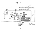
- a connection point of the guard voltage applying circuit 43a that applies guard voltage to the shielding line 42 is not limited to an area between the DC voltage generator 11 and the shielding line 42 shown in Fig. 4, and it may be located to an area between the output terminal of the impedance converter 16 and the shielding line 42, for example, like the electrostatic capacitance detection circuit 45 shown in Fig. 5.
- a guard voltage applying circuit 43b (or 43c) may be adjusted to generate guard voltage V1 and apply the voltage to the shielding line 42.
- the guard voltage applying circuit is only limited to DC applying, the cancellation effect of the stray capacitance cannot be expected. In such a case, it is effective to have ground connection in simple structure where any disturbance noise is not easily mixed in.
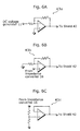
- Fig. 6 shows specific circuit examples of the guard voltage applying circuits 43a ⁇ c indicated in Fig. 4 and 5.
- the guard voltage applying circuit 43a shown in Fig. 6 A is an inverting amplification circuit having its variable resistance as a feedback resistance. The above voltage gain can be obtained by adjusting the resistance value of the feedback resistance, and the guard voltage, of which potential is the same as that of the signal line 41, can be generated.
- the guard voltage applying circuit 43b shown in Fig. 6 B is a non-inverting amplification circuit composed of two resistances and one operational amplifier.
- the guard voltage applying circuit 43c shown in Fig. 6 C is a voltage follower composed of two resistances and one operational amplifier.
- the guard voltage, of which potential is the same as that of the signal line 41 in Fig. 5, can also be generated by adjusting the values of the resistance in these Fig. 6 B and C.
- the impedance to be detected is a sensor that detects a physical quantity according to a fluctuation in the impedance, that the impedance detection circuit is formed on a printed circuit board or a silicon substrate, and that the sensor and the board or the substrate are fixed and integrated into one.
- a capacitor microphone is adopted as the impedance to be detected, that the electrostatic capacitance detection circuit is embodied by an IC, that the capacitor microphone and the IC are integrated into one and put in a shield box as a microphone used for a mobile phone or the like.
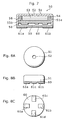
- Fig. 7 is a diagram showing a practical example to use the electrostatic capacitance detection circuit according to the first embodiment for an electric device.
- it shows a cross section diagram of a microphone 50 used for a mobile phone or the like which comprises a capacitor microphone and an electrostatic capacitance detection circuit that are integrated into one.
- This microphone 50 comprises a lid cover 51 having a sound hole 52, an oscillating film 53 that oscillates with sounds, a ring 54 that fixes the oscillating film 53, a spacer 55a, a fixed electrode 56 set up against the oscillating film 53 via the spacer 55a, an isolation board 55b that supports the fixed electrode 56, an IC chip 58 forming the electrostatic capacitance detection circuit according to the above embodiment, which is fixed on a backside of the isolation board 55b, an IC package 59 that molds the IC chip 58, external electrodes 61a and 61b that are connected by the IC chip 58, a wire bonding, a contact hole, and the like.
- the oscillating film 53 which is one side of the electrodes that forms the capacitor, is connected to specific potential (a ground in this example), and the fixed electrode 56, which is the other side of the electrodes, is connected to a circuit of the IC chip 58 via an electric conductor such as an aluminum board or a wire bonding.
- Capacitance and a change in the capacitance of the capacitor comprising the oscillating film 53 and the fixed electrode 56 are detected by the electrostatic capacitance detection circuit in the IC chip 58 located adjacently via the isolation board 55b, transformed into an electric signal, and output from the external electrodes 61a and 61b, or the like.
- the lid cover 51 which is made from a metal such as aluminum, serves as a role of a shield box that shields any disturbance noise mixed into the inner capacitors 53 and 56, and the IC chip 58 with a conductive film (not shown) formed on an upper surface of the isolation board 60.
- the fixed electrode 56 is connected to the circuit, and the oscillating film 53 is connected to specific potential.
- the oscillating film 53 may be connected to the circuit, and the fixed electrode 56 may be connected to the specific potential. But, the former case is preferable from past experiences.
- Fig. 8 is an external view diagram showing an outline of the microphone 50 shown in Fig. 7.
- Fig. 8 A is a plain diagram
- Fig. 8 B is a front view diagram
- Fig. 8 C is a bottom view diagram.
- Size of the lid cover 51 shown in Fig. 8 A and Fig. 8 B is, for example, approximately ⁇ 5 mm x 2 mm in height.
- Four external electrodes 61a ⁇ 61d shown in Fig. 8 C are, for example, two terminals for a power supply and two terminals for an output signal of the electrostatic capacitance detection circuit.
- the capacitor to be detected (the capacitor microphone in the example here) and the electrostatic capacitance detection circuit (the IC chip in the example here) are located adjacently to be in contact side by side under the aforementioned condition for being closely, and they are connected each other by an electric conductor of which length is extremely short. Then, these parts are covered with a shield material such as a metal lid cover. Therefore, in the practical example like this, any negative impacts such as disturbance noise, which is mixed into the signal line (the electric conductor) connecting the impedance to be detected and the electrostatic capacitance detection circuit, can be ignored.
- the capacitor to be detected and the electrostatic capacitance detection circuit are connected each other by a non-shielded (unshielded) conductive board, wiring pattern, wire bonding, lead line or the like through a shortest route. That is, in this practical example, since it may be applied to a compact microphone where a shielding material is not used for its signal line, the capacitor to be detected and the electrostatic capacitance detection circuit are connected each other by an extremely short electric conductor, and a special circuit for applying guard voltage to the shield or the like is not located, so that the size of the circuit doesn't get bigger and miniaturization of the circuit is not hindered.
- Fig. 9 and Fig. 10 show the circuit put on a board. They are basically the same as the one in Fig. 7 with an exception that the electrostatic capacitance detection circuit is put on a board 62.
- the size of the circuit gets a little bigger for a part of the shield of the signal line.
- this structure may be used since this is rather preferable for more accurate measurement.
- the impedance detection circuit and the electrostatic capacitance detection circuit according to the present invention have been described based on the two embodiments, the present invention is not limited to these embodiments.
- one layered shield cable is used as a cable to connect the capacitor 17 and the electrostatic capacitance detection circuit 40
- two layered shield cable can be used in stead.
- the guard voltage is applied to its inner shield covering the signal line, and its outer shield covering the inner shield is connected to the specific potential or the ground, so that a shielding effect against disturbance noise can be enhanced.
- a resistance 18 in parallel with the capacitor 15 in the electrostatic capacitance detection circuits 10 and 30 it is possible to connect a resistance 18 in parallel with the capacitor 15 in the electrostatic capacitance detection circuits 10 and 30 according to the above embodiments. In this way, a connecting point for the capacitor 15 and the capacitor 17 is connected to the output terminal of the operational amplifier 14 via the resistance 18, so that having a floating status through a DC form can be avoided and the potential can be fixed.
- a device connected as the impedance to be connected is not limited to a capacitor microphone and includes all of devices, which detect various physical quantities such as an acceleration sensor, a seismograph, a pressure sensor, a displacement sensor, a proximity sensor, a touch sensor, an ion sensor, a humidity sensor, a raindrop sensor, a snow sensor, a thunder sensor, a placement sensor, a bad contact sensor, a configuration sensor, an endpoint detection sensor, an oscillation sensor, an ultrasonic wave sensor, an angular velocity sensor, a liquid quantity sensor, a gas sensor, an infrared rays sensor, a radiation sensor, a water gauge, a freeze sensor, a moisture meter, a vibrometer, an electrification sensor, a publicly-known capacitive type sensor like a printed circuit board inspection device, or the like.
- the impedance detection circuit As has been clarified from the above explanation, by applying DC voltage to the operational amplifier and connecting the impedance to be detected to the signal line, the impedance detection circuit, the electrostatic capacitance detection device and their method according to the present invention detect impedance of the impedance to be detected. That is, the capacitor is connected between the output terminal of the operational amplifier, of which non-inverting input terminal is connected to the specific potential, and the input terminal of the impedance converter, and further the impedance to be detected is connected between the input terminal of the impedance converter and the specific potential.
- the operational amplifier is functioned steadily, and the noise mixed in the detection signal is restrained. Also, as the entire detection circuit is operated by the DC drive and does not require a DC signal transmitter or the like, it can be simplified and miniaturized.
- the capacitor since the capacitor is connected between the operational amplifier and the impedance converter, it does not cause a problem to degrade an S/N ratio due to thermal noise from the resistance when a resistance is connected between the operational amplifier and the impedance converter.
- a change component which corresponds to the change in the impedance of the impedance to be detected, is generated at the output terminal of the operational amplifier by extracting only the change component of the output terminal, it realizes an operational amplifier that is best suitable to a capacitive sensor of which capacitance is changed according to the change in the physical quantity of the capacitor microphone or the like.
- a microphone which detects sound with extremely high sensitivity, can be realized.
- the present invention realizes an electrostatic capacitance detection circuit or the like, which detects very small impedance and capacitance accurately, and is suitable for miniaturization, and especially sound performance of lightweight and compact audio communication devices such as a mobile phone is rapidly improved and its practical value is extremely high.
- the electrostatic capacitance detection circuit according to the present invention may be used as a detection circuit of a capacitance type sensor, especially as a microphone device that is equipped with compact and lightweight devices such as a mobile phone.
Landscapes
- Physics & Mathematics (AREA)
- General Physics & Mathematics (AREA)
- Health & Medical Sciences (AREA)
- General Health & Medical Sciences (AREA)
- Otolaryngology (AREA)
- Engineering & Computer Science (AREA)
- Acoustics & Sound (AREA)
- Signal Processing (AREA)
- Measurement Of Resistance Or Impedance (AREA)
- Circuit For Audible Band Transducer (AREA)
- Investigating Or Analyzing Materials By The Use Of Electric Means (AREA)
- Networks Using Active Elements (AREA)
Abstract
Description


Claims (15)
- An impedance detection circuit that outputs a detection signal corresponding to impedance of an impedance element to be detected, comprising:wherein an input terminal of the impedance converter is connected to one end of the impedance element to be detected and one end of the first impedance element,an impedance converter of which input impedance is high and output impedance is low;a first capacitive impedance element;a first operational amplifier;a DC voltage generator that applies DC voltage to the first operational amplifier; anda signal output terminal that is connected to an output of the first operational amplifier,
the first impedance element and the impedance converter are included in a negative feedback loop of the first operational amplifier, and
the impedance element to be detected and the impedance detection circuit are located adjacently. - An impedance detection circuit that outputs a detection signal corresponding to impedance of an impedance element to be detected, comprising:wherein an input terminal of the impedance converter is connected to one end of the impedance element to be detected and one end of the first impedance element,an impedance converter of which input impedance is high and output impedance is low;a first capacitive impedance element;a first operational amplifier;a DC voltage generator that applies DC voltage to the first operational amplifier; anda signal output terminal that is connected to an output of the first operational amplifier,
the first impedance element and the impedance converter are included in a negative feedback loop of the first operational amplifier, and
the impedance element to be detected, the first impedance element and the impedance converter are located closely. - The impedance detection circuit according to Claim 1 or 2,
wherein the impedance element to be detected is a capasitive impedance element. - The impedance detection circuit according to any of Claims 1 through 3, further comprising a resistance element connected in parallel with the first impedance element.
- The impedance detection circuit according to any of Claims 1 through 4, further comprising a second impedance element connected between the DC voltage generator and the first operational amplifier.
- The impedance detection circuit according to any of Claims 1 through 5,
wherein the one end of the impedance element to be detected and the input terminal of the impedance converter are connected each other by a signal line covered with a shielding material, and
the impedance detection circuit further includes a guard voltage applying unit that applies specific voltage to the shielding material. - The impedance detection circuit according to Claims 6,
wherein the guard voltage applying unit receives output voltage of the DC voltage generator as an input. - The impedance detection circuit according to Claims 6,
wherein the guard voltage applying unit receives output voltage of the impedance converter as an input. - The impedance detection circuit according to any of Claims 1 through 8,
wherein the impedance converter is a voltage follower. - The impedance detection circuit according to any of Claims 1 through 8,
wherein the impedance converter is a voltage amplification circuit that includes a second operational amplifier and has a voltage gain bigger than one. - The impedance detection circuit according to any of Claims 1 through 8,
wherein the impedance converter includes an input circuit composed of MOSFET and a second operational amplifier. - The electrostatic capacitance detection circuit according to any of Claims 1 through 11,
wherein the impedance element to be detected is a capacitive sensor of which capacitance is changed temporally, and the first impedance element is a capacitor. - The electrostatic capacitance detection circuit according to Claim 12,
wherein the impedance element to be detected is a capacitor microphone. - An impedance detection method that outputs a detection signal corresponding to impedance of an impedance element to be detected, comprising steps for:connecting a first capacitive impedance element between an output terminal of an operational amplifier and an input terminal of an impedance converter;connecting the impedance element to be detected between the input terminal of the impedance converter and specific potential;applying DC voltage to one input terminal of the operational amplifier via a resistance, and other input terminal of the operational amplifier is connected to specific potential;outputting voltage that comes out at the output terminal of the operational amplifier as a detection signal; andconnecting the impedance element to be detected, the impedance converter and the first impedance element closely.
- The impedance detection method according to Claims 14,
wherein one end of the impedance element to be detected and the input terminal of the impedance converter are connected each other by a signal line covered with a shielding material, and
specific voltage is applied to the shielding material.
Applications Claiming Priority (3)
| Application Number | Priority Date | Filing Date | Title |
|---|---|---|---|
| JP2001270877 | 2001-09-06 | ||
| JP2001270877 | 2001-09-06 | ||
| PCT/JP2002/009137 WO2003023420A1 (en) | 2001-09-06 | 2002-09-06 | Impedance measuring circuit, its method, and capacitance measuring circuit |
Publications (3)
| Publication Number | Publication Date |
|---|---|
| EP1426772A1 true EP1426772A1 (en) | 2004-06-09 |
| EP1426772A4 EP1426772A4 (en) | 2005-08-03 |
| EP1426772B1 EP1426772B1 (en) | 2008-03-12 |
Family
ID=19096476
Family Applications (1)
| Application Number | Title | Priority Date | Filing Date |
|---|---|---|---|
| EP02767921A Expired - Lifetime EP1426772B1 (en) | 2001-09-06 | 2002-09-06 | Impedance measuring circuit, its method, and capacitance measuring circuit |
Country Status (9)
| Country | Link |
|---|---|
| US (1) | US7005865B2 (en) |
| EP (1) | EP1426772B1 (en) |
| KR (1) | KR100654471B1 (en) |
| CN (1) | CN100454028C (en) |
| AT (1) | ATE389185T1 (en) |
| DE (1) | DE60225570T2 (en) |
| NO (1) | NO20032013L (en) |
| TW (1) | TWI221196B (en) |
| WO (1) | WO2003023420A1 (en) |
Cited By (1)
| Publication number | Priority date | Publication date | Assignee | Title |
|---|---|---|---|---|
| NL2007186C2 (en) * | 2011-07-28 | 2013-01-29 | Fluid Well Instr B V | FOR HIGH FREQUENT FAULTS UNSENSITIVE CAPACITIVE MEASUREMENT SWITCH. |
Families Citing this family (17)
| Publication number | Priority date | Publication date | Assignee | Title |
|---|---|---|---|---|
| US8247883B2 (en) * | 2008-12-04 | 2012-08-21 | Palo Alto Research Center Incorporated | Printing shielded connections and circuits |
| JP5544717B2 (en) * | 2009-01-15 | 2014-07-09 | 富士通株式会社 | Semiconductor device and test method |
| US8362784B2 (en) * | 2009-06-22 | 2013-01-29 | Mitsubishi Electric Corporation | Capacitor capacitance diagnosis device and electric power apparatus equipped with capacitor capacitance diagnosis device |
| JP2013061177A (en) * | 2011-09-12 | 2013-04-04 | Nidec-Read Corp | Impedance measuring device |
| DE102011083052B4 (en) * | 2011-09-20 | 2016-03-10 | Hauni Maschinenbau Ag | Capacitive HF strand measuring device and stranding machine |
| US9645193B2 (en) | 2012-10-23 | 2017-05-09 | Keithley Instruments, Llc | Impedance source ranging apparatus and method |
| WO2014107843A1 (en) * | 2013-01-08 | 2014-07-17 | Zhihao Yang | Condenser microphone and its impedance converter |
| CN103344172B (en) * | 2013-07-09 | 2015-08-12 | 中国工程物理研究院总体工程研究所 | A kind of capacitance gage acquisition processing device and method reducing electromagnetic pulse interference |
| CN105277786A (en) * | 2014-07-25 | 2016-01-27 | 南京瀚宇彩欣科技有限责任公司 | Method for detecting maximum impedance of sensor and detection device |
| CN104640053A (en) | 2015-01-19 | 2015-05-20 | 矽力杰半导体技术(杭州)有限公司 | Direct-current impedance detecting method of loudspeaker, circuit and D type audio frequency amplifier |
| CN106341763B (en) | 2016-11-17 | 2019-07-30 | 矽力杰半导体技术(杭州)有限公司 | Speaker driving device and speaker driving method |
| CN106454679B (en) * | 2016-11-17 | 2019-05-21 | 矽力杰半导体技术(杭州)有限公司 | State estimation method of loudspeaker diaphragm and loudspeaker drive circuit using the same |
| CN107422192B (en) * | 2017-08-02 | 2020-05-08 | 广州市锐丰音响科技股份有限公司 | Audio equipment input impedance measuring method and device and measurement and verification method and device |
| CN107274644A (en) * | 2017-08-11 | 2017-10-20 | 四川赛科安全技术有限公司 | A kind of method for detecting fire-fighting bus capacitive size |
| WO2019187515A1 (en) * | 2018-03-30 | 2019-10-03 | パナソニックIpマネジメント株式会社 | Capacitance detection device |
| CN108693408B (en) * | 2018-08-22 | 2020-07-07 | 广东电网有限责任公司 | Supercapacitor internal resistance detection method and device and computer readable storage medium |
| CN114812618B (en) * | 2021-12-24 | 2023-03-07 | 中国科学院长春光学精密机械与物理研究所 | Frequency Noise Suppression System |
Family Cites Families (13)
| Publication number | Priority date | Publication date | Assignee | Title |
|---|---|---|---|---|
| DE3221800A1 (en) * | 1982-06-05 | 1983-12-08 | Martin Dipl Ing Kueper | Measurement method for determining loudspeaker data |
| US4918376A (en) * | 1989-03-07 | 1990-04-17 | Ade Corporation | A.C. capacitive gauging system |
| DK170196B1 (en) | 1993-04-07 | 1995-06-06 | Brueel & Kjaer As | Method and coupling to reduce the harmonic distortion of a capacitive transducer |
| JPH09280806A (en) | 1996-04-09 | 1997-10-31 | Nissan Motor Co Ltd | Capacitance type displacement meter |
| DK0970386T3 (en) * | 1998-01-23 | 2006-11-13 | Tokyo Electron Ltd | Impedance-to-voltage converter |
| CN1211666C (en) * | 1998-02-05 | 2005-07-20 | 东京毅力科创株式会社 | Impedance-to-voltage converter and converting method |
| TW418323B (en) * | 1998-02-19 | 2001-01-11 | Sumitomo Metal Ind | Capacitance detection system and method |
| JP4124867B2 (en) * | 1998-07-14 | 2008-07-23 | 松下電器産業株式会社 | Conversion device |
| JP3501401B2 (en) * | 2000-03-07 | 2004-03-02 | 住友金属工業株式会社 | Impedance detection circuit, impedance detection device, and impedance detection method |
| JP3454426B2 (en) * | 2000-07-10 | 2003-10-06 | 住友金属工業株式会社 | Impedance detection circuit and impedance detection method |
| JP3501398B2 (en) | 2000-07-10 | 2004-03-02 | 住友金属工業株式会社 | Impedance detection circuit and impedance detection method |
| JP2002157671A (en) * | 2000-11-16 | 2002-05-31 | Sumitomo Metal Ind Ltd | Sensing system |
| ITTO20010699A1 (en) * | 2001-07-17 | 2003-01-17 | St Microelectronics Srl | METHOD AND CIRCUIT FOR DETECTION OF MOVEMENTS THROUGH MICRO-ELECTRO-MECHANICAL SENSORS WITH COMPENSATION OF PARASITE CAPACITY AND MOVEMENT |
-
2002
- 2002-09-05 TW TW091120338A patent/TWI221196B/en not_active IP Right Cessation
- 2002-09-06 CN CNB028173929A patent/CN100454028C/en not_active Expired - Fee Related
- 2002-09-06 EP EP02767921A patent/EP1426772B1/en not_active Expired - Lifetime
- 2002-09-06 AT AT02767921T patent/ATE389185T1/en not_active IP Right Cessation
- 2002-09-06 WO PCT/JP2002/009137 patent/WO2003023420A1/en not_active Ceased
- 2002-09-06 DE DE60225570T patent/DE60225570T2/en not_active Expired - Lifetime
- 2002-09-06 US US10/488,679 patent/US7005865B2/en not_active Expired - Fee Related
- 2002-09-06 KR KR1020047003319A patent/KR100654471B1/en not_active Expired - Fee Related
-
2003
- 2003-05-05 NO NO20032013A patent/NO20032013L/en not_active Application Discontinuation
Cited By (2)
| Publication number | Priority date | Publication date | Assignee | Title |
|---|---|---|---|---|
| NL2007186C2 (en) * | 2011-07-28 | 2013-01-29 | Fluid Well Instr B V | FOR HIGH FREQUENT FAULTS UNSENSITIVE CAPACITIVE MEASUREMENT SWITCH. |
| EP2551643A1 (en) * | 2011-07-28 | 2013-01-30 | Fluid Well Instruments B.V. | Capacitive measuring circuit insensitive to high-frequency interference |
Also Published As
| Publication number | Publication date |
|---|---|
| CN1842712A (en) | 2006-10-04 |
| CN100454028C (en) | 2009-01-21 |
| EP1426772B1 (en) | 2008-03-12 |
| KR100654471B1 (en) | 2006-12-05 |
| DE60225570T2 (en) | 2009-04-23 |
| TWI221196B (en) | 2004-09-21 |
| US20050035771A1 (en) | 2005-02-17 |
| NO20032013D0 (en) | 2003-05-05 |
| WO2003023420A1 (en) | 2003-03-20 |
| KR20040040454A (en) | 2004-05-12 |
| DE60225570D1 (en) | 2008-04-24 |
| EP1426772A4 (en) | 2005-08-03 |
| ATE389185T1 (en) | 2008-03-15 |
| NO20032013L (en) | 2003-06-19 |
| US7005865B2 (en) | 2006-02-28 |
Similar Documents
| Publication | Publication Date | Title |
|---|---|---|
| EP1426772B1 (en) | Impedance measuring circuit, its method, and capacitance measuring circuit | |
| US6335642B1 (en) | Impedance-to-voltage converter | |
| US7019540B2 (en) | Electrostatic capacitance detection circuit and microphone device | |
| US7023223B2 (en) | Impedance measuring circuit and capacitance measuring circuit | |
| EP1424563B1 (en) | Capacitance measuring circuit, capacitance measuring instrument, and microphone device | |
| JP4488400B2 (en) | Impedance detection circuit | |
| JP4072400B2 (en) | Capacitance detection circuit, capacitance detection device, and microphone device | |
| KR100341966B1 (en) | Impedance-to-voltage converter and converting method | |
| JP2004184307A (en) | Capacitance detection circuit and capacitance detection method | |
| JP2003075481A (en) | Impedance detection circuit and capacitance detection circuit | |
| JP3454426B2 (en) | Impedance detection circuit and impedance detection method | |
| JP2003075486A (en) | Impedance detection circuit and capacitance detection circuit and method thereof | |
| JP4071582B2 (en) | Impedance detection circuit and method thereof | |
| JP4071581B2 (en) | Capacitance detection circuit, capacitance detection device, and microphone device | |
| JP4282321B2 (en) | Impedance detection device and impedance detection method | |
| JP4072401B2 (en) | Impedance detection circuit and capacitance detection circuit | |
| JP2003075484A (en) | Capacitance detection circuit and capacitance detection method |
Legal Events
| Date | Code | Title | Description |
|---|---|---|---|
| PUAI | Public reference made under article 153(3) epc to a published international application that has entered the european phase |
Free format text: ORIGINAL CODE: 0009012 |
|
| 17P | Request for examination filed |
Effective date: 20040226 |
|
| AK | Designated contracting states |
Kind code of ref document: A1 Designated state(s): AT BE BG CH CY CZ DE DK EE ES FI FR GB GR IE IT LI LU MC NL PT SE SK TR |
|
| AX | Request for extension of the european patent |
Extension state: AL LT LV MK RO SI |
|
| RAP1 | Party data changed (applicant data changed or rights of an application transferred) |
Owner name: TOKYO ELECTRON LIMITED |
|
| A4 | Supplementary search report drawn up and despatched |
Effective date: 20050622 |
|
| 17Q | First examination report despatched |
Effective date: 20060811 |
|
| GRAP | Despatch of communication of intention to grant a patent |
Free format text: ORIGINAL CODE: EPIDOSNIGR1 |
|
| GRAS | Grant fee paid |
Free format text: ORIGINAL CODE: EPIDOSNIGR3 |
|
| GRAA | (expected) grant |
Free format text: ORIGINAL CODE: 0009210 |
|
| AK | Designated contracting states |
Kind code of ref document: B1 Designated state(s): AT BE BG CH CY CZ DE DK EE ES FI FR GB GR IE IT LI LU MC NL PT SE SK TR |
|
| REG | Reference to a national code |
Ref country code: GB Ref legal event code: FG4D |
|
| REG | Reference to a national code |
Ref country code: CH Ref legal event code: EP |
|
| REG | Reference to a national code |
Ref country code: IE Ref legal event code: FG4D |
|
| REF | Corresponds to: |
Ref document number: 60225570 Country of ref document: DE Date of ref document: 20080424 Kind code of ref document: P |
|
| PG25 | Lapsed in a contracting state [announced via postgrant information from national office to epo] |
Ref country code: FI Free format text: LAPSE BECAUSE OF FAILURE TO SUBMIT A TRANSLATION OF THE DESCRIPTION OR TO PAY THE FEE WITHIN THE PRESCRIBED TIME-LIMIT Effective date: 20080312 |
|
| PG25 | Lapsed in a contracting state [announced via postgrant information from national office to epo] |
Ref country code: AT Free format text: LAPSE BECAUSE OF FAILURE TO SUBMIT A TRANSLATION OF THE DESCRIPTION OR TO PAY THE FEE WITHIN THE PRESCRIBED TIME-LIMIT Effective date: 20080312 |
|
| NLV1 | Nl: lapsed or annulled due to failure to fulfill the requirements of art. 29p and 29m of the patents act | ||
| PG25 | Lapsed in a contracting state [announced via postgrant information from national office to epo] |
Ref country code: BE Free format text: LAPSE BECAUSE OF FAILURE TO SUBMIT A TRANSLATION OF THE DESCRIPTION OR TO PAY THE FEE WITHIN THE PRESCRIBED TIME-LIMIT Effective date: 20080312 |
|
| PG25 | Lapsed in a contracting state [announced via postgrant information from national office to epo] |
Ref country code: SK Free format text: LAPSE BECAUSE OF FAILURE TO SUBMIT A TRANSLATION OF THE DESCRIPTION OR TO PAY THE FEE WITHIN THE PRESCRIBED TIME-LIMIT Effective date: 20080312 Ref country code: SE Free format text: LAPSE BECAUSE OF FAILURE TO SUBMIT A TRANSLATION OF THE DESCRIPTION OR TO PAY THE FEE WITHIN THE PRESCRIBED TIME-LIMIT Effective date: 20080612 Ref country code: PT Free format text: LAPSE BECAUSE OF FAILURE TO SUBMIT A TRANSLATION OF THE DESCRIPTION OR TO PAY THE FEE WITHIN THE PRESCRIBED TIME-LIMIT Effective date: 20080818 Ref country code: ES Free format text: LAPSE BECAUSE OF FAILURE TO SUBMIT A TRANSLATION OF THE DESCRIPTION OR TO PAY THE FEE WITHIN THE PRESCRIBED TIME-LIMIT Effective date: 20080623 Ref country code: CZ Free format text: LAPSE BECAUSE OF FAILURE TO SUBMIT A TRANSLATION OF THE DESCRIPTION OR TO PAY THE FEE WITHIN THE PRESCRIBED TIME-LIMIT Effective date: 20080312 |
|
| PG25 | Lapsed in a contracting state [announced via postgrant information from national office to epo] |
Ref country code: NL Free format text: LAPSE BECAUSE OF FAILURE TO SUBMIT A TRANSLATION OF THE DESCRIPTION OR TO PAY THE FEE WITHIN THE PRESCRIBED TIME-LIMIT Effective date: 20080312 |
|
| ET | Fr: translation filed | ||
| PLBE | No opposition filed within time limit |
Free format text: ORIGINAL CODE: 0009261 |
|
| STAA | Information on the status of an ep patent application or granted ep patent |
Free format text: STATUS: NO OPPOSITION FILED WITHIN TIME LIMIT |
|
| PG25 | Lapsed in a contracting state [announced via postgrant information from national office to epo] |
Ref country code: DK Free format text: LAPSE BECAUSE OF FAILURE TO SUBMIT A TRANSLATION OF THE DESCRIPTION OR TO PAY THE FEE WITHIN THE PRESCRIBED TIME-LIMIT Effective date: 20080312 |
|
| 26N | No opposition filed |
Effective date: 20081215 |
|
| PG25 | Lapsed in a contracting state [announced via postgrant information from national office to epo] |
Ref country code: MC Free format text: LAPSE BECAUSE OF NON-PAYMENT OF DUE FEES Effective date: 20080930 Ref country code: EE Free format text: LAPSE BECAUSE OF FAILURE TO SUBMIT A TRANSLATION OF THE DESCRIPTION OR TO PAY THE FEE WITHIN THE PRESCRIBED TIME-LIMIT Effective date: 20080312 Ref country code: BG Free format text: LAPSE BECAUSE OF FAILURE TO SUBMIT A TRANSLATION OF THE DESCRIPTION OR TO PAY THE FEE WITHIN THE PRESCRIBED TIME-LIMIT Effective date: 20080612 |
|
| REG | Reference to a national code |
Ref country code: CH Ref legal event code: PL |
|
| PG25 | Lapsed in a contracting state [announced via postgrant information from national office to epo] |
Ref country code: IE Free format text: LAPSE BECAUSE OF NON-PAYMENT OF DUE FEES Effective date: 20080908 |
|
| PG25 | Lapsed in a contracting state [announced via postgrant information from national office to epo] |
Ref country code: IT Free format text: LAPSE BECAUSE OF FAILURE TO SUBMIT A TRANSLATION OF THE DESCRIPTION OR TO PAY THE FEE WITHIN THE PRESCRIBED TIME-LIMIT Effective date: 20080312 |
|
| PG25 | Lapsed in a contracting state [announced via postgrant information from national office to epo] |
Ref country code: CY Free format text: LAPSE BECAUSE OF FAILURE TO SUBMIT A TRANSLATION OF THE DESCRIPTION OR TO PAY THE FEE WITHIN THE PRESCRIBED TIME-LIMIT Effective date: 20080312 |
|
| PG25 | Lapsed in a contracting state [announced via postgrant information from national office to epo] |
Ref country code: CH Free format text: LAPSE BECAUSE OF NON-PAYMENT OF DUE FEES Effective date: 20080930 Ref country code: LI Free format text: LAPSE BECAUSE OF NON-PAYMENT OF DUE FEES Effective date: 20080930 |
|
| PG25 | Lapsed in a contracting state [announced via postgrant information from national office to epo] |
Ref country code: LU Free format text: LAPSE BECAUSE OF NON-PAYMENT OF DUE FEES Effective date: 20080906 |
|
| PG25 | Lapsed in a contracting state [announced via postgrant information from national office to epo] |
Ref country code: TR Free format text: LAPSE BECAUSE OF FAILURE TO SUBMIT A TRANSLATION OF THE DESCRIPTION OR TO PAY THE FEE WITHIN THE PRESCRIBED TIME-LIMIT Effective date: 20080312 |
|
| PG25 | Lapsed in a contracting state [announced via postgrant information from national office to epo] |
Ref country code: GR Free format text: LAPSE BECAUSE OF FAILURE TO SUBMIT A TRANSLATION OF THE DESCRIPTION OR TO PAY THE FEE WITHIN THE PRESCRIBED TIME-LIMIT Effective date: 20080613 |
|
| PGFP | Annual fee paid to national office [announced via postgrant information from national office to epo] |
Ref country code: GB Payment date: 20120905 Year of fee payment: 11 |
|
| PGFP | Annual fee paid to national office [announced via postgrant information from national office to epo] |
Ref country code: DE Payment date: 20120829 Year of fee payment: 11 Ref country code: FR Payment date: 20120926 Year of fee payment: 11 |
|
| GBPC | Gb: european patent ceased through non-payment of renewal fee |
Effective date: 20130906 |
|
| REG | Reference to a national code |
Ref country code: FR Ref legal event code: ST Effective date: 20140530 |
|
| REG | Reference to a national code |
Ref country code: DE Ref legal event code: R119 Ref document number: 60225570 Country of ref document: DE Effective date: 20140401 |
|
| PG25 | Lapsed in a contracting state [announced via postgrant information from national office to epo] |
Ref country code: GB Free format text: LAPSE BECAUSE OF NON-PAYMENT OF DUE FEES Effective date: 20130906 |
|
| PG25 | Lapsed in a contracting state [announced via postgrant information from national office to epo] |
Ref country code: FR Free format text: LAPSE BECAUSE OF NON-PAYMENT OF DUE FEES Effective date: 20130930 Ref country code: DE Free format text: LAPSE BECAUSE OF NON-PAYMENT OF DUE FEES Effective date: 20140401 |