EP1424641A1 - Verfahren und Einrichtung zum ermitteln der minimalen oder maximalen schaltaktivität einer digitalschaltung - Google Patents
Verfahren und Einrichtung zum ermitteln der minimalen oder maximalen schaltaktivität einer digitalschaltung Download PDFInfo
- Publication number
- EP1424641A1 EP1424641A1 EP02026498A EP02026498A EP1424641A1 EP 1424641 A1 EP1424641 A1 EP 1424641A1 EP 02026498 A EP02026498 A EP 02026498A EP 02026498 A EP02026498 A EP 02026498A EP 1424641 A1 EP1424641 A1 EP 1424641A1
- Authority
- EP
- European Patent Office
- Prior art keywords
- digital circuit
- switching activity
- minimum
- estimated value
- test
- Prior art date
- Legal status (The legal status is an assumption and is not a legal conclusion. Google has not performed a legal analysis and makes no representation as to the accuracy of the status listed.)
- Granted
Links
Images
Classifications
-
- G—PHYSICS
- G06—COMPUTING OR CALCULATING; COUNTING
- G06F—ELECTRIC DIGITAL DATA PROCESSING
- G06F30/00—Computer-aided design [CAD]
- G06F30/30—Circuit design
- G06F30/32—Circuit design at the digital level
- G06F30/33—Design verification, e.g. functional simulation or model checking
- G06F30/3323—Design verification, e.g. functional simulation or model checking using formal methods, e.g. equivalence checking or property checking
-
- G—PHYSICS
- G06—COMPUTING OR CALCULATING; COUNTING
- G06F—ELECTRIC DIGITAL DATA PROCESSING
- G06F30/00—Computer-aided design [CAD]
- G06F30/30—Circuit design
- G06F30/32—Circuit design at the digital level
- G06F30/33—Design verification, e.g. functional simulation or model checking
Definitions
- the following invention relates to a method and an apparatus to determine a minimum or a maximum Switching activity of a digital circuit based on a functional one Model of the digital circuit, as well as a digital storage medium with control signals to carry out the process by means of a data processing device.
- a corresponding method is known from EP 863 470 A1, in which a method of generating the function of Power consumption of a functional model of a digital Circuit is described in which method a Circuit description is generated in which the power consumption can be determined.
- This circuit description will subjected to a simulation using input patterns to determine the function of the power consumption.
- the determined values for the power consumption disadvantageously depend decisive from the test patterns used or Input patterns.
- the quality of the estimate of the power consumption is therefore determined by the skill in the selection the test pattern determines, so that if chosen unfavorably Test patterns the power consumption is misjudged.
- the present invention is therefore based on the object a method or one set up to carry out the method Device as well as in connection with a programmable Data processing device for implementation of the method set up digital storage medium To create tax statements in which starting from a Description of a digital circuit's minimum or maximum Switching activity can be reliably determined.
- This verification happens according to the invention by attempting counter evidence, which is looking for an operating case in which the Switching activity of the digital circuit is even larger or smaller than the original estimate for the maximum or minimal switching activity of the digital circuit. The Performing this counter-evidence consists in trying an operational case locate who made the initial assumption disproves the estimate for the maximum or minimum Switching activity would actually be an extreme value.
- a demonstration mode of operation or a refusal mode of operation can be found that contradicts the original assumption the originally assumed estimated value in next step of the iteration increases or decreases to the actual value for the maximum or minimum switching activity to come closer to the digital circuit. If the maximum Switching activity is sought, is verified during the verification looking for a refutation operation in which the switching activity is greater than the estimated value in the respective step, and the estimate is increased to the next step if no refusal operation case can be found or nevertheless even higher switching activity of the digital circuit than that originally estimated estimate must be possible, and the estimate is lowered if there is no rebuttal operation can be found.
- the minimum switching activity of the digital circuit is searched, the verification for a refusal operation case wanted, in which the switching activity of Digital circuit lower than the estimated value in each Step is. If such a refute operation case is found, the estimate becomes the next step of the iteration further reduced, and will not be a refute operation found, the estimate is increased to the next step.
- the switching activity of the digital circuit can advantageously than the number of elements within the digital circuit be defined which is a logical state can save and within a time base to be selected change their state.
- the one Logical state can be saved, in particular flip-flops such as flip-flops.
- a clock of the digital circuit can be used, whereby preferably a change of logic state with every cycle each flip-flop or storage element may be possible should.
- the switching activity can thus be expressed as an integer which is related to a time base, where in usually the time base is a clock step so the Switching activity is a simple integer.
- the estimation value is advantageously obtained from an iteration step incremented or decremented to the next, which vary from iteration step to iteration step steadily decreased. In this way it approaches in the course of Iteration of the estimate for the maximum or minimum Switching activity more and more the respective actual value on.
- the step size of each iteration step can be changed to the next in various ways.
- a Possibility is the step size to the next iteration step cut in half or by a specific one Factor to share.
- an estimated value cannot be used, but instead part of a reference variable, which advantageously the theoretically maximum possible switching activity of the digital circuit equivalent.
- This theoretical maximum value the is to be used as the reference variable, in particular Number of flip-flops within the digital circuit. To the In this case, flip-flops are all circuit elements counted, which can save a logical state.
- the number of flip-flops is the theoretical maximum is preferably used for the switching activity only if a clock step of the digital circuit is used as the time base is used.
- the switching activity can also be a multiple of the number the flip-flops of the digital circuit are used, if as a time base also a multiple of cycle steps of the Digital circuit is used.
- Verification or finding a refutation operation case can be done in different ways.
- the verification is carried out by using of the model of the digital circuit one or more logical Functions are created that match the logical state on some or all occurring within the digital circuit Describe switching elements depending on an operating case.
- the sum of the circumstances becomes the operating case understood that reproducible to a certain state of the digital circuit.
- An operating case includes in particular a certain pattern of input variables and the initial state of time of the digital circuit, if this determines the behavior of the digital circuit.
- a goal at the verification is to refute the operation as possible easy to find.
- the at least one logical function that describes the behavior of the digital circuit
- the at least one logical function that describes the behavior of the digital circuit
- the method according to the invention can be based on a synthesizable circuit description or a formal Property suite to be performed.
- a property suite is a set of properties in a formal property language are formulated, such as Sugar or System Verilog Assertions.
- a property suite or a set of properties can be used in the Implementation of the method according to the invention in the verification the selection of formal properties within the Property suite are restricted. So it is possible to consider only some of the formal properties when testing, for example, to examine the relevant and in particular operating cases that occur in practice to restrict. This is particularly useful if if the use of the digital circuit provided in the Environment causes certain operating cases or groups from operating cases are excluded from the outset.
- the estimated value is without a previous one Verification set, with the first set Estimated value depending on the theoretical maximum Value is set for the switching activity.
- the maximum value is, in particular, as previously stated, the number of the flip-flops in the digital circuit.
- the first An estimate can be, for example, a fixed percentage the theoretical maximum switching activity.
- the iteration is terminated depending on an abort criterion and the estimate used at that time used as a value for the maximum or minimum switching activity.
- Various termination criteria are used for the iteration Conditions in question.
- the iteration be canceled as soon as the increment in the gradual Reduce a certain minimum value reached.
- This The minimum value represents the upper limit for the error in the Determine the minimum or maximum switching activity.
- the minimum value is chosen so that it is smaller as a required accuracy in determining the minimum and maximum switching activity.
- the iteration can be carried out after a specified number canceled by iteration steps.
- the last refute operation case determined to be present determined to win an operating case that to an at least essentially maximum or minimum Switching activity within the digital circuit leads.
- This Disproving operational case which can be interpreted as a test pattern can, can be used for further different tests become.
- the refutation operating case can be used for this to use a suitable model of digital circuit the minimum or maximum power consumption determine. Another method or computer program can do this be used when it is used for verification has been. Another model may also be used the digital circuit may be required as it is in the verification was used.
- refusal operation case can also be used for this be changing the design of the digital circuit, in particular the maximum switching activity of the digital circuit reduce.
- a refutation operation used to cover a coverage to determine which is the number of elements within represents the digital circuit used in the implementation of the The test was relevant or had an impact on the test to have.
- This coverage is always on at least related to a formal property of the digital circuit, compliance with the basis of the test or verification was.
- coverage can be both in relation to the search for the minimum switching activity as well as after the maximum switching activity and continue for various formal properties of the digital circuit or combinations of formal properties can be calculated.
- the coverage can be used for diagnostic purposes
- Digital circuit can be used.
- the cover or coverage not only the proportion of those that are decisive in the examination Display elements, but possibly also which of the elements of the digital circuit is decisive in the test were. In this way, for example, dead people Paths are determined within the digital circuit that no contribution to the fulfillment of the required formal properties deliver.
- the method according to the invention can in particular in a data processing device like a programmable calculator be carried out, the invention also in one Data medium implemented with suitable control instructions can be, the control instructions set up in this way are that a suitably set up programmable Data processing device after reading the control instructions executes the method according to the invention.
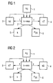
- Figure 1 is a schematic block diagram of the process steps when determining the maximum switching activity
- Figure 2 is a schematic block diagram of the process steps when determining the minimum switching activity of a Digital circuit.
- the minimum and the according to the inventive method determines maximum switching activity of a digital circuit, where the digital circuit in the form of a functional model with a number of properties defined, that the digital circuit fulfills.
- the switching activity uses the letter k, where the estimate of the switching activity and that at the end value of the switching activity not obtained in the method are called differently.
- the designation P (k) is used in the following to refute the at least one operational case to label the at least essentially leads to a certain switching activity k.
- the method begins with block 1, in which a starting value k 0 is specified as an estimated value of the switching activity.
- Block 1 is followed by block 2, which contains a verification as to whether the current estimated value k can actually be the maximum value for the switching activity or whether a refutation operating case can be found which refutes the assumption that the current estimated value k actually is the can be maximum value. If a refutation operating case is found and the assumption was false, the method branches to block 4, in which the estimated value k is increased by one step. If the assumption was true and no refutation operating case could be found, the process branches to block 3 by reducing the estimated value k by one step. Both the step size used in block 3 and in block 4 decrease with each process step.
- a check is also implemented within the query in block 2 as to whether the number of iteration steps already carried out has reached a maximum number.
- the verification block 2 ends the iteration and branches to the two blocks 5 and 6, in which in block 5 the current estimated value k is defined as the value for maximum switching activity of the digital circuit and in the other in block 6, the last refutation mode of operation P (k) determined as existing is determined and output.
- This last refutation mode of operation P (k) is used in further process steps, not shown, either for diagnostic purposes or for calculating the actual power consumption with maximum switching activity.
- the maximum power consumption of a digital circuit does not necessarily have to occur with the maximum switching activity, but this assumption is generally true.
- FIG. 2 shows the implementation of the method for the determination the minimum switching activity.
- the in Figure 2 in Blocks appearing in the block diagram correspond to those from FIG 1 and have been given the same reference numerals.
- the method shown in Figure 2 for the verification block 2 does not determine whether the estimated value k is the maximum could be, but whether it could and will be the minimum trying to find a refute operation case where the switching activity is even lower. If determined becomes that the assumption is false and the existence a suitable refutation mode of operation with less Switching activity could be proven to block 4 branches in which the estimated value k by one step reduced and the verification in block 2 is repeated.
- the system branches to block 3, there the estimated value k is increased by one step and the verification in block 2 is repeated. Similar to the The iteration is used to determine the maximum switching activity canceled after a certain maximum number of iteration steps and branches to blocks 5 and 6, in which to one the current estimate as a value for the minimum Switching activity output and the last one as available proven refutation operating case P (k) determined and is issued. As with the determination of the maximum switching activity the refutation mode of operation P (k) becomes for diagnostic purposes and to calculate the minimum power consumption of the digital circuit.
- the invention described in the present embodiment Procedure can be set up on a dedicated one Data processing device can be executed or be implemented in the form of a data processing program, that in a programmable data processing device causes the execution of the method according to the invention.
Landscapes
- Engineering & Computer Science (AREA)
- Computer Hardware Design (AREA)
- Physics & Mathematics (AREA)
- Theoretical Computer Science (AREA)
- Evolutionary Computation (AREA)
- Geometry (AREA)
- General Engineering & Computer Science (AREA)
- General Physics & Mathematics (AREA)
- Tests Of Electronic Circuits (AREA)
Abstract
Description
Claims (11)
- Verfahren zum Ermitteln einer minimalen oder einer maximalen Schaltaktivität (k) einer Digitalschaltung anhand eines Modells der Digitalschaltung, bei welchem Verfahren zum Ermitteln der minimalen Schaltaktivität (k) eine Prüfung durchgeführt wird, ob es wenigstens einen Nachweisbetriebsfall der Digitalschaltung gibt, in dem die Schaltaktivität (k) geringer als ein Schätzwert (k) ist, und die Prüfung bejahendenfalls mit einem um eine Schrittweite verringerten Schätzwert (k) und verneinendenfalls mit einem um eine Schrittweite erhöhten Schätzwert (k) wiederholt wird, bzw. zum Ermitteln der maximalen Schaltaktivität (k) eine Prüfung durchgeführt wird, ob es wenigstens einen Nachweisbetriebsfall der Digitalschaltung gibt, in dem die Schaltaktivität (k) größer als ein Schätzwert (k) ist, und die Prüfung bejahendenfalls mit einem um eine Schrittweite erhöhten Schätzwert (k) und verneinendenfalls mit einem um eine Schrittweite verringerten Schätzwert (k) wiederholt wird.
- Verfahren nach Anspruch 1,
dadurch gekennzeichnet, dass zu Beginn die Prüfung mit einem Schätzwert (k0) durchgeführt wird, der in Abhängigkeit der Anzahl an Kippgliedern innerhalb der Digitalschaltung ist. - Verfahren nach einem der vorhergehenden Ansprüche,
dadurch gekennzeichnet, dass bei jeder Wiederholung der Prüfung die Schrittweite verringert wird. - Verfahren nach Anspruch 3,
dadurch gekennzeichnet, dass das Verfahren beendet wird, sobald die Schrittweite eine Mindestschrittweite erreicht hat. - Verfahren nach einem der vorhergehenden Ansprüche,
dadurch gekennzeichnet, dass das Verfahren nach einer Höchstanzahl an Wiederholungen beendet wird. - Verfahren nach einem der vorhergehenden Ansprüche,
dadurch gekennzeichnet, dass am Ende des Verfahrens der zuletzt als vorhanden ermittelte Nachweisbetriebsfall (P(k)) ermittelt wird und in Abhängigkeit dieses Nachweisbetriebsfalls (P(k)) die Leistungsaufnahme der Digitalschaltung bei der minimalen oder bei der maximalen Schaltaktivität ermittelt wird. - Verfahren nach einem der vorhergehenden Ansprüche,
dadurch gekennzeichnet, dass am Ende des Verfahrens der zuletzt als vorhanden ermittelte Nachweisbetriebsfall (P(k)) ermittelt wird und in Abhängigkeit dieses Nachweisbetriebsfalls (P(k)) ein Maß für den Anteil der Elemente der Digitalschaltung ermittelt wird, die im Nachweisbetriebsfall (P(k)) bei einer Verifizierung wenigstens einer Schalteigenschaft beteiligt waren. - Verfahren nach einem der vorhergehenden Ansprüche,
dadurch gekennzeichnet, dass bei der Durchführung der Prüfung nur das Erfülltsein wenigstens einer Schalteigenschaft gefordert wird. - Vorrichtung zum Ermitteln einer minimalen oder einer maximalen Schaltaktivität einer Digitalschaltung anhand eines Modells der Digitalschaltung mit Datenverarbeitungsmitteln, die derart eingerichtet sind, dass sie
zum Ermitteln der minimalen Schaltaktivität eine Prüfung durchführen, ob es wenigstens einen Nachweisbetriebsfall der Digitalschaltung gibt, in dem die Nachweisaktivität geringer als ein Schätzwert ist, und die Prüfung bejahendenfalls mit einem um eine Schrittweite verringerten Schätzwert und verneinendenfalls mit einem um eine Schrittweite erhöhten Schätzwert wiederholen, bzw.
zum Ermitteln der maximalen Schaltaktivität eine Prüfung durchführen, ob es wenigstens einen Nachweisbetriebsfall der Digitalschaltung gibt, in dem die Schaltaktivität größer als ein Schätzwert ist, und die Prüfung bejahendenfalls mit einem um eine Schrittweite erhöhten Schätzwert und verneinendenfalls mit einem um eine Schrittweite verringerten Schätzwert wiederholen. - Vorrichtung nach Anspruch 9,
dadurch gekennzeichnet, dass die Vorrichtung zur Durchführung eines Verfahrens nach einem der Ansprüche 1 bis 8 eingerichtet ist. - Digitales Speichermedium, mit elektronisch auslesbaren Steuersignalen, die so mit einem programmierbaren Computersystem zusammenwirken können, dass dieses ein Verfahren nach einem der Ansprüche 1 bis 8 ausführt.
Priority Applications (3)
| Application Number | Priority Date | Filing Date | Title |
|---|---|---|---|
| EP02026498A EP1424641B1 (de) | 2002-11-28 | 2002-11-28 | Verfahren und Einrichtung zum ermitteln der minimalen oder maximalen schaltaktivität einer digitalschaltung |
| DE50213567T DE50213567D1 (de) | 2002-11-28 | 2002-11-28 | Verfahren und Einrichtung zum ermitteln der minimalen oder maximalen schaltaktivität einer digitalschaltung |
| US10/719,818 US6960930B2 (en) | 2002-11-28 | 2003-11-21 | Method and apparatus for determining the minimum or maximum switching activity of a digital circuit |
Applications Claiming Priority (1)
| Application Number | Priority Date | Filing Date | Title |
|---|---|---|---|
| EP02026498A EP1424641B1 (de) | 2002-11-28 | 2002-11-28 | Verfahren und Einrichtung zum ermitteln der minimalen oder maximalen schaltaktivität einer digitalschaltung |
Publications (2)
| Publication Number | Publication Date |
|---|---|
| EP1424641A1 true EP1424641A1 (de) | 2004-06-02 |
| EP1424641B1 EP1424641B1 (de) | 2009-05-20 |
Family
ID=32241295
Family Applications (1)
| Application Number | Title | Priority Date | Filing Date |
|---|---|---|---|
| EP02026498A Expired - Lifetime EP1424641B1 (de) | 2002-11-28 | 2002-11-28 | Verfahren und Einrichtung zum ermitteln der minimalen oder maximalen schaltaktivität einer digitalschaltung |
Country Status (3)
| Country | Link |
|---|---|
| US (1) | US6960930B2 (de) |
| EP (1) | EP1424641B1 (de) |
| DE (1) | DE50213567D1 (de) |
Cited By (1)
| Publication number | Priority date | Publication date | Assignee | Title |
|---|---|---|---|---|
| DE102014207099A1 (de) * | 2014-04-14 | 2015-10-15 | Siemens Aktiengesellschaft | Optimierung einer MR-Sequenz durch iterative Veränderung der Slew-Rate von zumindest einer Gradientenschaltung |
Families Citing this family (1)
| Publication number | Priority date | Publication date | Assignee | Title |
|---|---|---|---|---|
| WO2008124921A1 (en) * | 2007-04-11 | 2008-10-23 | The Royal Institution For The Advancement Of Learning/Mcgill University | Convergence determination and scaling factor estimation based on sensed switching activity or measured power consumption |
Family Cites Families (3)
| Publication number | Priority date | Publication date | Assignee | Title |
|---|---|---|---|---|
| US6185719B1 (en) * | 1997-06-06 | 2001-02-06 | Kawasaki Steel Corporation | Pass-transistor logic circuit and a method of designing thereof |
| US6105139A (en) * | 1998-06-03 | 2000-08-15 | Nec Usa, Inc. | Controller-based power management for low-power sequential circuits |
| US6625781B2 (en) * | 2001-01-26 | 2003-09-23 | Nec Electronics, Inc. | Multi-level power macromodeling |
-
2002
- 2002-11-28 DE DE50213567T patent/DE50213567D1/de not_active Expired - Lifetime
- 2002-11-28 EP EP02026498A patent/EP1424641B1/de not_active Expired - Lifetime
-
2003
- 2003-11-21 US US10/719,818 patent/US6960930B2/en not_active Expired - Lifetime
Non-Patent Citations (3)
| Title |
|---|
| BHANJA S ET AL: "Switching activity estimation of large circuits using multiple Bayesian networks", PROCEEDINGS OF ASP-DAC/VLSI DESIGN 2002. 7TH ASIA AND SOUTH PACIFIC DESIGN AUTOMATION CONFERENCE AND 15H INTERNATIONAL CONFERENCE ON VLSI DESIGN, PROCEEDINGS 7TH ASIA AND SOUTH PACIFIC DESIGN AUTOMATION CONFERENCE. 15H INTERNATIONAL CONFERENCE ON VLS, 1 July 2002 (2002-07-01) - 1 November 2002 (2002-11-01), 2002, Los Alamitos, CA, USA, IEEE Comput. Soc, USA, pages 187 - 192, XP002241228, ISBN: 0-7695-1441-3 * |
| BOBBA S ET AL: "Estimation of Maximum Switching Activity in Digital VLSI Circuits", CIRCUITS AND SYSTEMS, 1997. PROCEEDINGS OF THE 40TH MIDWEST SYMPOSIUM ON SACRAMENTO, CA, USA 3-6 AUG. 1997, NEW YORK, NY, USA,IEEE, US, 3 August 1997 (1997-08-03), pages 1130 - 1133, XP010272271, ISBN: 0-7803-3694-1 * |
| SATYANARAYANA J H ET AL: "Systematic analysis of bounds on power consumption in pipelined and non-pipelined multipliers", PROCEEDINGS OF THE INTERNATIONAL CONFERENCE ON COMPUTER DESIGN. ICCD. VLSI IN COMPUTERS AND PROCESSORS. AUSTIN, OCT. 7 - 9, 1996, LOS ALAMITOS, IEEE COMP. SOC. PRESS, US, 7 October 1996 (1996-10-07), pages 492 - 499, XP010201842, ISBN: 0-8186-7554-3 * |
Cited By (2)
| Publication number | Priority date | Publication date | Assignee | Title |
|---|---|---|---|---|
| DE102014207099A1 (de) * | 2014-04-14 | 2015-10-15 | Siemens Aktiengesellschaft | Optimierung einer MR-Sequenz durch iterative Veränderung der Slew-Rate von zumindest einer Gradientenschaltung |
| DE102014207099B4 (de) * | 2014-04-14 | 2015-12-10 | Siemens Aktiengesellschaft | Optimierung einer MR-Sequenz durch iterative Veränderung der Slew-Rate von zumindest einer Gradientenschaltung |
Also Published As
| Publication number | Publication date |
|---|---|
| EP1424641B1 (de) | 2009-05-20 |
| US6960930B2 (en) | 2005-11-01 |
| DE50213567D1 (de) | 2009-07-02 |
| US20040117699A1 (en) | 2004-06-17 |
Similar Documents
| Publication | Publication Date | Title |
|---|---|---|
| DE60106799T2 (de) | Probabilistische Diagnose, inbesondere für eingebettete Fernanwendungen | |
| DE102017125256A1 (de) | Suche nach einer neuronalen Architektur | |
| DE69225527T2 (de) | Verfahren und System zur automatischen Bestimmung der logischen Funktion einer Schaltung | |
| DE112022000106T5 (de) | Verfahren zur Getriebefehlerdiagnose und Signalerfassung, eine Vorrichtung und ein elektronisches Gerät | |
| DE10143101A1 (de) | Verfahren zur Validierung von Simulationsergebnissen eines Systems sowie darauf aufbauender Äquivalenzvergleich digitaler Schaltungen | |
| DE112020006021T5 (de) | Auf maschinelles lernen basierendes verfahren und vorrichtung für die berechnung und verifizierung von verzögerungen des entwurfs integrierter schaltungen | |
| EP0580663B1 (de) | Verfahren zur verifikation datenverarbeitender systeme | |
| DE69838441T2 (de) | Verfahren und Anordnung zur Verifizierung logischer Geräte | |
| EP3188053A1 (de) | Verfahren zum konfigurieren einer co-simulation für ein gesamtsystem | |
| DE60110811T2 (de) | Verfahren zur bereitstellung von bitweisen einschränkungen während einer test-generierung | |
| DE112018006331B4 (de) | Testfallgenerierungsvorrichtung, Testfallgenerierungsverfahren und Testfallgenerierungsprogramm | |
| DE10038499A1 (de) | Verfahren und System für die verbesserte Entwicklungsprüfung mittels angepasster Ablaufverfolgung | |
| DE102007053978A1 (de) | Abstimmen von Signaltransferkanälen zwischen einer Speichersteuerung und einer Speichervorrichtung | |
| DE102012108407A1 (de) | Verfahren und Vorrichtung zum Ermitteln von Testmengen von Betriebsparameterwerten für eine elektronische Komponente | |
| DE10324594A1 (de) | Verfahren zum Bereitstellen einer verbesserten Simulationsfähigkeit eines dynamischen Systems außerhalb der ursprünglichen Modellierungsumgebung | |
| EP1424641B1 (de) | Verfahren und Einrichtung zum ermitteln der minimalen oder maximalen schaltaktivität einer digitalschaltung | |
| DE102008039120A1 (de) | Selbstabstimmendes Filter | |
| DE10222700A1 (de) | Optimierungsverfahren mit validierten Approximationsmodellen | |
| DE19924242C2 (de) | Vektorrestauration mit beschleunigter Validation und Verfeinerung | |
| DE10325513B4 (de) | Verfahren und Vorrichtung zum Erstellen eines Verhaltensaspekts einer Schaltung zur formalen Verifikation | |
| EP1068580B1 (de) | Verfahren zum vergleich elektrischer schaltungen | |
| EP1257904B1 (de) | Verfahren zum erzeugen einer folge von zufallszahlen eines 1/f-rauschens | |
| EP1771798B1 (de) | Verfahren der bewertung der güte eines computerprogramms | |
| DE102017104049B4 (de) | Verfahren und vorrichtung zum überprüfen der zuverlässigkeit eines chips | |
| EP1590751A2 (de) | Eigenschaftsnachweis (formale verifikation) für ein mischsystem mit analogen und digitalen teilsystemen |
Legal Events
| Date | Code | Title | Description |
|---|---|---|---|
| PUAI | Public reference made under article 153(3) epc to a published international application that has entered the european phase |
Free format text: ORIGINAL CODE: 0009012 |
|
| 17P | Request for examination filed |
Effective date: 20030807 |
|
| AK | Designated contracting states |
Kind code of ref document: A1 Designated state(s): AT BE BG CH CY CZ DE DK EE ES FI FR GB GR IE IT LI LU MC NL PT SE SK TR |
|
| AX | Request for extension of the european patent |
Extension state: AL LT LV MK RO SI |
|
| AKX | Designation fees paid |
Designated state(s): DE FR GB IT |
|
| 17Q | First examination report despatched |
Effective date: 20050701 |
|
| RBV | Designated contracting states (corrected) |
Designated state(s): DE FR GB IT |
|
| RAP1 | Party data changed (applicant data changed or rights of an application transferred) |
Owner name: ONESPIN SOLUTIONS GMBH |
|
| 17Q | First examination report despatched |
Effective date: 20050701 |
|
| GRAP | Despatch of communication of intention to grant a patent |
Free format text: ORIGINAL CODE: EPIDOSNIGR1 |
|
| GRAS | Grant fee paid |
Free format text: ORIGINAL CODE: EPIDOSNIGR3 |
|
| GRAA | (expected) grant |
Free format text: ORIGINAL CODE: 0009210 |
|
| AK | Designated contracting states |
Kind code of ref document: B1 Designated state(s): DE FR GB IT |
|
| REG | Reference to a national code |
Ref country code: GB Ref legal event code: FG4D Free format text: NOT ENGLISH |
|
| REF | Corresponds to: |
Ref document number: 50213567 Country of ref document: DE Date of ref document: 20090702 Kind code of ref document: P |
|
| PLBE | No opposition filed within time limit |
Free format text: ORIGINAL CODE: 0009261 |
|
| STAA | Information on the status of an ep patent application or granted ep patent |
Free format text: STATUS: NO OPPOSITION FILED WITHIN TIME LIMIT |
|
| 26N | No opposition filed |
Effective date: 20100223 |
|
| REG | Reference to a national code |
Ref country code: FR Ref legal event code: ST Effective date: 20100730 |
|
| PG25 | Lapsed in a contracting state [announced via postgrant information from national office to epo] |
Ref country code: FR Free format text: LAPSE BECAUSE OF NON-PAYMENT OF DUE FEES Effective date: 20091130 |
|
| REG | Reference to a national code |
Ref country code: FR Ref legal event code: RN |
|
| PG25 | Lapsed in a contracting state [announced via postgrant information from national office to epo] |
Ref country code: IT Free format text: LAPSE BECAUSE OF FAILURE TO SUBMIT A TRANSLATION OF THE DESCRIPTION OR TO PAY THE FEE WITHIN THE PRESCRIBED TIME-LIMIT Effective date: 20090520 |
|
| PGRI | Patent reinstated in contracting state [announced from national office to epo] |
Ref country code: FR Effective date: 20110816 |
|
| REG | Reference to a national code |
Ref country code: FR Ref legal event code: PLFP Year of fee payment: 14 |
|
| REG | Reference to a national code |
Ref country code: FR Ref legal event code: PLFP Year of fee payment: 15 |
|
| REG | Reference to a national code |
Ref country code: FR Ref legal event code: PLFP Year of fee payment: 16 |
|
| REG | Reference to a national code |
Ref country code: DE Ref legal event code: R081 Ref document number: 50213567 Country of ref document: DE Owner name: ONESPIN SOLUTIONS GMBH, DE Free format text: FORMER OWNER: ONESPIN SOLUTIONS GMBH, 80339 MUENCHEN, DE |
|
| REG | Reference to a national code |
Ref country code: FR Ref legal event code: CA Effective date: 20180625 |
|
| REG | Reference to a national code |
Ref country code: DE Ref legal event code: R079 Ref document number: 50213567 Country of ref document: DE Free format text: PREVIOUS MAIN CLASS: G06F0017500000 Ipc: G06F0030000000 |
|
| REG | Reference to a national code |
Ref country code: DE Ref legal event code: R082 Ref document number: 50213567 Country of ref document: DE Representative=s name: MAIER, DANIEL OLIVER, DIPL.-ING. UNIV., DE |
|
| PGFP | Annual fee paid to national office [announced via postgrant information from national office to epo] |
Ref country code: GB Payment date: 20211203 Year of fee payment: 20 Ref country code: FR Payment date: 20211119 Year of fee payment: 20 |
|
| PGFP | Annual fee paid to national office [announced via postgrant information from national office to epo] |
Ref country code: DE Payment date: 20220119 Year of fee payment: 20 |
|
| REG | Reference to a national code |
Ref country code: DE Ref legal event code: R071 Ref document number: 50213567 Country of ref document: DE |
|
| REG | Reference to a national code |
Ref country code: GB Ref legal event code: PE20 Expiry date: 20221127 |
|
| PG25 | Lapsed in a contracting state [announced via postgrant information from national office to epo] |
Ref country code: GB Free format text: LAPSE BECAUSE OF EXPIRATION OF PROTECTION Effective date: 20221127 |