EP1422531A1 - Measurement channel isolation by switching between different grounds - Google Patents
Measurement channel isolation by switching between different grounds Download PDFInfo
- Publication number
- EP1422531A1 EP1422531A1 EP03257167A EP03257167A EP1422531A1 EP 1422531 A1 EP1422531 A1 EP 1422531A1 EP 03257167 A EP03257167 A EP 03257167A EP 03257167 A EP03257167 A EP 03257167A EP 1422531 A1 EP1422531 A1 EP 1422531A1
- Authority
- EP
- European Patent Office
- Prior art keywords
- memory
- ground
- switch
- referenced
- oscilloscope
- Prior art date
- Legal status (The legal status is an assumption and is not a legal conclusion. Google has not performed a legal analysis and makes no representation as to the accuracy of the status listed.)
- Granted
Links
Images


Classifications
-
- G—PHYSICS
- G01—MEASURING; TESTING
- G01R—MEASURING ELECTRIC VARIABLES; MEASURING MAGNETIC VARIABLES
- G01R13/00—Arrangements for displaying electric variables or waveforms
- G01R13/20—Cathode-ray oscilloscopes
- G01R13/22—Circuits therefor
- G01R13/34—Circuits for representing a single waveform by sampling, e.g. for very high frequencies
-
- G—PHYSICS
- G01—MEASURING; TESTING
- G01R—MEASURING ELECTRIC VARIABLES; MEASURING MAGNETIC VARIABLES
- G01R15/00—Details of measuring arrangements of the types provided for in groups G01R17/00 - G01R29/00, G01R33/00 - G01R33/26 or G01R35/00
- G01R15/14—Adaptations providing voltage or current isolation, e.g. for high-voltage or high-current networks
Definitions
- the present invention relates generally to signal acquisition instruments and, more specifically, to signal acquisition instruments having isolated input channels.
- Modern signal acquisition instruments typically include an analog-input section for receiving signals being acquired, an analog processor such as an amplifier or filter, a digitization system for digitizing processed analog signals, and a memory for storing the digitized signals.
- an analog processor such as an amplifier or filter
- a digitization system for digitizing processed analog signals
- a memory for storing the digitized signals.
- DSO digital storage oscilloscope
- One approach to transferring information acquired by an isolated input stage to the remainder of an AC powered system is to use optical, capacitive, and/or inductive coupling. While such coupling can transfer analog information across grounds, this approach has problems because the gain-bandwidth product of the coupler often must be high to maintain linearity, because feedback mechanisms are generally unreliable, and because data quality is problematic.
- Another approach is to use optical, capacitive, and/or inductive coupling to couple digitized signals from logic referenced to the user's ground to logic referenced to the instrument's ground. However, this approach is relatively costly and complex and can require a significant amount of power.
- the principles of the present invention provide for architectures, apparatuses, and methods of coupling information acquired by an isolated input stage that is referenced to a user's ground to the remainder of the system instrumentation that is referenced to an earth ground (which typically connects to the ground line of AC input power).
- Those principles can be implemented by acquiring signal information using an isolated input stage that is referenced to a user's ground, storing the acquired information either in an analog format or a digital format in a storage element that is powered by a floating power supply that is referenced to the user's ground, disconnecting the storage element from the floating power and the user's ground, and then connecting the storage element to a power supply referenced to the earth ground. Because of their speed and high voltage-handling capability, FET switches are useful devices for connecting and disconnecting the storage element.
- digital memory devices are used.
- analog memory e.g., FISO (fast in-slow out) memory is used.
- the subject invention will be primarily described within the context of a general signal acquisition instrument, and then in the context of a digital storage oscilloscopes (DSOs). It will be appreciated by those skilled in the art that the invention may be advantageously employed in many different systems where acquiring information referenced to one ground and then switching that information to another ground is desirable.
- DSOs digital storage oscilloscopes
- FIG. 1 depicts a high level block diagram of a signal acquisition system 100 according to an embodiment of the present invention.
- the signal acquisition system 100 receives at an input port 102 an input signal that is referenced to a user ground 110.
- the input signal is amplified and/or otherwise processed (e.g. filtered) by an analog network 104.
- the output of the analog network 104 is applied via a closed switch 106 to a digitizer 108 that includes a memory.
- the digitizer 108 is powered by +F and -F voltages from a floating power supply (not shown in Figure 1, but see Figure 6 for such a power supply) that is referenced to the user ground 110.
- a floating power supply not shown in Figure 1, but see Figure 6 for such a power supply
- the digitizer 108 converts the analog processed signal from switch 106 into digital values that are stored in its memory. At this time the digitizer 108 output is applied to an open switch 112 (or switches).
- the signal acquisition device 100 further includes an earth ground 134 referenced processor 130, which is connected to the switch 112, and an earth ground 134 referenced display 132.
- the processor 130 and the display 132 are powered by voltages G+ and G- from an earth grounded referenced power supply (not shown in Figure 1, but see Figure 6 for such a power supply). For convenience all of the devices that are constantly powered by voltages G+ and G- can be generically referred to as an instrumentation network.
- the earth ground 134 is, in one embodiment, connected to a ground input of AC input power.
- the +F voltage is connected to the digitizer 108 via a switch 140
- the -F voltage is connected to the digitizer 108 via a switch 142
- the user ground 110 is connected to the digitizer 108 via a switch 144.
- the digitizer 108 is electrically isolated from the instrumentation network. Because the input port 102 is referenced to user ground 110 the input signal is not impacted by ground loops, high voltage differential, noise, or other factors that impact the earth ground 134. For example, the earth ground 134 will usually be shared by other devices powered by a common AC power line, and those devices can produce ground loop voltage drops that will appear on the earth ground 134.
- a set of switch-changes occurs. Specifically, the switch 106 opens, which disconnects the digitizer 108 from the analog network 104. Then, the switch 144 disconnects the digitizer 108 from the user ground 110 and connects it to the earth ground 134, and the switches 140 and 142 disconnect the +F and -F voltages from the digitizer 108 and connect the digitizer 108 to the +G and -G. Finally, the switch 112 closes, connecting the digitizer 108 to the processor 130.
- the user ground 110 is no longer connected to the digitizer 108.
- the switching of user ground 110 to earth-ground 134 is performed in a manner that avoids damage from differences between user and earth grounds, and thus possible damage to the input stage and/or the signal source while also providing the signal acquisition system 100 with the protection afforded by a common earth ground.
- switches 140, 142, and 144 operate in a break-before-make fashion.
- switches 106, 112, 140, 142, and 144 are shown in Figures 1 and 2 as mechanical switches, in practice high voltage analog switches, e.g., bipolar transistor, FET, diodes, or any other non-linear devices, are beneficial.
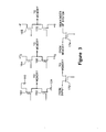
- Figure 3 illustrates generic FET switches 160-174, which may be any type of FET such JFET, MOSFET, P-Channel, N-Channel, etc. Such FET switches are faster, more reliable, and cheaper than mechanical switches. While FET switches are a good choice, again, other types of devices can also be used.
- switches 160 and 162 switch user ground 110 and earth ground 134
- switches 164 and 166 switch +F and +G
- switches 168 and 170 switch -F and-G
- switch 172 switches analog inputs to memory
- switch 174 switches the output of the memory to the remainder of the system.
- the driving of the FET switches is controlled by logic, such as from a processor (reference Figure 6 for a processor).
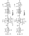
- Figure 4 depicts a high level block diagram of a signal acquisition system 200 according to a second embodiment of the present invention.
- the signal acquisition system 200 receives an input signal that is referenced to a user ground 210 on an input port 202.
- the input signal is amplified and/or otherwise processed by an analog network 204.
- the output of the analog network 204 is applied via a closed switch 206 to an analog fast-in-slow-out (FISO) memory 208.
- FISO fast-in-slow-out
- the FISO memory 208 is powered by +F and -F voltages from a floating power supply (which is not shown in Figure 4, but reference Figure 6) that is referenced to the user ground 210.
- the user ground 210 is also connected to the input port 202.
- the FISO memory 208 retains an analog version of the input signal.
- the output of the FISO memory 208 is applied to an open switch 212.
- the signal acquisition device 200 further includes an earth-referenced processor 230, which is connected to the switch 212, and a display 232.
- the earth-referenced processor 230 and the display 232 are referred to an earth ground 234 and are powered by +G and -G voltages from an earth-grounded power supply (which is not shown in Figure 4, but reference Figure 6).
- the devices that are continuously connected to the +G and -G voltages can be referred to as an instrumentation network.
- the +F voltage is connected to the FISO memory 208 via a switch 240
- the -F voltage is connected to the FISO memory 208 via a switch 242
- the user ground 210 is connected to the FISO memory 208 via a switch 244.
- the FISO memory 208 is electrically isolated from the Earth-referenced processor 230 and the display 232. Because the analog signal input on input port 202 is referenced to user ground 210 the input signal is not impacted by ground loops, high voltage differentials, noise, or other factors that might impact the earth ground 234.
- a set of switch-changes occurs. Specifically, the switch 206 opens, which disconnects the FISO memory 208 from the analog network 204. Additionally, the switch 244 switches the FISO memory 208 from the user ground 210 to the earth ground 234. At the same time, the switches 240 and 242 switch the FISO memory 208 from the +F and -F voltages to the +G and -G voltages. Finally, the switch 212 closes, connecting the FISO memory 208 to the earth-referenced processor 230.
- switches 240, 242, and 244 operate in a break-before-make fashion and all switches are beneficially high voltage analog (FET) switches (see Figure 3). If bipolar transistor switches are used DC level changes might have to be corrected for.
- FET high voltage analog
- Figures 1 through 5 illustrate generic signal acquisition systems 100 and 200 that can be used for many purposes in many different systems. However, such signal acquisition systems are particularly useful in oscilloscopes.
- Figure 6 illustrates a block diagram of an oscilloscope 600 that benefits from the principles of the present invention.
- the oscilloscope 600 includes an input 602 that is referenced to a user ground 604.
- a signal on the input 602 is passed to an acquisition system 606.
- the acquisition system 606 includes a user-selectable gain amplifier and an analog-to-digital converter (ADC).
- ADC analog-to-digital converter
- the ADC of the acquisition system 606 samples and quantizes the amplified signal and supplies the acquired information via closed switch 608 to an acquisition memory 610.
- the acquisition system 606 may store an analog representation of the input signal in a FISO memory.
- the oscilloscope 600 will be assumed to use an ADC and a digital memory.
- the acquisition memory 610 is powered by +F and -F voltages from a floating power supply 611 that is referenced to user ground 604.
- the +F and -F voltages are applied via switches 612 and 613, respectively, and the user ground 604 is applied by a switch 614.
- the acquisition system 606 is directly powered by the floating power supply 611 and is directly wired to the user ground 604.
- the output of the acquisition memory 610 is applied to a switch 615 which is open during data acquisition.
- a processor 616 causes the switch 608 to open and switch 615 to close. Contemporaneously, the processor 616 also causes switches 612, 613, and 614 to switch such that the acquisition memory 610 is powered by +G and -G voltage from an earth ground 617 power supply 618 and such that the acquisition memory 610 is connected to earth ground 617.
- the output of the acquisition memory 610 passes to a display memory 622 that stores the acquisition memory 610 output.
- the contents of the display memory 622 are employed to generate a waveform display on a raster scan display device 626.
- the processor 618 may provide additional information, such as the amplification factor and a waveform timebase to the display memory 622 for display.
- the processor 618 causes switch 615 to open and switch 608 to close. Additionally, the processor 618 causes switches 612, 613, and 614 to connect the acquisition memory 610 back to the floating power supply 611 voltages +F and -F and to the user ground 604.
- the earth grounded power supply 618 supplies power to the display 626, to the processor 618 and to the display memory 622. Furthermore, the processor 618 causes the various switches to switch in a break-before-make fashion. In one embodiment, instead of mechanical switches high-voltage FET switches are used (see Figure 3). All devices that are directly connected to the earth grounded power supply 618 and to earth ground 617 can be generically referred to as an instrumentation network.
Landscapes
- Physics & Mathematics (AREA)
- General Physics & Mathematics (AREA)
- Analogue/Digital Conversion (AREA)
- Electronic Switches (AREA)
- Tests Of Electronic Circuits (AREA)
- Recording Measured Values (AREA)
- Measurement Of Current Or Voltage (AREA)
Abstract
Description
- This patent application claims the benefit of U.S. Provisional Patent Application Serial Number 60/428,494, filed on November 22, 2002 and entitled, "MEANS FOR IMPLEMENTING ISOLATED CHANNELS," which is incorporated herein by reference in its entirety.
- The present invention relates generally to signal acquisition instruments and, more specifically, to signal acquisition instruments having isolated input channels.
- Modern signal acquisition instruments typically include an analog-input section for receiving signals being acquired, an analog processor such as an amplifier or filter, a digitization system for digitizing processed analog signals, and a memory for storing the digitized signals. For example, U.S. Patent No. 5,986,637, which issued to Etheridge et al. on November 16, 1999, describes a high speed digital storage oscilloscope (DSO) having such features.
- While generally successful, modern signal acquisition instruments can have problems in some applications, e.g., when acquiring signals from switched-mode power supplies, in locations with significant ground loops, or when small signals ride on large voltages. In such applications isolating the analog input stage so that it can utilize a user's ground can be beneficial. However, AC line-driven signal acquisition instruments typically must be electrically grounded relative to input AC power lines for safety and to comply with applicable electrical codes. Thus a conflict can exist between acquiring signals referenced to a user's ground and transferring the acquired information to the remainder of the signal acquisition instrument.
- One approach to transferring information acquired by an isolated input stage to the remainder of an AC powered system is to use optical, capacitive, and/or inductive coupling. While such coupling can transfer analog information across grounds, this approach has problems because the gain-bandwidth product of the coupler often must be high to maintain linearity, because feedback mechanisms are generally unreliable, and because data quality is problematic. Another approach is to use optical, capacitive, and/or inductive coupling to couple digitized signals from logic referenced to the user's ground to logic referenced to the instrument's ground. However, this approach is relatively costly and complex and can require a significant amount of power.
- Therefore, a new technique of coupling information gathered by an isolated input stage that is referenced to a user's ground to the remaining instrumentation that is referenced to instrument's ground would be beneficial.
- The principles of the present invention provide for architectures, apparatuses, and methods of coupling information acquired by an isolated input stage that is referenced to a user's ground to the remainder of the system instrumentation that is referenced to an earth ground (which typically connects to the ground line of AC input power). Those principles can be implemented by acquiring signal information using an isolated input stage that is referenced to a user's ground, storing the acquired information either in an analog format or a digital format in a storage element that is powered by a floating power supply that is referenced to the user's ground, disconnecting the storage element from the floating power and the user's ground, and then connecting the storage element to a power supply referenced to the earth ground. Because of their speed and high voltage-handling capability, FET switches are useful devices for connecting and disconnecting the storage element.
- In one embodiment of the invention, digital memory devices are used. In another embodiment analog memory, e.g., FISO (fast in-slow out) memory is used.
- The teachings of the present invention can be readily understood by considering the following detailed description in conjunction with the accompanying drawings, in which:
- Figure 1 depicts a high level block diagram of a signal acquisition system according to a first embodiment of the invention when that system is in a first state;
- Figure 2 depicts the signal acquisition system of Figure 1 when that system is in a second state;
- Figure 3 illustrates the use of FET switches;
- Figure 4 depicts a high level block diagram of a signal acquisition system according to another embodiment of the invention when that system is in a first state;
- Figure 5 depicts the signal acquisition system of Figure 4 when that system is in a second state; and
- Figure 6 depicts a block diagram of an oscilloscope that incorporates the principles of the present invention.
-
- To facilitate understanding, identical reference numerals have been used, where possible, to designate identical elements that are common to the figures.
- The subject invention will be primarily described within the context of a general signal acquisition instrument, and then in the context of a digital storage oscilloscopes (DSOs). It will be appreciated by those skilled in the art that the invention may be advantageously employed in many different systems where acquiring information referenced to one ground and then switching that information to another ground is desirable.
- Figure 1 depicts a high level block diagram of a
signal acquisition system 100 according to an embodiment of the present invention. Thesignal acquisition system 100 receives at aninput port 102 an input signal that is referenced to auser ground 110. The input signal is amplified and/or otherwise processed (e.g. filtered) by ananalog network 104. The output of theanalog network 104 is applied via a closedswitch 106 to adigitizer 108 that includes a memory. Thedigitizer 108 is powered by +F and -F voltages from a floating power supply (not shown in Figure 1, but see Figure 6 for such a power supply) that is referenced to theuser ground 110. - The
digitizer 108 converts the analog processed signal fromswitch 106 into digital values that are stored in its memory. At this time thedigitizer 108 output is applied to an open switch 112 (or switches). Thesignal acquisition device 100 further includes anearth ground 134 referencedprocessor 130, which is connected to theswitch 112, and anearth ground 134 referenceddisplay 132. Theprocessor 130 and thedisplay 132 are powered by voltages G+ and G- from an earth grounded referenced power supply (not shown in Figure 1, but see Figure 6 for such a power supply). For convenience all of the devices that are constantly powered by voltages G+ and G- can be generically referred to as an instrumentation network. Theearth ground 134 is, in one embodiment, connected to a ground input of AC input power. - As shown in Figure 1, the +F voltage is connected to the
digitizer 108 via aswitch 140, the -F voltage is connected to thedigitizer 108 via aswitch 142, and theuser ground 110 is connected to thedigitizer 108 via aswitch 144. Thus, in Figure 1 thedigitizer 108 is electrically isolated from the instrumentation network. Because theinput port 102 is referenced touser ground 110 the input signal is not impacted by ground loops, high voltage differential, noise, or other factors that impact theearth ground 134. For example, theearth ground 134 will usually be shared by other devices powered by a common AC power line, and those devices can produce ground loop voltage drops that will appear on theearth ground 134. - Referring now to Figure 2, after the
digitizer 108 has digitized the signal from theanalog network 104, a set of switch-changes occurs. Specifically, theswitch 106 opens, which disconnects thedigitizer 108 from theanalog network 104. Then, theswitch 144 disconnects thedigitizer 108 from theuser ground 110 and connects it to theearth ground 134, and theswitches digitizer 108 and connect thedigitizer 108 to the +G and -G. Finally, theswitch 112 closes, connecting thedigitizer 108 to theprocessor 130. - As shown in Figure 2, the
user ground 110 is no longer connected to thedigitizer 108. The switching ofuser ground 110 to earth-ground 134 is performed in a manner that avoids damage from differences between user and earth grounds, and thus possible damage to the input stage and/or the signal source while also providing thesignal acquisition system 100 with the protection afforded by a common earth ground. - It should be noted that in various embodiments switches 140, 142, and 144 operate in a break-before-make fashion. Furthermore, while the
switches switches switch user ground 110 andearth ground 134,switches switches switch 174 switches the output of the memory to the remainder of the system. The driving of the FET switches is controlled by logic, such as from a processor (reference Figure 6 for a processor). - While Figures 1 and 2 illustrate switching a
user ground 110 to earth-ground 134 after the acquired signal has been digitized, this is not required. Switching of analog signals is also possible. For example, Figure 4 depicts a high level block diagram of asignal acquisition system 200 according to a second embodiment of the present invention. Thesignal acquisition system 200 receives an input signal that is referenced to auser ground 210 on aninput port 202. The input signal is amplified and/or otherwise processed by ananalog network 204. The output of theanalog network 204 is applied via aclosed switch 206 to an analog fast-in-slow-out (FISO)memory 208. - As shown in Figure 4, the
FISO memory 208 is powered by +F and -F voltages from a floating power supply (which is not shown in Figure 4, but reference Figure 6) that is referenced to theuser ground 210. Theuser ground 210 is also connected to theinput port 202. TheFISO memory 208 retains an analog version of the input signal. The output of theFISO memory 208 is applied to anopen switch 212. Thesignal acquisition device 200 further includes an earth-referencedprocessor 230, which is connected to theswitch 212, and adisplay 232. The earth-referencedprocessor 230 and thedisplay 232 are referred to anearth ground 234 and are powered by +G and -G voltages from an earth-grounded power supply (which is not shown in Figure 4, but reference Figure 6). The devices that are continuously connected to the +G and -G voltages can be referred to as an instrumentation network. - As shown in Figure 4, the +F voltage is connected to the
FISO memory 208 via aswitch 240, the -F voltage is connected to theFISO memory 208 via aswitch 242, and theuser ground 210 is connected to theFISO memory 208 via aswitch 244. Thus, in Figure 4 theFISO memory 208 is electrically isolated from the Earth-referencedprocessor 230 and thedisplay 232. Because the analog signal input oninput port 202 is referenced touser ground 210 the input signal is not impacted by ground loops, high voltage differentials, noise, or other factors that might impact theearth ground 234. - Referring now to Figure 5, after the
FISO memory 208 has captured the signal from theanalog network 204, a set of switch-changes occurs. Specifically, theswitch 206 opens, which disconnects theFISO memory 208 from theanalog network 204. Additionally, theswitch 244 switches theFISO memory 208 from theuser ground 210 to theearth ground 234. At the same time, theswitches FISO memory 208 from the +F and -F voltages to the +G and -G voltages. Finally, theswitch 212 closes, connecting theFISO memory 208 to the earth-referencedprocessor 230. - As in the embodiments illustrated in Figures 1 and 2, the
switches - Figures 1 through 5 illustrate generic
signal acquisition systems oscilloscope 600 that benefits from the principles of the present invention. As shown, theoscilloscope 600 includes aninput 602 that is referenced to auser ground 604. A signal on theinput 602 is passed to anacquisition system 606. Theacquisition system 606 includes a user-selectable gain amplifier and an analog-to-digital converter (ADC). The ADC of theacquisition system 606 samples and quantizes the amplified signal and supplies the acquired information viaclosed switch 608 to anacquisition memory 610. It is also possible for theacquisition system 606 to store an analog representation of the input signal in a FISO memory. However, for convenience, theoscilloscope 600 will be assumed to use an ADC and a digital memory. During data acquisition, and as shown in Figure 6, theacquisition memory 610 is powered by +F and -F voltages from a floatingpower supply 611 that is referenced touser ground 604. The +F and -F voltages are applied viaswitches user ground 604 is applied by aswitch 614. It should be understood that theacquisition system 606 is directly powered by the floatingpower supply 611 and is directly wired to theuser ground 604. The output of theacquisition memory 610 is applied to aswitch 615 which is open during data acquisition. - After data acquisition is complete, a processor 616 causes the
switch 608 to open and switch 615 to close. Contemporaneously, the processor 616 also causesswitches acquisition memory 610 is powered by +G and -G voltage from anearth ground 617power supply 618 and such that theacquisition memory 610 is connected toearth ground 617. - With
switch 615 closed, the output of theacquisition memory 610 passes to adisplay memory 622 that stores theacquisition memory 610 output. The contents of thedisplay memory 622 are employed to generate a waveform display on a rasterscan display device 626. Theprocessor 618 may provide additional information, such as the amplification factor and a waveform timebase to thedisplay memory 622 for display. After thedisplay memory 622 has stored the output of theacquisition memory 610 theprocessor 618 causes switch 615 to open and switch 608 to close. Additionally, theprocessor 618causes switches acquisition memory 610 back to the floatingpower supply 611 voltages +F and -F and to theuser ground 604. It should be understood that the earth groundedpower supply 618 supplies power to thedisplay 626, to theprocessor 618 and to thedisplay memory 622. Furthermore, theprocessor 618 causes the various switches to switch in a break-before-make fashion. In one embodiment, instead of mechanical switches high-voltage FET switches are used (see Figure 3). All devices that are directly connected to the earth groundedpower supply 618 and toearth ground 617 can be generically referred to as an instrumentation network. - While the foregoing is directed to the preferred embodiment of the present invention, other and further embodiments of the invention may be devised without departing from the basic scope thereof, and the scope thereof is determined by the claims that follow.
Claims (20)
- A signal acquisition instrument, comprising:wherein said first and second grounds are electrically isolated.an input stage referenced to a first ground, said input stage for receiving an input signal;a memory for storing information related to said input signal;an instrumentation network referenced to a second ground, said instrumentation network for processing information from said memory; anda switch network having at least two switches for selectively switching said memory between said first and second grounds;
- The signal acquisition instrument of claim 1 wherein said switch network includes at least one semiconductor switch.
- The signal acquisition instrument of claim 1 wherein at least one switch is a break-before-make switch.
- The signal acquisition instrument of claim 1 wherein said switch network selectively connects said memory to said input stage.
- The signal acquisition instrument of claim 1 wherein said switch network selectively connects said memory to said instrumentation network.
- The signal acquisition instrument of claim 1 wherein said memory is a digital memory.
- The signal acquisition instrument of claim 1 wherein said memory is an analog memory.
- The signal acquisition instrument of claim 1 wherein said an instrument network includes a display.
- The signal acquisition instrument of claim 1 wherein said second ground is electrically connected to an AC power ground line.
- An oscilloscope, comprising:wherein said first and second grounds are electrically isolated.an input stage referenced to a first ground, said input stage for receiving an input signal;a memory for storing information related to said input signal;an instrumentation network referenced to a second ground, said instrumentation network for processing information from said memory;a display for displaying a waveform representation of said input signal; anda switch network having at least two switches for selectively switching said memory between said first ground and said second ground;
- The oscilloscope of claim 10 wherein said switch network includes at least one semiconductor switch.
- The oscilloscope of claim 10 wherein at least one switch is a break-before-make switch.
- The oscilloscope of claim 10 wherein said switch network selectively connects said memory to said input stage.
- The oscilloscope of claim 10 wherein said switch network selectively connects said memory to said instrumentation network.
- The oscilloscope of claim 10 wherein said memory is a digital memory.
- The oscilloscope of claim 10 wherein said memory is an analog memory.
- The oscilloscope of claim 10 wherein said oscilloscope is a digital storage oscilloscope.
- The oscilloscope of claim 10 wherein said second ground is electrically connected to an AC power ground line.
- A method of acquiring a signal comprising:receiving a signal referenced to a first ground;storing information about the received signal in a memory referenced to the first ground;disconnecting the memory from the first ground;referencing the memory to a second ground; andprocessing the stored information using a system referenced to the second ground.
- The method of claim 19 further including the step of displaying a waveform representation of the received signal.
Applications Claiming Priority (2)
| Application Number | Priority Date | Filing Date | Title |
|---|---|---|---|
| US42849402P | 2002-11-22 | 2002-11-22 | |
| US428494P | 2002-11-22 |
Publications (2)
| Publication Number | Publication Date |
|---|---|
| EP1422531A1 true EP1422531A1 (en) | 2004-05-26 |
| EP1422531B1 EP1422531B1 (en) | 2006-03-01 |
Family
ID=32230434
Family Applications (1)
| Application Number | Title | Priority Date | Filing Date |
|---|---|---|---|
| EP03257167A Expired - Lifetime EP1422531B1 (en) | 2002-11-22 | 2003-11-13 | Measurement channel isolation by switching between different grounds |
Country Status (5)
| Country | Link |
|---|---|
| US (1) | US6944559B2 (en) |
| EP (1) | EP1422531B1 (en) |
| JP (1) | JP4204954B2 (en) |
| CN (1) | CN100350255C (en) |
| DE (1) | DE60303760T2 (en) |
Cited By (2)
| Publication number | Priority date | Publication date | Assignee | Title |
|---|---|---|---|---|
| FR2870939A1 (en) * | 2004-05-27 | 2005-12-02 | Chauvin Arnoux | MULTIVOIC DIGITAL OSCILLOSCOPES |
| CN102269619A (en) * | 2011-05-16 | 2011-12-07 | 杭州电子科技大学 | Wireless sensor network-based acoustic signal acquisition terminal |
Families Citing this family (2)
| Publication number | Priority date | Publication date | Assignee | Title |
|---|---|---|---|---|
| US8410804B1 (en) * | 2009-02-24 | 2013-04-02 | Keithley Instruments, Inc. | Measurement system with high frequency ground switch |
| US8760000B2 (en) | 2010-11-19 | 2014-06-24 | Honeywell International Inc. | Mixed signal conversion, isolation, and transmission for aerospace multi-channel data and power interface systems |
Citations (3)
| Publication number | Priority date | Publication date | Assignee | Title |
|---|---|---|---|---|
| US4876520A (en) * | 1987-07-30 | 1989-10-24 | Hewlett-Packard Company | Coaxial switching system with switched shields and crosstalk suppression |
| DE4314484A1 (en) * | 1993-05-03 | 1994-11-10 | Metrawatt Gmbh Gossen | Data acquisition for use with a mobile electronic multimeter, especially a handheld multimeter |
| US5986637A (en) * | 1994-04-13 | 1999-11-16 | Tektronix, Inc. | Digital oscilloscope architecture for signal monitoring with enhanced duty cycle |
Family Cites Families (14)
| Publication number | Priority date | Publication date | Assignee | Title |
|---|---|---|---|---|
| US4375660A (en) * | 1981-02-03 | 1983-03-01 | Tektronix, Inc. | Ground isolation monitoring apparatus having a protective circuit |
| US4940931A (en) * | 1988-06-24 | 1990-07-10 | Anritsu Corporation | Digital waveform measuring apparatus having a shading-tone display function |
| US5250893A (en) * | 1992-01-31 | 1993-10-05 | Tegam, Inc. | Digital voltmeter |
| US5379176A (en) * | 1993-05-03 | 1995-01-03 | John Fluke Mfg. Co., Inc. | Protective input circuit for an instrument |
| US5517154A (en) * | 1995-01-13 | 1996-05-14 | Tektronix, Inc. | Split-path linear isolation circuit apparatus and method |
| US5594329A (en) * | 1995-09-11 | 1997-01-14 | Fluke Corporation | Method and apparatus for obtaining voltage-isolated measurement channels with an isolation transformer and multiplier |
| US5717154A (en) * | 1996-03-25 | 1998-02-10 | Advanced Micro Devices, Inc. | Computer system and method for performing wavetable music synthesis which stores wavetable data in system memory employing a high priority I/O bus request mechanism for improved audio fidelity |
| US5834973A (en) * | 1997-05-01 | 1998-11-10 | Fluke Corporation | Voltage isolation circuit for a measurement channel |
| US6278596B1 (en) * | 1999-06-17 | 2001-08-21 | Tektronix, Inc. | Active ground fault disconnect |
| US6487456B1 (en) * | 2000-02-11 | 2002-11-26 | Thomas Michael Masano | Method and apparatus for creating a selectable electrical characteristic |
| US6538420B2 (en) * | 2001-04-10 | 2003-03-25 | Associated Research, Inc. | Automated run test system having built-in high voltage switching matrix for interconnection to a safety compliance testing instrument |
| EP1335207B1 (en) * | 2002-02-11 | 2012-10-10 | Tektronix, Inc. | Method and device for capturing a signal |
| US7113750B2 (en) * | 2002-12-16 | 2006-09-26 | Tektronix, Inc. | Apparatus and method for input channel isolation within an electronic test instrument |
| US20040162694A1 (en) * | 2003-02-13 | 2004-08-19 | Ricca Paolo Dalla | Programmable digital interface for analog test equipment systems |
-
2003
- 2003-09-12 US US10/661,309 patent/US6944559B2/en not_active Expired - Fee Related
- 2003-11-13 DE DE60303760T patent/DE60303760T2/en not_active Expired - Fee Related
- 2003-11-13 EP EP03257167A patent/EP1422531B1/en not_active Expired - Lifetime
- 2003-11-19 JP JP2003389237A patent/JP4204954B2/en not_active Expired - Fee Related
- 2003-11-21 CN CNB2003101231804A patent/CN100350255C/en not_active Expired - Fee Related
Patent Citations (3)
| Publication number | Priority date | Publication date | Assignee | Title |
|---|---|---|---|---|
| US4876520A (en) * | 1987-07-30 | 1989-10-24 | Hewlett-Packard Company | Coaxial switching system with switched shields and crosstalk suppression |
| DE4314484A1 (en) * | 1993-05-03 | 1994-11-10 | Metrawatt Gmbh Gossen | Data acquisition for use with a mobile electronic multimeter, especially a handheld multimeter |
| US5986637A (en) * | 1994-04-13 | 1999-11-16 | Tektronix, Inc. | Digital oscilloscope architecture for signal monitoring with enhanced duty cycle |
Non-Patent Citations (1)
| Title |
|---|
| SEKEL STEVE: "Making oscilloscope measurements more accurate, less likely to shock", R&D MAGAZINE, October 1995 (1995-10-01), XP001090956 * |
Cited By (3)
| Publication number | Priority date | Publication date | Assignee | Title |
|---|---|---|---|---|
| FR2870939A1 (en) * | 2004-05-27 | 2005-12-02 | Chauvin Arnoux | MULTIVOIC DIGITAL OSCILLOSCOPES |
| WO2005119273A1 (en) * | 2004-05-27 | 2005-12-15 | Chauvin Arnoux | Multi-channel digital oscilloscope |
| CN102269619A (en) * | 2011-05-16 | 2011-12-07 | 杭州电子科技大学 | Wireless sensor network-based acoustic signal acquisition terminal |
Also Published As
| Publication number | Publication date |
|---|---|
| CN100350255C (en) | 2007-11-21 |
| US20040102909A1 (en) | 2004-05-27 |
| CN1515910A (en) | 2004-07-28 |
| JP2004177406A (en) | 2004-06-24 |
| DE60303760D1 (en) | 2006-04-27 |
| JP4204954B2 (en) | 2009-01-07 |
| US6944559B2 (en) | 2005-09-13 |
| EP1422531B1 (en) | 2006-03-01 |
| DE60303760T2 (en) | 2006-09-28 |
Similar Documents
| Publication | Publication Date | Title |
|---|---|---|
| US20110080925A1 (en) | Low power, high speed multi-channel data acquisition system and method | |
| KR101727083B1 (en) | Mixed signal acquisition system for a measurement instrument | |
| US5410363A (en) | Automatic gain control device for transmitting video signals between two locations by use of a known reference pulse during vertical blanking period so as to control the gain of the video signals at the second location | |
| US12590996B2 (en) | Systems, devices, and methods for measuring direct current/low frequency signal components | |
| EP1069739A3 (en) | Removal of a common mode voltage in a differential receiver | |
| US20050140388A1 (en) | Hybrid AC/DC-coupled channel for testing | |
| US20180284159A1 (en) | Current measurement techniques to compensate for shunt drift | |
| WO2008022251A2 (en) | Multiple probe acquisition system | |
| EP1422531B1 (en) | Measurement channel isolation by switching between different grounds | |
| EP3776863B1 (en) | Floating input detection | |
| JP2001007660A (en) | Analog signal processing circuit, AD converter, semiconductor device tester, and oscilloscope | |
| EP1335208B1 (en) | Method and apparatus for the digital and analog triggering | |
| US7308519B2 (en) | Communications bus management circuit | |
| AU2014203115A1 (en) | Multiple bipolar sampling | |
| CN121039506A (en) | Test and measurement instruments with integrated analog front end | |
| US8233643B1 (en) | System and method for amplifying low level signals provided on electrical supply power | |
| JP2932044B2 (en) | Signal conditioning circuit | |
| US6744391B2 (en) | System for sampling a signal in an electronic instrument using a unipolar A/D converter | |
| US20260029431A1 (en) | Optical Probing System with Multi-Signal Modulation and Demodulation | |
| JP2001339256A (en) | Switching type AC signal amplifier | |
| US20100127750A1 (en) | Switched capacitor input stage for imaging front-ends | |
| JP3002550B2 (en) | Automatic synchronization signal polarity conversion circuit for monitor device | |
| Huang et al. | A Generic Isolated Energy Probe for High-Side Switching Loss Measurement | |
| RU2053710C1 (en) | Multichannel biopotential amplifier | |
| CN118017999A (en) | Isolation conversion circuit and system |
Legal Events
| Date | Code | Title | Description |
|---|---|---|---|
| PUAI | Public reference made under article 153(3) epc to a published international application that has entered the european phase |
Free format text: ORIGINAL CODE: 0009012 |
|
| AK | Designated contracting states |
Kind code of ref document: A1 Designated state(s): AT BE BG CH CY CZ DE DK EE ES FI FR GB GR HU IE IT LI LU MC NL PT RO SE SI SK TR |
|
| AX | Request for extension of the european patent |
Extension state: AL LT LV MK |
|
| 17P | Request for examination filed |
Effective date: 20041123 |
|
| AKX | Designation fees paid |
Designated state(s): DE FR GB IT |
|
| GRAP | Despatch of communication of intention to grant a patent |
Free format text: ORIGINAL CODE: EPIDOSNIGR1 |
|
| GRAS | Grant fee paid |
Free format text: ORIGINAL CODE: EPIDOSNIGR3 |
|
| GRAA | (expected) grant |
Free format text: ORIGINAL CODE: 0009210 |
|
| AK | Designated contracting states |
Kind code of ref document: B1 Designated state(s): DE FR GB IT |
|
| PG25 | Lapsed in a contracting state [announced via postgrant information from national office to epo] |
Ref country code: IT Free format text: LAPSE BECAUSE OF FAILURE TO SUBMIT A TRANSLATION OF THE DESCRIPTION OR TO PAY THE FEE WITHIN THE PRESCRIBED TIME-LIMIT;WARNING: LAPSES OF ITALIAN PATENTS WITH EFFECTIVE DATE BEFORE 2007 MAY HAVE OCCURRED AT ANY TIME BEFORE 2007. THE CORRECT EFFECTIVE DATE MAY BE DIFFERENT FROM THE ONE RECORDED. Effective date: 20060301 |
|
| REG | Reference to a national code |
Ref country code: GB Ref legal event code: FG4D |
|
| REF | Corresponds to: |
Ref document number: 60303760 Country of ref document: DE Date of ref document: 20060427 Kind code of ref document: P |
|
| ET | Fr: translation filed | ||
| PLBE | No opposition filed within time limit |
Free format text: ORIGINAL CODE: 0009261 |
|
| STAA | Information on the status of an ep patent application or granted ep patent |
Free format text: STATUS: NO OPPOSITION FILED WITHIN TIME LIMIT |
|
| 26N | No opposition filed |
Effective date: 20061204 |
|
| PGFP | Annual fee paid to national office [announced via postgrant information from national office to epo] |
Ref country code: DE Payment date: 20081119 Year of fee payment: 6 |
|
| PGFP | Annual fee paid to national office [announced via postgrant information from national office to epo] |
Ref country code: IT Payment date: 20081020 Year of fee payment: 6 |
|
| PGFP | Annual fee paid to national office [announced via postgrant information from national office to epo] |
Ref country code: FR Payment date: 20081013 Year of fee payment: 6 |
|
| PGFP | Annual fee paid to national office [announced via postgrant information from national office to epo] |
Ref country code: GB Payment date: 20081022 Year of fee payment: 6 |
|
| GBPC | Gb: european patent ceased through non-payment of renewal fee |
Effective date: 20091113 |
|
| REG | Reference to a national code |
Ref country code: FR Ref legal event code: ST Effective date: 20100730 |
|
| PG25 | Lapsed in a contracting state [announced via postgrant information from national office to epo] |
Ref country code: FR Free format text: LAPSE BECAUSE OF NON-PAYMENT OF DUE FEES Effective date: 20091130 |
|
| PG25 | Lapsed in a contracting state [announced via postgrant information from national office to epo] |
Ref country code: DE Free format text: LAPSE BECAUSE OF NON-PAYMENT OF DUE FEES Effective date: 20100601 |
|
| PG25 | Lapsed in a contracting state [announced via postgrant information from national office to epo] |
Ref country code: GB Free format text: LAPSE BECAUSE OF NON-PAYMENT OF DUE FEES Effective date: 20091113 |
|
| PG25 | Lapsed in a contracting state [announced via postgrant information from national office to epo] |
Ref country code: IT Free format text: LAPSE BECAUSE OF NON-PAYMENT OF DUE FEES Effective date: 20091113 |