EP1417521B1 - Optische filter, ihre herstellungsverfahren und ihre anwendung für ein multiplexsystem - Google Patents
Optische filter, ihre herstellungsverfahren und ihre anwendung für ein multiplexsystem Download PDFInfo
- Publication number
- EP1417521B1 EP1417521B1 EP01976412A EP01976412A EP1417521B1 EP 1417521 B1 EP1417521 B1 EP 1417521B1 EP 01976412 A EP01976412 A EP 01976412A EP 01976412 A EP01976412 A EP 01976412A EP 1417521 B1 EP1417521 B1 EP 1417521B1
- Authority
- EP
- European Patent Office
- Prior art keywords
- component according
- thin film
- grating
- features
- component
- Prior art date
- Legal status (The legal status is an assumption and is not a legal conclusion. Google has not performed a legal analysis and makes no representation as to the accuracy of the status listed.)
- Expired - Lifetime
Links
Images


Classifications
-
- G—PHYSICS
- G02—OPTICS
- G02B—OPTICAL ELEMENTS, SYSTEMS OR APPARATUS
- G02B6/00—Light guides; Structural details of arrangements comprising light guides and other optical elements, e.g. couplings
- G02B6/24—Coupling light guides
- G02B6/26—Optical coupling means
- G02B6/28—Optical coupling means having data bus means, i.e. plural waveguides interconnected and providing an inherently bidirectional system by mixing and splitting signals
- G02B6/293—Optical coupling means having data bus means, i.e. plural waveguides interconnected and providing an inherently bidirectional system by mixing and splitting signals with wavelength selective means
- G02B6/29304—Optical coupling means having data bus means, i.e. plural waveguides interconnected and providing an inherently bidirectional system by mixing and splitting signals with wavelength selective means operating by diffraction, e.g. grating
- G02B6/29305—Optical coupling means having data bus means, i.e. plural waveguides interconnected and providing an inherently bidirectional system by mixing and splitting signals with wavelength selective means operating by diffraction, e.g. grating as bulk element, i.e. free space arrangement external to a light guide
- G02B6/2931—Diffractive element operating in reflection
-
- G—PHYSICS
- G02—OPTICS
- G02B—OPTICAL ELEMENTS, SYSTEMS OR APPARATUS
- G02B6/00—Light guides; Structural details of arrangements comprising light guides and other optical elements, e.g. couplings
- G02B6/10—Light guides; Structural details of arrangements comprising light guides and other optical elements, e.g. couplings of the optical waveguide type
- G02B6/12—Light guides; Structural details of arrangements comprising light guides and other optical elements, e.g. couplings of the optical waveguide type of the integrated circuit kind
- G02B6/12007—Light guides; Structural details of arrangements comprising light guides and other optical elements, e.g. couplings of the optical waveguide type of the integrated circuit kind forming wavelength selective elements, e.g. multiplexer, demultiplexer
-
- G—PHYSICS
- G02—OPTICS
- G02B—OPTICAL ELEMENTS, SYSTEMS OR APPARATUS
- G02B6/00—Light guides; Structural details of arrangements comprising light guides and other optical elements, e.g. couplings
- G02B6/10—Light guides; Structural details of arrangements comprising light guides and other optical elements, e.g. couplings of the optical waveguide type
- G02B6/12—Light guides; Structural details of arrangements comprising light guides and other optical elements, e.g. couplings of the optical waveguide type of the integrated circuit kind
- G02B6/122—Basic optical elements, e.g. light-guiding paths
- G02B6/124—Geodesic lenses or integrated gratings
-
- G—PHYSICS
- G02—OPTICS
- G02B—OPTICAL ELEMENTS, SYSTEMS OR APPARATUS
- G02B6/00—Light guides; Structural details of arrangements comprising light guides and other optical elements, e.g. couplings
- G02B6/24—Coupling light guides
- G02B6/26—Optical coupling means
- G02B6/28—Optical coupling means having data bus means, i.e. plural waveguides interconnected and providing an inherently bidirectional system by mixing and splitting signals
- G02B6/293—Optical coupling means having data bus means, i.e. plural waveguides interconnected and providing an inherently bidirectional system by mixing and splitting signals with wavelength selective means
- G02B6/29304—Optical coupling means having data bus means, i.e. plural waveguides interconnected and providing an inherently bidirectional system by mixing and splitting signals with wavelength selective means operating by diffraction, e.g. grating
- G02B6/29305—Optical coupling means having data bus means, i.e. plural waveguides interconnected and providing an inherently bidirectional system by mixing and splitting signals with wavelength selective means operating by diffraction, e.g. grating as bulk element, i.e. free space arrangement external to a light guide
- G02B6/29311—Diffractive element operating in transmission
-
- G—PHYSICS
- G02—OPTICS
- G02B—OPTICAL ELEMENTS, SYSTEMS OR APPARATUS
- G02B6/00—Light guides; Structural details of arrangements comprising light guides and other optical elements, e.g. couplings
- G02B6/24—Coupling light guides
- G02B6/26—Optical coupling means
- G02B6/28—Optical coupling means having data bus means, i.e. plural waveguides interconnected and providing an inherently bidirectional system by mixing and splitting signals
- G02B6/293—Optical coupling means having data bus means, i.e. plural waveguides interconnected and providing an inherently bidirectional system by mixing and splitting signals with wavelength selective means
- G02B6/29379—Optical coupling means having data bus means, i.e. plural waveguides interconnected and providing an inherently bidirectional system by mixing and splitting signals with wavelength selective means characterised by the function or use of the complete device
- G02B6/2938—Optical coupling means having data bus means, i.e. plural waveguides interconnected and providing an inherently bidirectional system by mixing and splitting signals with wavelength selective means characterised by the function or use of the complete device for multiplexing or demultiplexing, i.e. combining or separating wavelengths, e.g. 1xN, NxM
-
- G—PHYSICS
- G02—OPTICS
- G02B—OPTICAL ELEMENTS, SYSTEMS OR APPARATUS
- G02B6/00—Light guides; Structural details of arrangements comprising light guides and other optical elements, e.g. couplings
- G02B6/10—Light guides; Structural details of arrangements comprising light guides and other optical elements, e.g. couplings of the optical waveguide type
- G02B6/12—Light guides; Structural details of arrangements comprising light guides and other optical elements, e.g. couplings of the optical waveguide type of the integrated circuit kind
- G02B2006/12083—Constructional arrangements
- G02B2006/12107—Grating
-
- G—PHYSICS
- G02—OPTICS
- G02B—OPTICAL ELEMENTS, SYSTEMS OR APPARATUS
- G02B6/00—Light guides; Structural details of arrangements comprising light guides and other optical elements, e.g. couplings
- G02B6/24—Coupling light guides
- G02B6/26—Optical coupling means
- G02B6/28—Optical coupling means having data bus means, i.e. plural waveguides interconnected and providing an inherently bidirectional system by mixing and splitting signals
- G02B6/293—Optical coupling means having data bus means, i.e. plural waveguides interconnected and providing an inherently bidirectional system by mixing and splitting signals with wavelength selective means
- G02B6/29346—Optical coupling means having data bus means, i.e. plural waveguides interconnected and providing an inherently bidirectional system by mixing and splitting signals with wavelength selective means operating by wave or beam interference
- G02B6/29361—Interference filters, e.g. multilayer coatings, thin film filters, dichroic splitters or mirrors based on multilayers, WDM filters
- G02B6/29362—Serial cascade of filters or filtering operations, e.g. for a large number of channels
- G02B6/29365—Serial cascade of filters or filtering operations, e.g. for a large number of channels in a multireflection configuration, i.e. beam following a zigzag path between filters or filtering operations
-
- G—PHYSICS
- G02—OPTICS
- G02F—OPTICAL DEVICES OR ARRANGEMENTS FOR THE CONTROL OF LIGHT BY MODIFICATION OF THE OPTICAL PROPERTIES OF THE MEDIA OF THE ELEMENTS INVOLVED THEREIN; NON-LINEAR OPTICS; FREQUENCY-CHANGING OF LIGHT; OPTICAL LOGIC ELEMENTS; OPTICAL ANALOGUE/DIGITAL CONVERTERS
- G02F2201/00—Constructional arrangements not provided for in groups G02F1/00 - G02F7/00
- G02F2201/30—Constructional arrangements not provided for in groups G02F1/00 - G02F7/00 grating
- G02F2201/307—Reflective grating, i.e. Bragg grating
-
- G—PHYSICS
- G02—OPTICS
- G02F—OPTICAL DEVICES OR ARRANGEMENTS FOR THE CONTROL OF LIGHT BY MODIFICATION OF THE OPTICAL PROPERTIES OF THE MEDIA OF THE ELEMENTS INVOLVED THEREIN; NON-LINEAR OPTICS; FREQUENCY-CHANGING OF LIGHT; OPTICAL LOGIC ELEMENTS; OPTICAL ANALOGUE/DIGITAL CONVERTERS
- G02F2203/00—Function characteristic
- G02F2203/05—Function characteristic wavelength dependent
- G02F2203/055—Function characteristic wavelength dependent wavelength filtering
Definitions
- the present invention relates to an optical filter, to its manufacturing method and its use for a multiplex system optical wavelength division.
- the technical field of the invention is that of the manufacture of optical fiber telecommunications systems.
- WDM system for "Wavelength Division Multiplex”
- WDM system for "Wavelength Division Multiplex”
- WDM system for "Wavelength Division Multiplex”
- US Patent 5,216,680 discloses a mathematical method of resonance phenomena analysis in a waveguide and suggests applying the results to the design of an optical filter resonant for laser, but without describing the filter; the US patent 6,035, 089 states that this method can be used to design a filter consisting of strips dug into a supported waveguide by a substrate, then filled with a material suitable for obtaining a structure resonant, particularly at 533.4 nm.
- the present invention aims to provide an optical filter improved, a multiplexer (and a demultiplexer) incorporating this filter, and its manufacturing process.
- An object of the invention is to remedy, in part at least, the disadvantages of known optical filters and their manufacturing.
- structures are resonant at a certain wavelength and under an impact determined; resonance is achieved by building a network patterns on the surface and where appropriate in the thickness of at least one waveguide constituted by a thin layer or a stack of thin layers; the resonance results from an electromagnetic coupling by the network between an incident wave substantially according to the normal to the surface of the waveguide (and / or thin layers), and a mode guided waveguide: the resonance is observed when temporal and spatial frequencies of the incident wave are substantially equal to those corresponding to an eigenmode of the structure;
- patterns are generally provided whose dimensions and the spacing are close to the desired wavelength, and generally lower than this.
- said structure and / or said network is biperiodic or pluriperiodic: it (it) comprises a plurality of identical first patterns, regularly spaced according to two directions parallel to the waveguide, and according to a first step; it (it) further comprises a plurality of second identical patterns which are regularly spaced along the said directions and according to first step, which are arranged nested with said first patterns and which are of different shape, configuration and / or dimensions of those of the first motives.
- said first patterns form a first "subnet” that is nested with a second "subnet Constituted by said second patterns.
- the resonant network may comprise more than two subnets, especially 3 or 4 nested subnets to form the pluriperiodic (or multiperiodic) network.
- Such a structure makes it possible to provide bandpass filtering in reflection, which has a high rejection rate and allows tilt (usually low value) of the incident wave by normal to the surface of the thin layers of the waveguide, this inclination being desirable to separate the reflected beam from the incident beam, without requiring the use of a semi-reflective blade or an interferential system.
- Such a structure makes it possible to obtain improved performances for variations in the angle of incidence, the opening angle, or polarization of the incident beam.
- a component is used optical system comprising several thin layers superimposed on a substrate and incorporating two such resonant structures, which are of preferably arranged symmetrically with respect to a median plane, and which are identical and / or resonant at the same wavelength; we thus obtains a passband passive passover filter which is endowed a high rejection rate, and which is simple to manufacture.
- a network of protruding patterns in the form of studs can be obtained by etching a thin layer by an electron beam and / or by microlithography (or equivalent process).
- each of the patterns consists of (or has a) thin-film region of which the index is modified locally by the implantation of ions in the layer slim ; this implantation is obtained by subjecting the thin layer to ion bombardment, by an ion beam delivered by a particle accelerator, ion gun and / or ionic implant.
- This implantation operation uses a known technique especially for doping a semiconductor material with materials dopants.
- doping material a material selected from erbium, niobium, titanium, silicon, phosphorus or germanium.
- a technique of masking of the thin layer such as that used for etching: we cover the thin layer to be doped with a "perforated" shape mask complementary to that of the network of patterns to be formed; The mask thus prevents the parts of the thin layer that it covers from be subject to ionic flux; so it allows preservation, in the thin layer that it covers, undoped areas surrounding the regions doped.
- the ion configuration of the doped units can be varied by particular the density of implanted ions and / or the depth in order to obtain a configuration of shape (profile) and / or determined index.
- a structure annealing after doping can be carried out to modify, in a controlled way, by migration of ions in the layer thin, the gradient index and / or ionic population in the patterns doped.
- the realization of a component incorporating two networks resonant can be performed by engraving (or implanting) both networks on two portions of a thin layer resting on a substrate common ; the substrate can then be cut into two parts that can be assembled to form the component; assembly can be made by contacting the two parts by the face on which is the network; this assembly can be obtained by molecular adhesion; alternatively the two parts can be assembled by their respective portions of the substrate, if appropriate by gluing.
- an etching can be carried out (or doping) on the surface of each of two stacks of layers provided on each of the two faces of a substrate common to two stacks.
- the network is etched (or implanted) in a anti-reflective structure comprising at least one thin layer.
- Improved performance are obtained by forming (engraving or implanting) the patterns of each network in a so-called external layer of index (for example neighbor of 1.5) lower than that (for example close to 2) of the layer on which the outer layer is deposited, which leads to a anti-reflective structure.
- a so-called external layer of index for example neighbor of 1.5
- the components according to the invention have the advantage of require a reduced number of thin layers, compared with conventional thin film filters.
- two or three thin layers may be sufficient to construct a bandpass filter with a high rejection for wavelengths far from the length on which the filter is centered, having a spectral width less than one nanometer and reflecting or transmitting about 100 % of the incident beam - outside the bandwidth - even when the incident beam has an incidence (relative to the normal degree) and / or an opening of a few mrd, especially 5 to 20 mrd.
- the position of the central wavelength is basically determined by the geometry of the network that spans the external face (s) of the component, it is easy to shift and / or to adjust the central wavelength after realization of the network: this in particular can be obtained by covering the network with a thin layer of suitable index and thickness, or by modifying the network geometry, for example by a later step of etching by electron beam.
- Thin layers (inactive) can be produced by depositing a material chosen from metals such as Al, Ni, Ag, Au, oxides such as TiO 2 , SiO 2 , Ta 2 O 5 , fluorides (such as MgF 2 ), sulphides (such as Z n S) or nitrides; each thin layer has a thickness generally ranging from 10 nm to 10 ⁇ m; the thickness of the thin layer covering the network to shift the central wavelength may be less than these values: it can range from 1 to 10 nm (nanometer).
- the substrate has a greater thickness, for example of the order of 0.5 mm to 1 mm; it consists of a material transparent for the wavelengths considered, in particular the wavelengths close to 1.5 ⁇ m, such as glass or silica.
- the etching of the network can be obtained by various techniques, such as the technique of dry etching, wet etching, etching reactive, ion beam-etching, where appropriate assisted chemically.
- a filter thin layers in which at least one of the thin layers, so-called active layer, is made of a non-amorphous material; index and / or the geometry of this layer can be substantially reversibly modified when placed in a field electrical, especially when crossed by a current electric.
- Said material is furthermore transparent to the wavelengths of particularly in the infrared field, particularly in wavelengths close to 1.5 micron.
- the constituent material of said active layer can be essentially crystalline; however, in many cases this material is partially crystalline.
- this material may have properties of the materials conductors or semiconductors, it will in many cases have properties of electrically insulating materials.
- Said active thin layer may in particular be made by depositing a material selected from LiNbO 3 , BaTiO 3 , ZnO; this layer can also be made by depositing other materials usually used for the manufacture of thin layers; however, in order not to obtain an amorphous structure resulting from the usual deposition techniques of these materials, it is necessary to modify the deposition process to obtain a partially crystalline layer; especially when Ta 2 O 5 is used , the deposition can be brought to a temperature above the usual temperature; in particular, it is possible to operate at a temperature ranging from 200 or 300 ° C. to 800 or 900 ° C., rather than operating at the usual temperatures which are generally less than or equal to 100 ° C.
- said active layer partially at least crystalline, is the one in which are formed the motives of the network; thus, the small amplitude modification, the index and / or dimensions of this layer causes a displacement the center frequency of the filter.
- the layer filter Thin may have two active thin layers extending from and another of a third inactive thin layer in which are formed the patterns of the resonant network; in this case in particular, Active layers may consist of modified ITO to obtain a transparency at wavelengths close to 1.55 ⁇ m.
- the thin film filters according to the invention can be electrically controlled so as to modify their optical characteristics, they can in particular be used for constitute optical information processing systems of the type "add-and-drop” and optical switching type systems "Cross-connect”.
- the special characteristics of active filters according to the invention allow their use for applications requiring a high frequency; the change of state (and characteristics) of the active thin film can indeed be carried out at frequencies of the order of 1 MHz to 10 GHz.
- the demultiplexer 1, 2 comprises eight filters 3 (respectively four filters 4) bandpass centered on eight (respectively four) different wavelengths corresponding to the eight (respectively four) channels to be separated.
- the demultiplexer comprises an optical coupling interface 5 with an optical fiber 6 carrying the radiation to be divided; the incident beam 7 issued by the fiber forms with the normal 8 to the face 9 of the filter an angle of incidence, the value of which is the lowest possible in order to limit the disturbances likely to result.
- the demultiplexer 2 FIG. 6 comprises four collimators 11 of respectively associated with the four filters 4, which serve to direct to a sensor (such as a photodiode) - not shown - part 12 the incident beam 7 corresponds to the wavelength associated with the corresponding channel.
- a sensor such as a photodiode
- each demultiplexer 1, 2 may comprise integrated input collimator to limit beamwidth incident 7 from the fiber.
- Filters 3 and 4 have a structure plate such as that respectively illustrated in Figures 1 and 2.
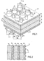
- the filter 3 FIG. 1 extends in a symmetry with respect to its median plane 12: it comprises, on either side of this plane, a substrate 13 covered with a thin layer 14 in part of the thickness of which have been formed by etching pads 15, 16 forming a network resonant.
- This network comprises on the one hand a plurality of first pads 15, of cylindrical shape along axes parallel to the normal 8 to the face upper outer 9 and the lower outer face 17 of the component 3, and circular cross section (or contour); the network comprises on the other hand a plurality of second pads 16 of shape also cylindrical and parallel to normal 8 to plane 12.
- the studs 15 are of identical shape and size and are regularly spaced in two orthogonal directions perpendicular to the normal 8 to form a first square mesh.
- the studs 16 are also of identical shape and size and are spaced according to said perpendicular orthogonal directions to normal 8 to form a second square mesh, which is nested with the first square mesh.
- the pads 15, 16 thus form a two-sided bipedal network. dimensions that extends to the surface of the layer 14.
- the longitudinal 21 and transverse 18 steps of the two meshes are identical and smaller than the filtering wavelength, but the diameter 19, 20 and / or the respective height of the studs 15, 16 is (are different).
- Component 3 thus comprises two identical networks respectively provided on its outer surface 9 and on its face lower end 17, so as to form a band-pass filter in transmission; the central frequency (wavelength) of this filter is calculated by the usual methods in the field, according to the optical and geometric characteristics of the pads 15, 16 and the layer 14 on which these pads are formed; this layer constitutes a waveguide with its own frequencies (temporal and spatial) of resonance.
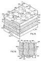
- the bandpass filter 4 in reflection can be constituted by several structures resonant stacked along axis 8 (normal incidence) which is perpendicular to the faces of the layers: this filter comprises a substrate 13 covered with a thin layer 14 in part of the thickness of which is etched a first resonant network; a layer 22 forming a substrate (or "spacer" spacer) covers the layer 14 and is itself coated with a thin layer 23 having a second network resonant; a layer 24 similar to the layer 22 covers the layer 23 and is coated with a thin layer 25 having a third resonant network.
- an example of a component not forming part of the invention can be obtained by gluing or adhesion of two portions obtained by cutting along the lines 26, 27 of the blank illustrated in Figure 4; this blank comprises a substrate 28 covered with two thin layers 29 and 30; in part of the layer 30 (or in a layer covering it) were formed a plurality of patterns 31, 32 pyramids of square section, of identical shape and size; the patterns 31 form a first network extending in the first portion 33 of the draft, while the reasons 32 form a second network (of characteristics identical to the first) in a second portion 34 of the component blank.
- the two portions 33, 34 are separable by a section according to the plane defined by the lines 26, 27, and are then secured by the face 35 of their substrate 28 respectively.
- the lateral faces (or flanks) 36, 37 of the pad 38 of a grating formed on the surface 9 of the thin layer 40 are inclined, relative to a normal 8a at the surface 9, of an angle 41.
- the filters can be aligned along the axis 50, their respective planes 12a being arranged parallel to each other others and regularly spaced a step apart 51.
- the transmitter filters 3 extend in two parallel planes 12b, 12c and are regularly spaced by one step 52.
- the network 60 comprises a plurality of square meshes 61 of width 62 which are arranged side by side and extend in two orthogonal directions contained in the plane of the figure.
- the studs 63 1 are regularly spaced a step whose value is equal to the width 62 of the mesh; the studs 63 2 are also spaced apart from each other with the same pitch, as well as the studs 65 between them on the one hand and as the studs 67 between them on the other hand.
- each mesh The four studs of each mesh are arranged so that that their respective centers are arranged at the top of a square whose the side 70 corresponds to half of the side 62 of the mesh 61.
- the engraved studs 63, 65, 67 can be replaced by patterns doped form (contour) and spacing identical or similar.
- the demultiplexer 1001, 1002 has eight filters 1003 (respectively four filters 1004) bandpass centered on eight (or four) wavelengths different corresponding to the eight (respectively four) channels to to separate.
- the demultiplexer has a coupling interface 1005 optical fiber with a 1006 optical fiber carrying radiation to to divide ; the incident beam 1007 delivered by the fiber 1006 forms with the normal 1008 to the face 1009 of the filter an angle of incidence 1010, whose value is the lowest possible in order to limit disturbances likely to result.
- FIG. 14 has four collimators 1011 respectively associated with the four filters 1004, which used to direct to an optical fiber 1110 output part of the incident beam 1007 which corresponds to the wavelength associated with the corresponding channel, and that was reflected by the 1004 filter corresponding.
- each demultiplexer 1001, 1002 can have an integrated input collimator to limit the opening of the incident beam 1007 from the fiber.
- the filters 1003 and 1004 have a plate structure as illustrated respectively Figures 10 and 11.
- Each output collimator 1011 can be constituted by the doped end of the corresponding output fiber 1110; the end input fiber 1006 can also be doped to form a collimator 1005.
- Each demultiplexer 1001, 1002 includes a waveguide 1100 which is formed in a layer deposited on a substrate, and which is extended by other guides 1101; this layer is provided with grooves substantially transverse to the longitudinal axis of the guides 1100, 1101, each groove receiving a transversely arranged filter to waveguide portions 1100, 1101; so the spectral component of the beam 1007 propagating in the guides 1100, 1101, which corresponds to the wavelength on which the filter is centered, crosses this one in the case of Figure 12 or on the contrary is reflected by the filter in the case of Figure 14.
- This filtered component is transmitted by a waveguide 1102 output to the output fiber 1110; in the case of Figure 14, the end of the guide 1102 is doped to form the collimator 1011 of exit.
- the filter 1003 FIG. 10 extends in a symmetry with respect to its median plane 1012: it includes, on both sides of this plane, a substrate 1013 covered with a thin layer 1014 in the thickness of which were formed by ion implantation, doped patterns 1015, 1016 forming a resonant network.
- This network comprises on the one hand a plurality of first patterns 1015, cylindrical in axes parallel to normal 1008 at the upper outer face 1009 and the lower outer face 1017 of the component 1003, and circular cross section (and / or contour) circular; the network comprises on the other hand a plurality of second patterns 1016 of shape also cylindrical and parallel to the normal plane 1008 1012.
- the patterns 1015 are of identical shape and size and are regularly spaced in two orthogonal directions perpendicular to the normal 1008 to form a first mesh square.
- Patterns 1016 are also shaped and dimensioned identical and are spaced according to said orthogonal directions perpendicular to the normal 1008 to form a second mesh square, which is nested with the first square mesh.
- the patterns 1015, 1016 thus form a bi Southernodic network to two dimensions that extends inside the layer 1014.
- the longitudinal 1021 and transverse 1018 steps of two meshes are identical and smaller than the wavelength corresponding to the central frequency of filtering, but the diameter 1019, 1020 and / or the respective height of the patterns 1015, 1016 is (are) different).
- the component 1003 thus comprises two identical networks respectively provided on its outer surface 1009 and on its lower face 1017, so as to form a band-pass filter in transmission; the central frequency (wavelength) of this filter is calculated by the usual methods in the field, according to the optical and geometric characteristics of patterns 1015, 1016 and the layer 1014 in which these patterns are formed; this layer constitutes a waveguide with its own frequencies (temporal and spatial) of resonance.
- the reflection bandpass filter 1004 may consist of several resonant structures stacked along axis 1008 (normal incidence) which is perpendicular to the faces of the layers: this filter comprises a substrate 1013 covered with a thin layer 1014 in the thickness of which is implanted a first resonant network; a layer 1022 forming a substrate (spacer spacer) covers the layer 1014 and is itself coated with a thin layer 1023 having a second resonant network; a layer 1024 similar to the layer 1022 covers the layer 1023 and is coated with a thin layer 1025 having a third resonant network.
- the lateral faces (or flanks) 1036, 1037 of the pattern 1038 of a network formed under the surface 1009 of the 1040 thin layer are inclined, compared to a normal 1008a to the surface 1009, an angle 1041.
- the filters can be aligned along the axis 1050, their respective planes 1012a being arranged parallel to one another to others and regularly spaced a step 1051.
- Transmitters 1003 extend in two parallel planes 1012b, 1012c and are regularly spaced a step 1052 apart.
- the filter 2003 figure 15 extends in a symmetry with respect to its 2012 median plan: it includes, on both sides of this plan, a 2013 substrate covered with a thin layer 2014 in the thickness of which were formed by ion implantation, doped patterns 2015, 2016 forming a resonant network.
- This network comprises on the one hand a plurality of first patterns 2015, cylindrical in parallel to normal 2008 to the upper outer face 2009 and the lower outer face 2017 of the component 2003, and circular cross section (or contour); the network comprises on the other hand a plurality of second patterns 2016 of also cylindrical shape and parallel to the 2008 normal to the 2012 plan and thin layers.
- the 2015 motifs are of identical shape and size and are regularly spaced in two orthogonal directions perpendicular to the normal 2008 to form a first mesh square.
- 2016 motifs are also shaped and dimensioned identical and are spaced according to said orthogonal directions perpendicular to the normal 2008 to form a second mesh square, which is nested with the first square mesh.
- the 2015, 2016 motifs thus form a bigesrodique network to two dimensions that extends inside the 2014 layer.
- the longitudinal 2021 and transverse 2018 two meshes are identical, but the diameter 2019, 2020 and / or the respective height of the reasons 2015, 2016 is (are) different (s).
- the 2003 component thus includes two identical networks respectively provided on its external 2009 external face and on its external underside 2017, so as to form a bandpass filter in transmission; the central frequency (wavelength) of this filter is calculated by the usual methods in the field, according to the optical and geometric characteristics of the motifs 2015, 2016 and the layer 2014 in which these patterns are formed; this layer constitutes a waveguide with its own frequencies (temporal and spatial) of resonance.
- Each of the two thin layers 2014 in which are formed patterns 2015, 2016, is made of a partially material crystal with piezoelectric, photoelectric and / or refractive photo; each layer 2014 is in electrical contact by two opposite parts of his wafer with two electrodes 2140 respectively connected to the two terminals of a generator 2141 of electrical control signals.
- This construction makes it possible to apply an electric field between said two opposing portions of the slice of each layer 2014; he results in a modification of the geometrical characteristics and / or optics of each layer 2014, and therefore a variation of resonant frequency of the resonant structure formed in the active layers 2014.
- the filter 2004 bandpass in reflection is constituted by several structures resonant stacked along the axis 2008 (normal incidence) which is perpendicular to the faces of the layers: this filter comprises a substrate 2013, as well as a thin layer 2014 in part of the thickness of which is etched a first resonant network.
- the 2014 layer extends between two active thin layers 2200 and 2201 which are respectively connected by two conductive elements (forming electrodes) 2300 and 2301 at the terminals of a power source electric; when this source delivers a voltage between its terminals, this voltage is applied to layers 2200 and 2201 and causes a modification of the characteristics of the layer 2014 that they enclose; this results in a modification of the characteristics of the 2004 filter.
- a second stack comprises a layer 2022 forming a substrate (spacer spacer) and covering the layer 2201, and a thin layer 2023 having a second network resonant and sandwiched between two layers 2202 and 2203;
- a third stack has a layer 2024 similar to the layer 2022 covering the layer 2203, and a thin layer 2025 having a third etched resonant grating, which layer 2025 extends between two active thin layers 2204 and 2205.
- the lateral faces (or flanks) 2036, 2037 of the pattern 2038 of a network formed under the 2009 surface of the thin layer 2040 are inclined, compared to a normal 2008a to the 2009 surface, from an angle 2041; the active thin layer 2040 is equipped on two portions of its slice of two electrodes allowing the application of a transverse electric field in the layer 2040.
- the nine filters 2004 reflective ones extend in five parallel planes and are regularly spaced so that their optical centers are arranged at the vertices of a square mesh.
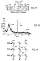
- the diffraction spectrum 2400 has a peak 2401 revealing the existence of a crystalline structure in the active thin layer; the rest of the spectrum, including the bump 2402, being significant of an amorphous structure.
Claims (27)
- Optisches Bauteil zum Filtern einer bestimmten Wellenlänge (3, 4, 1003, 1004), umfassend mindestens eine dünne Schicht (14, 23, 25, 29, 30, 40), die auf einem Substrat (13, 28) abgeschieden ist, sowie eine resonierende Struktur oder ein resonierendes Gitter, die bzw. das eine Vielzahl von Motiven (15, 16, 31, 32, 38, 63, 65, 67) umfasst, die in der dünnen Schicht gebildet sind, dadurch gekennzeichnet, dass die resonierende Struktur oder das resonierende Gitter (60) umfasst:wobei sich die zweite Abmessung oder die zweite Ionenkonfiguration von der ersten Abmessung oder Ionenkonfiguration unterscheidet,eine Vielzahl von ersten Motiven (15) mit einer ersten Abmessung oder einer ersten Ionenkonfiguration, die allen ersten Motiven gemeinsam ist, wobei die ersten Motive in zwei unterschiedlichen Richtungen, die parallel zur dünnen Schicht sind, und mit einem Schritt (62), der kleiner als die gefilterte Wellenlänge ist, regelmäßig voneinander beabstandet sind;eine Vielzahl von zweiten Motiven (16) mit einer zweiten Abmessung oder einer zweiten Ionenkonfiguration, die allen zweiten Motiven gemeinsam ist, wobei die zweiten Motive in den zwei Richtungen, die parallel zur dünnen Schicht sind, und mit einem Schritt (62), der identisch mit dem Schritt der ersten Abstandsmotive ist, regelmäßig voneinander beabstandet sind,
so dass ein Reflexions-Bandfilter für einen Einfall nahe der Normalen zur genannten dünnen Schicht gebildet wird. - Bauteil nach Anspruch 1, in dem die Motive in die dünne Schicht geätzt sind.
- Bauteil nach einem der Ansprüche 1 oder 2, das umfasst:ein erstes mehrperiodisches resonierendes Gitter (15, 16, 31, 32, 38), das in mindestens eine erste dünne Schicht geätzt oder implantiert ist,ein zweites mehrperiodisches resonierendes Gitter, das in mindestens eine zweite dünne Schicht geätzt oder implantiert ist,mindestens eine dritte dünne Schicht, die einen ersten Kopplungs- und Entkopplungsbereich bildet, der dem ersten Gitter zugeordnet ist.
- Bauteil nach Anspruch 3, das darüber hinaus umfasst:mindestens eine vierte dünne Schicht, die einen zweiten Kopplungs- und Entkopplungsbereich bildet, der dem zweiten Gitter zugeordnet ist,mindestens eine dicke Schicht, die das Substrat bildet.
- Bauteil nach einem der Ansprüche 1 bis 4, das zwei resonierende Strukturen oder Gitter umfasst, die symmetrisch in Bezug auf eine Mittelebene (12, 12b, 12c) des Bauteils angeordnet sind, so dass ein Transmissions-Bandfilter (3) gebildet wird.
- Bauteil nach einem der Ansprüche 1 bis 5, in dem die Motive einen annähernd kreisförmigen oder quadratischen Querschnitt haben.
- Bauteil nach einem der Ansprüche 1 bis 6, in dem die Motive des Gitters in einer äußeren dünnen Schicht gebildet sind, deren Index kleiner ist als jener der Schicht, die die äußere dünne Schicht trägt.
- Bauteil nach einem der Ansprüche 1 bis 7, dessen resonierende Struktur ein Gitter von Stufen (38) umfasst, deren Seitenflächen (36, 37) geneigt sind.
- Bauteil nach einem der Ansprüche 1 bis 8, das mindestens drei resonierende Gitter umfasst, die in drei übereinandergelagerten dünnen Schichten (14, 23, 25) vorgesehen sind.
- Bauteil nach einem der Ansprüche 1 bis 9, das weniger als zehn dünne Schichten umfasst, insbesondere eine, zwei oder drei dünne Schichten, die jeder resonierenden Struktur zugeordnet ist (sind) und deren Durchlassbereich auf eine Wellenlänge in der Nähe von 1,5 Mikron zentriert ist.
- Bauteil nach einem der Ansprüche 1 oder 3 bis 10, in dem die Motive im Wesentlichen aus gedopten Bereichen der dünnen Schicht gebildet werden.
- Bauteil nach Anspruch 11, in dem die transversalen Indexprofile (36, 37) der Motive geneigt sind.
- Optischer Multiplexer oder Demultiplexer (1, 2) mit Wellenlängenteilung, der eine Vielzahl von Bauteilen umfasst, insbesondere von 8 oder 16 bis 256 Bauteile (3, 4) nach einem der Ansprüche 1 bis 12.
- Multiplexer oder Demultiplexer nach Anspruch 13, in dem die Bauteile (3, 4) mechanisch miteinander verbunden sind, jeweils unterschiedliche zentrale Wellenlängen aufweisen und sich im Wesentlichen parallel zueinander erstrecken, und der darüber hinaus einen jedem Bauteil (3, 4) zugeordneten Kollimator (11) und gegebenenfalls einen Kollimator (5) oder Wellenleiter umfasst, der zur optischen Kopplung des Multiplexers oder Demultplexers mit dem Ansatz einer Lichtleitfaser (6) geeignet ist.
- Multiplexer oder Demultiplexer nach Anspruch 13 oder 14, in dem die Bauteile, die Reflexionsfilter bilden, so angeordnet sind, dass sie nach einer allen Bauteilen gemeinsamen Achse (50) ausgerichtet sind.
- Multiplexer oder Demultiplexer nach Anspruch 13 oder 14, in dem die Bauteile, die Transmissionsfilter bilden, in mindestens zwei Ebenen (12b, 12c) angeordnet sind, die im Wesentlichen parallel zueinander sind.
- Verfahren zur Herstellung eines Bauteils gemäß einem der Ansprüche 1 bis 12, in dem eine bis zehn dünne Schichten auf einem Substrat abgeschieden werden und in dem ein Gitter durch einen Elektronenstrahl oder durch Lithographie auf eine dünne Schicht geätzt wird.
- Verfahren zur Herstellung eines Bauteils gemäß einem der Ansprüche 1 bis 12, in dem eine bis zehn dünne Schichten auf einem Substrat abgeschieden werden und in dem ein Gitter durch einen Ionenstrahl, der von einem Ionenimplantator geliefert wird, auf einer dünnen Schicht implantiert wird.
- Verfahren nach Anspruch 17 oder 18, bei dem mindestens zwei Bauteile, deren Gitter identisch sind, aufeinandergestapelt und miteinander verbunden werden.
- Verfahren nach einem der Ansprüche 17 bis 19, bei dem die zentrale Wellenlänge des Filters durch Abscheiden einer dünnen Schicht auf dem Gitter oder durch Ätzen eingestellt wird.
- Bauteil nach einem der Ansprüche 1 bis 12, in dem mindestens eine dünne Schicht aus einem nicht amorphen Material gebildet wird, um ein aktives Bandfilter zu bilden.
- Bauteil nach Anspruch 21, in dem das Material, das die aktive dünne Schicht bildet, durchlässig für die Arbeitswellenlängen insbesondere im Infrarotbereich ist.
- Bauteil nach einem der Ansprüche 21 oder 22, in dem das Material, das die aktive dünne Schicht bildet, teilweise kristallin und mit piezoelektrischen und/oder photoelektrischen Eigenschaften versehen ist und aus der Gruppe, bestehend aus LiNbO3, BaTiO3, ZnO, Ta2O5 und modifiziertem ITO, gewählt wird.
- Bauteil nach einem der Ansprüche 21 bis 23, in dem das resonierende Gitter in der aktiven Schicht (2014) gebildet ist, die in elektrischem Kontakt mit zwei Elektroden (2140) ist.
- Bauteil nach einem der Ansprüche 21 bis 23, in dem das resonierende Gitter zwischen zwei aktiven Schichten (2200, 2201) eingefügt ist, die jeweils in Kontakt mit einer Elektrode (2300, 2301) sind.
- Optische Vorrichtung mit Wellenlängenteilung, insbesondere optischer Multiplexer oder Demultiplexer (1, 2), der eine Vielzahl von Bauteilen umfasst, insbesondere von 8 oder 16 bis 256 Bauteile (2003, 2004) nach einem der Ansprüche 21 bis 25, in dem die Bauteile (2003, 2004) mechanisch miteinander verbunden sind, vorzugsweise jeweils unterschiedliche zentrale Wellenlängen aufweisen und sich im Wesentlichen parallel zueinander erstrecken, und der darüber hinaus ein jedem Bauteil (2003, 2004) zugeordnetes Kollimationsmittel (11) und gegebenenfalls ein Kollimationsmittel (5) oder einen Wellenleiter umfasst, das bzw. der zur optischen Kopplung der Vorrichtung mit dem Ansatz einer Lichtleitfaser (6) geeignet ist.
- Verfahren zur Herstellung eines Bauteils gemäß einem der Ansprüche 21 bis 25, bei dem die aktive dünne Schicht gebildet wird, indem ein Material bei hoher Temperatur aufgetragen wird, insbesondere bei einer Temperatur in einem Bereich von 200°C bis 900°C, wenn Ta2O5 verwendet wird, und/oder indem ein Ionen- oder Elektronenstrahl verwendet wird, dessen Energie ausreichend ist, um ein Ablösen von kristallinen Strukturen hervorzurufen.
Applications Claiming Priority (7)
| Application Number | Priority Date | Filing Date | Title |
|---|---|---|---|
| FR0013122A FR2815417B1 (fr) | 2000-10-13 | 2000-10-13 | Filtre optique, son procede de fabrication et son utilisation pour un systeme multiplex |
| FR0013122 | 2000-10-13 | ||
| FR0013869 | 2000-10-27 | ||
| FR0013870A FR2816063B1 (fr) | 2000-10-27 | 2000-10-27 | Filtre optique actif, son procede de fabrication et son utilisation pour un systeme mulitplex |
| FR0013869A FR2816062B1 (fr) | 2000-10-27 | 2000-10-27 | Filtre optique, son procede de fabrication par dopage ionique et son utilisation pour un systeme multiplex |
| FR0013870 | 2000-10-27 | ||
| PCT/FR2001/003159 WO2002031551A1 (fr) | 2000-10-13 | 2001-10-12 | Filtres optiques, leur procede de fabrication et leur utilisation pour un systeme multiplexe |
Publications (2)
| Publication Number | Publication Date |
|---|---|
| EP1417521A1 EP1417521A1 (de) | 2004-05-12 |
| EP1417521B1 true EP1417521B1 (de) | 2005-12-14 |
Family
ID=27248710
Family Applications (1)
| Application Number | Title | Priority Date | Filing Date |
|---|---|---|---|
| EP01976412A Expired - Lifetime EP1417521B1 (de) | 2000-10-13 | 2001-10-12 | Optische filter, ihre herstellungsverfahren und ihre anwendung für ein multiplexsystem |
Country Status (4)
| Country | Link |
|---|---|
| EP (1) | EP1417521B1 (de) |
| AU (1) | AU2001295694A1 (de) |
| DE (1) | DE60115966T2 (de) |
| WO (1) | WO2002031551A1 (de) |
Families Citing this family (6)
| Publication number | Priority date | Publication date | Assignee | Title |
|---|---|---|---|---|
| GB0201969D0 (en) | 2002-01-29 | 2002-03-13 | Qinetiq Ltd | Integrated optics devices |
| GB0306008D0 (en) | 2003-03-15 | 2003-04-23 | Qinetiq Ltd | Optical device |
| GB0306634D0 (en) | 2003-03-22 | 2003-04-30 | Qinetiq Ltd | Optical wavelength division multiplexer/demultiplexer device |
| US20060215954A1 (en) | 2004-03-22 | 2006-09-28 | Jenkins Richard M | Optical routing device comprising hollow waveguides and mems reflective elements |
| FR2856804B1 (fr) * | 2003-06-26 | 2005-11-11 | Cilas Marseille | Filtres optiques a reseau resonnant |
| WO2018222839A1 (en) * | 2017-06-01 | 2018-12-06 | Radiabeam Technologies, Llc | Split structure particle accelerators |
Family Cites Families (17)
| Publication number | Priority date | Publication date | Assignee | Title |
|---|---|---|---|---|
| US3868589A (en) * | 1972-10-10 | 1975-02-25 | Univ California | Thin film devices and lasers |
| US3970959A (en) * | 1973-04-30 | 1976-07-20 | The Regents Of The University Of California | Two dimensional distributed feedback devices and lasers |
| US4496216A (en) * | 1982-12-30 | 1985-01-29 | Polaroid Corporation | Method and apparatus for exposing photosensitive material |
| JPS6476005A (en) * | 1987-09-17 | 1989-03-22 | Ricoh Kk | Wavelength multiple optical demultiplexer |
| US5157537A (en) * | 1991-02-01 | 1992-10-20 | Yeda Research And Development Co., Ltd. | Distributed resonant cavity light beam modulator |
| SE468188B (sv) * | 1991-04-08 | 1992-11-16 | Stiftelsen Inst Foer Mikroelek | Metod foer inkoppling av straalning i en infraroeddetektor, jaemte anordning |
| US5245596A (en) * | 1991-06-26 | 1993-09-14 | Eastman Kodak Company | Optical head having a grating with a doubly periodic structure |
| US5216680A (en) * | 1991-07-11 | 1993-06-01 | Board Of Regents, The University Of Texas System | Optical guided-mode resonance filter |
| DE4228853C2 (de) * | 1991-09-18 | 1993-10-21 | Schott Glaswerke | Optischer Wellenleiter mit einem planaren oder nur geringfügig gewölbten Substrat und Verfahren zu dessen Herstellung sowie Verwendung eines solchen |
| US5434708A (en) * | 1992-09-08 | 1995-07-18 | Eastman Kodak Company | Optical reproducing apparatus ultilizing a polarization beam splitter |
| IL118209A0 (en) * | 1996-05-09 | 1998-02-08 | Yeda Res & Dev | Active electro-optical wavelength-selective mirrors and active electro-optic wavelength-selective filters |
| US5892230A (en) * | 1997-05-29 | 1999-04-06 | Massachusetts Institute Of Technology | Scintillating fiducial patterns |
| US6035089A (en) * | 1997-06-11 | 2000-03-07 | Lockheed Martin Energy Research Corporation | Integrated narrowband optical filter based on embedded subwavelength resonant grating structures |
| FR2775355B1 (fr) * | 1998-02-26 | 2000-03-31 | Alsthom Cge Alcatel | Reflecteur optique en semi-conducteur et procede de fabrication |
| JP4172057B2 (ja) * | 1998-04-28 | 2008-10-29 | 松下電器産業株式会社 | 偏光性回折格子の作成方法 |
| JP3627093B2 (ja) * | 1999-03-24 | 2005-03-09 | 大阪府 | 共振モード格子フィルター |
| KR100390875B1 (ko) * | 1999-10-27 | 2003-07-10 | (주)해빛정보 | 위상 회절 격자형 광 저대역 통과필터 |
-
2001
- 2001-10-12 EP EP01976412A patent/EP1417521B1/de not_active Expired - Lifetime
- 2001-10-12 WO PCT/FR2001/003159 patent/WO2002031551A1/fr active IP Right Grant
- 2001-10-12 DE DE60115966T patent/DE60115966T2/de not_active Expired - Fee Related
- 2001-10-12 AU AU2001295694A patent/AU2001295694A1/en not_active Abandoned
Also Published As
| Publication number | Publication date |
|---|---|
| WO2002031551A1 (fr) | 2002-04-18 |
| DE60115966D1 (de) | 2006-01-19 |
| EP1417521A1 (de) | 2004-05-12 |
| AU2001295694A1 (en) | 2002-04-22 |
| DE60115966T2 (de) | 2006-07-06 |
Similar Documents
| Publication | Publication Date | Title |
|---|---|---|
| EP0196948B1 (de) | Umkehrbare Demultiplexeinrichtung von einer Mehrzahl von Lichtsignalen in integrierter Optik | |
| EP0005093B1 (de) | Optische integrierte Demultiplexieranordnung und Verfahren zu seiner Herstellung | |
| EP3610309B1 (de) | Photonischer chip mit integrierter kollimationsstruktur | |
| FR2694816A1 (fr) | Filtre optique accordable. | |
| EP3521879A1 (de) | Photonischer chip mit integrierter kollimationsstruktur | |
| EP1474711B1 (de) | Abstimmbares optisches filter | |
| EP0564347A1 (de) | Wellenlängenmultiplexer, insbesondere für optisches integriertes System | |
| EP2141520A1 (de) | Kupplungsvorrichtung mit kompensierter Doppelbrechung | |
| FR2775355A1 (fr) | Reflecteur optique en semi-conducteur et procede de fabrication | |
| EP0703473B1 (de) | Integriert-optoelektronische Vorrichtung zur Aufspaltung und Erkennung von verschiedenen Wellenlängen | |
| EP1417521B1 (de) | Optische filter, ihre herstellungsverfahren und ihre anwendung für ein multiplexsystem | |
| FR2477287A2 (fr) | Repartiteur optique multiple de la lumiere, procede de realisation d'un filtre interferentiel pour un tel repartiteur et mise en oeuvre de ce repartiteur | |
| FR2655430A1 (fr) | Coupeur optique et systeme informatique a processeurs repartis. | |
| FR2743234A1 (fr) | Demultiplexeur de longueurs d'onde | |
| EP3491438B1 (de) | Multispektraler optischer koppler mit niedrigen empfangsverlusten | |
| EP0881527B1 (de) | Räumliches optisches Schaltsystem mit akustooptischem Mehrkanal-Ablenker | |
| EP1058138A1 (de) | Multiplexer/Demultiplexer mit drei Wellenleitern | |
| FR2816063A1 (fr) | Filtre optique actif, son procede de fabrication et son utilisation pour un systeme mulitplex | |
| CA3025328A1 (fr) | Element de blindage electromagnetique optiquement transparent et a plusieurs zones | |
| EP0370577B1 (de) | Integrierte Halbleiter-Vorrichtung mit einem optoelektronischen Schaltelement | |
| FR3060772A1 (fr) | Circuit photonique integre optimise | |
| FR2816062A1 (fr) | Filtre optique, son procede de fabrication par dopage ionique et son utilisation pour un systeme multiplex | |
| EP1291707A1 (de) | Optischer sättigbarer Absorber und dessen Verwendung zum Regenerieren eines Wellenmultiplexsignales | |
| FR2815417A1 (fr) | Filtre optique, son procede de fabrication et son utilisation pour un systeme multiplex | |
| EP1546770B1 (de) | Optische filterkomponente mit flacher oberseite |
Legal Events
| Date | Code | Title | Description |
|---|---|---|---|
| PUAI | Public reference made under article 153(3) epc to a published international application that has entered the european phase |
Free format text: ORIGINAL CODE: 0009012 |
|
| 17P | Request for examination filed |
Effective date: 20030805 |
|
| AK | Designated contracting states |
Kind code of ref document: A1 Designated state(s): AT BE CH CY DE DK ES FI FR GB GR IE IT LI LU MC NL PT SE TR |
|
| RBV | Designated contracting states (corrected) |
Designated state(s): CH DE GB LI |
|
| GRAP | Despatch of communication of intention to grant a patent |
Free format text: ORIGINAL CODE: EPIDOSNIGR1 |
|
| GRAS | Grant fee paid |
Free format text: ORIGINAL CODE: EPIDOSNIGR3 |
|
| GRAA | (expected) grant |
Free format text: ORIGINAL CODE: 0009210 |
|
| AK | Designated contracting states |
Kind code of ref document: B1 Designated state(s): CH DE GB LI |
|
| REG | Reference to a national code |
Ref country code: GB Ref legal event code: FG4D Free format text: NOT ENGLISH |
|
| REG | Reference to a national code |
Ref country code: CH Ref legal event code: EP |
|
| GBT | Gb: translation of ep patent filed (gb section 77(6)(a)/1977) |
Effective date: 20051214 |
|
| REF | Corresponds to: |
Ref document number: 60115966 Country of ref document: DE Date of ref document: 20060119 Kind code of ref document: P |
|
| PLBE | No opposition filed within time limit |
Free format text: ORIGINAL CODE: 0009261 |
|
| STAA | Information on the status of an ep patent application or granted ep patent |
Free format text: STATUS: NO OPPOSITION FILED WITHIN TIME LIMIT |
|
| 26N | No opposition filed |
Effective date: 20060915 |
|
| PGFP | Annual fee paid to national office [announced via postgrant information from national office to epo] |
Ref country code: DE Payment date: 20081107 Year of fee payment: 8 |
|
| PGFP | Annual fee paid to national office [announced via postgrant information from national office to epo] |
Ref country code: CH Payment date: 20090923 Year of fee payment: 9 |
|
| PGFP | Annual fee paid to national office [announced via postgrant information from national office to epo] |
Ref country code: GB Payment date: 20091007 Year of fee payment: 9 |
|
| PG25 | Lapsed in a contracting state [announced via postgrant information from national office to epo] |
Ref country code: DE Free format text: LAPSE BECAUSE OF NON-PAYMENT OF DUE FEES Effective date: 20100501 |
|
| REG | Reference to a national code |
Ref country code: CH Ref legal event code: PL |
|
| GBPC | Gb: european patent ceased through non-payment of renewal fee |
Effective date: 20101012 |
|
| PG25 | Lapsed in a contracting state [announced via postgrant information from national office to epo] |
Ref country code: LI Free format text: LAPSE BECAUSE OF NON-PAYMENT OF DUE FEES Effective date: 20101031 Ref country code: CH Free format text: LAPSE BECAUSE OF NON-PAYMENT OF DUE FEES Effective date: 20101031 |
|
| PG25 | Lapsed in a contracting state [announced via postgrant information from national office to epo] |
Ref country code: GB Free format text: LAPSE BECAUSE OF NON-PAYMENT OF DUE FEES Effective date: 20101012 |