EP1416546A1 - Method of making a laminated ceramic with a non-planar structure - Google Patents
Method of making a laminated ceramic with a non-planar structure Download PDFInfo
- Publication number
- EP1416546A1 EP1416546A1 EP02023464A EP02023464A EP1416546A1 EP 1416546 A1 EP1416546 A1 EP 1416546A1 EP 02023464 A EP02023464 A EP 02023464A EP 02023464 A EP02023464 A EP 02023464A EP 1416546 A1 EP1416546 A1 EP 1416546A1
- Authority
- EP
- European Patent Office
- Prior art keywords
- laminate
- laminating step
- green
- ceramic
- temperature
- Prior art date
- Legal status (The legal status is an assumption and is not a legal conclusion. Google has not performed a legal analysis and makes no representation as to the accuracy of the status listed.)
- Withdrawn
Links
Images

Classifications
-
- B—PERFORMING OPERATIONS; TRANSPORTING
- B32—LAYERED PRODUCTS
- B32B—LAYERED PRODUCTS, i.e. PRODUCTS BUILT-UP OF STRATA OF FLAT OR NON-FLAT, e.g. CELLULAR OR HONEYCOMB, FORM
- B32B18/00—Layered products essentially comprising ceramics, e.g. refractory products
-
- C—CHEMISTRY; METALLURGY
- C04—CEMENTS; CONCRETE; ARTIFICIAL STONE; CERAMICS; REFRACTORIES
- C04B—LIME, MAGNESIA; SLAG; CEMENTS; COMPOSITIONS THEREOF, e.g. MORTARS, CONCRETE OR LIKE BUILDING MATERIALS; ARTIFICIAL STONE; CERAMICS; REFRACTORIES; TREATMENT OF NATURAL STONE
- C04B35/00—Shaped ceramic products characterised by their composition; Ceramics compositions; Processing powders of inorganic compounds preparatory to the manufacturing of ceramic products
- C04B35/01—Shaped ceramic products characterised by their composition; Ceramics compositions; Processing powders of inorganic compounds preparatory to the manufacturing of ceramic products based on oxide ceramics
- C04B35/48—Shaped ceramic products characterised by their composition; Ceramics compositions; Processing powders of inorganic compounds preparatory to the manufacturing of ceramic products based on oxide ceramics based on zirconium or hafnium oxides, zirconates, zircon or hafnates
- C04B35/49—Shaped ceramic products characterised by their composition; Ceramics compositions; Processing powders of inorganic compounds preparatory to the manufacturing of ceramic products based on oxide ceramics based on zirconium or hafnium oxides, zirconates, zircon or hafnates containing also titanium oxides or titanates
- C04B35/491—Shaped ceramic products characterised by their composition; Ceramics compositions; Processing powders of inorganic compounds preparatory to the manufacturing of ceramic products based on oxide ceramics based on zirconium or hafnium oxides, zirconates, zircon or hafnates containing also titanium oxides or titanates based on lead zirconates and lead titanates, e.g. PZT
-
- C—CHEMISTRY; METALLURGY
- C04—CEMENTS; CONCRETE; ARTIFICIAL STONE; CERAMICS; REFRACTORIES
- C04B—LIME, MAGNESIA; SLAG; CEMENTS; COMPOSITIONS THEREOF, e.g. MORTARS, CONCRETE OR LIKE BUILDING MATERIALS; ARTIFICIAL STONE; CERAMICS; REFRACTORIES; TREATMENT OF NATURAL STONE
- C04B35/00—Shaped ceramic products characterised by their composition; Ceramics compositions; Processing powders of inorganic compounds preparatory to the manufacturing of ceramic products
- C04B35/622—Forming processes; Processing powders of inorganic compounds preparatory to the manufacturing of ceramic products
- C04B35/626—Preparing or treating the powders individually or as batches ; preparing or treating macroscopic reinforcing agents for ceramic products, e.g. fibres; mechanical aspects section B
- C04B35/63—Preparing or treating the powders individually or as batches ; preparing or treating macroscopic reinforcing agents for ceramic products, e.g. fibres; mechanical aspects section B using additives specially adapted for forming the products, e.g.. binder binders
- C04B35/632—Organic additives
- C04B35/634—Polymers
- C04B35/63404—Polymers obtained by reactions only involving carbon-to-carbon unsaturated bonds
- C04B35/63408—Polyalkenes
-
- C—CHEMISTRY; METALLURGY
- C04—CEMENTS; CONCRETE; ARTIFICIAL STONE; CERAMICS; REFRACTORIES
- C04B—LIME, MAGNESIA; SLAG; CEMENTS; COMPOSITIONS THEREOF, e.g. MORTARS, CONCRETE OR LIKE BUILDING MATERIALS; ARTIFICIAL STONE; CERAMICS; REFRACTORIES; TREATMENT OF NATURAL STONE
- C04B35/00—Shaped ceramic products characterised by their composition; Ceramics compositions; Processing powders of inorganic compounds preparatory to the manufacturing of ceramic products
- C04B35/622—Forming processes; Processing powders of inorganic compounds preparatory to the manufacturing of ceramic products
- C04B35/626—Preparing or treating the powders individually or as batches ; preparing or treating macroscopic reinforcing agents for ceramic products, e.g. fibres; mechanical aspects section B
- C04B35/63—Preparing or treating the powders individually or as batches ; preparing or treating macroscopic reinforcing agents for ceramic products, e.g. fibres; mechanical aspects section B using additives specially adapted for forming the products, e.g.. binder binders
- C04B35/632—Organic additives
- C04B35/634—Polymers
- C04B35/63404—Polymers obtained by reactions only involving carbon-to-carbon unsaturated bonds
- C04B35/63416—Polyvinylalcohols [PVA]; Polyvinylacetates
-
- C—CHEMISTRY; METALLURGY
- C04—CEMENTS; CONCRETE; ARTIFICIAL STONE; CERAMICS; REFRACTORIES
- C04B—LIME, MAGNESIA; SLAG; CEMENTS; COMPOSITIONS THEREOF, e.g. MORTARS, CONCRETE OR LIKE BUILDING MATERIALS; ARTIFICIAL STONE; CERAMICS; REFRACTORIES; TREATMENT OF NATURAL STONE
- C04B35/00—Shaped ceramic products characterised by their composition; Ceramics compositions; Processing powders of inorganic compounds preparatory to the manufacturing of ceramic products
- C04B35/622—Forming processes; Processing powders of inorganic compounds preparatory to the manufacturing of ceramic products
- C04B35/626—Preparing or treating the powders individually or as batches ; preparing or treating macroscopic reinforcing agents for ceramic products, e.g. fibres; mechanical aspects section B
- C04B35/63—Preparing or treating the powders individually or as batches ; preparing or treating macroscopic reinforcing agents for ceramic products, e.g. fibres; mechanical aspects section B using additives specially adapted for forming the products, e.g.. binder binders
- C04B35/632—Organic additives
- C04B35/634—Polymers
- C04B35/63404—Polymers obtained by reactions only involving carbon-to-carbon unsaturated bonds
- C04B35/6342—Polyvinylacetals, e.g. polyvinylbutyral [PVB]
-
- C—CHEMISTRY; METALLURGY
- C04—CEMENTS; CONCRETE; ARTIFICIAL STONE; CERAMICS; REFRACTORIES
- C04B—LIME, MAGNESIA; SLAG; CEMENTS; COMPOSITIONS THEREOF, e.g. MORTARS, CONCRETE OR LIKE BUILDING MATERIALS; ARTIFICIAL STONE; CERAMICS; REFRACTORIES; TREATMENT OF NATURAL STONE
- C04B35/00—Shaped ceramic products characterised by their composition; Ceramics compositions; Processing powders of inorganic compounds preparatory to the manufacturing of ceramic products
- C04B35/622—Forming processes; Processing powders of inorganic compounds preparatory to the manufacturing of ceramic products
- C04B35/626—Preparing or treating the powders individually or as batches ; preparing or treating macroscopic reinforcing agents for ceramic products, e.g. fibres; mechanical aspects section B
- C04B35/63—Preparing or treating the powders individually or as batches ; preparing or treating macroscopic reinforcing agents for ceramic products, e.g. fibres; mechanical aspects section B using additives specially adapted for forming the products, e.g.. binder binders
- C04B35/632—Organic additives
- C04B35/634—Polymers
- C04B35/63404—Polymers obtained by reactions only involving carbon-to-carbon unsaturated bonds
- C04B35/63424—Polyacrylates; Polymethacrylates
-
- C—CHEMISTRY; METALLURGY
- C04—CEMENTS; CONCRETE; ARTIFICIAL STONE; CERAMICS; REFRACTORIES
- C04B—LIME, MAGNESIA; SLAG; CEMENTS; COMPOSITIONS THEREOF, e.g. MORTARS, CONCRETE OR LIKE BUILDING MATERIALS; ARTIFICIAL STONE; CERAMICS; REFRACTORIES; TREATMENT OF NATURAL STONE
- C04B35/00—Shaped ceramic products characterised by their composition; Ceramics compositions; Processing powders of inorganic compounds preparatory to the manufacturing of ceramic products
- C04B35/622—Forming processes; Processing powders of inorganic compounds preparatory to the manufacturing of ceramic products
- C04B35/626—Preparing or treating the powders individually or as batches ; preparing or treating macroscopic reinforcing agents for ceramic products, e.g. fibres; mechanical aspects section B
- C04B35/63—Preparing or treating the powders individually or as batches ; preparing or treating macroscopic reinforcing agents for ceramic products, e.g. fibres; mechanical aspects section B using additives specially adapted for forming the products, e.g.. binder binders
- C04B35/632—Organic additives
- C04B35/636—Polysaccharides or derivatives thereof
- C04B35/6365—Cellulose or derivatives thereof
-
- C—CHEMISTRY; METALLURGY
- C04—CEMENTS; CONCRETE; ARTIFICIAL STONE; CERAMICS; REFRACTORIES
- C04B—LIME, MAGNESIA; SLAG; CEMENTS; COMPOSITIONS THEREOF, e.g. MORTARS, CONCRETE OR LIKE BUILDING MATERIALS; ARTIFICIAL STONE; CERAMICS; REFRACTORIES; TREATMENT OF NATURAL STONE
- C04B35/00—Shaped ceramic products characterised by their composition; Ceramics compositions; Processing powders of inorganic compounds preparatory to the manufacturing of ceramic products
- C04B35/622—Forming processes; Processing powders of inorganic compounds preparatory to the manufacturing of ceramic products
- C04B35/64—Burning or sintering processes
- C04B35/645—Pressure sintering
- C04B35/6455—Hot isostatic pressing
-
- H—ELECTRICITY
- H10—SEMICONDUCTOR DEVICES; ELECTRIC SOLID-STATE DEVICES NOT OTHERWISE PROVIDED FOR
- H10N—ELECTRIC SOLID-STATE DEVICES NOT OTHERWISE PROVIDED FOR
- H10N30/00—Piezoelectric or electrostrictive devices
- H10N30/01—Manufacture or treatment
- H10N30/05—Manufacture of multilayered piezoelectric or electrostrictive devices, or parts thereof, e.g. by stacking piezoelectric bodies and electrodes
- H10N30/053—Manufacture of multilayered piezoelectric or electrostrictive devices, or parts thereof, e.g. by stacking piezoelectric bodies and electrodes by integrally sintering piezoelectric or electrostrictive bodies and electrodes
-
- H—ELECTRICITY
- H10—SEMICONDUCTOR DEVICES; ELECTRIC SOLID-STATE DEVICES NOT OTHERWISE PROVIDED FOR
- H10N—ELECTRIC SOLID-STATE DEVICES NOT OTHERWISE PROVIDED FOR
- H10N30/00—Piezoelectric or electrostrictive devices
- H10N30/01—Manufacture or treatment
- H10N30/08—Shaping or machining of piezoelectric or electrostrictive bodies
-
- C—CHEMISTRY; METALLURGY
- C04—CEMENTS; CONCRETE; ARTIFICIAL STONE; CERAMICS; REFRACTORIES
- C04B—LIME, MAGNESIA; SLAG; CEMENTS; COMPOSITIONS THEREOF, e.g. MORTARS, CONCRETE OR LIKE BUILDING MATERIALS; ARTIFICIAL STONE; CERAMICS; REFRACTORIES; TREATMENT OF NATURAL STONE
- C04B2235/00—Aspects relating to ceramic starting mixtures or sintered ceramic products
- C04B2235/65—Aspects relating to heat treatments of ceramic bodies such as green ceramics or pre-sintered ceramics, e.g. burning, sintering or melting processes
- C04B2235/656—Aspects relating to heat treatments of ceramic bodies such as green ceramics or pre-sintered ceramics, e.g. burning, sintering or melting processes characterised by specific heating conditions during heat treatment
-
- C—CHEMISTRY; METALLURGY
- C04—CEMENTS; CONCRETE; ARTIFICIAL STONE; CERAMICS; REFRACTORIES
- C04B—LIME, MAGNESIA; SLAG; CEMENTS; COMPOSITIONS THEREOF, e.g. MORTARS, CONCRETE OR LIKE BUILDING MATERIALS; ARTIFICIAL STONE; CERAMICS; REFRACTORIES; TREATMENT OF NATURAL STONE
- C04B2237/00—Aspects relating to ceramic laminates or to joining of ceramic articles with other articles by heating
- C04B2237/30—Composition of layers of ceramic laminates or of ceramic or metallic articles to be joined by heating, e.g. Si substrates
- C04B2237/32—Ceramic
- C04B2237/34—Oxidic
- C04B2237/345—Refractory metal oxides
- C04B2237/346—Titania or titanates
-
- C—CHEMISTRY; METALLURGY
- C04—CEMENTS; CONCRETE; ARTIFICIAL STONE; CERAMICS; REFRACTORIES
- C04B—LIME, MAGNESIA; SLAG; CEMENTS; COMPOSITIONS THEREOF, e.g. MORTARS, CONCRETE OR LIKE BUILDING MATERIALS; ARTIFICIAL STONE; CERAMICS; REFRACTORIES; TREATMENT OF NATURAL STONE
- C04B2237/00—Aspects relating to ceramic laminates or to joining of ceramic articles with other articles by heating
- C04B2237/50—Processing aspects relating to ceramic laminates or to the joining of ceramic articles with other articles by heating
- C04B2237/68—Forming laminates or joining articles wherein at least one substrate contains at least two different parts of macro-size, e.g. one ceramic substrate layer containing an embedded conductor or electrode
-
- C—CHEMISTRY; METALLURGY
- C04—CEMENTS; CONCRETE; ARTIFICIAL STONE; CERAMICS; REFRACTORIES
- C04B—LIME, MAGNESIA; SLAG; CEMENTS; COMPOSITIONS THEREOF, e.g. MORTARS, CONCRETE OR LIKE BUILDING MATERIALS; ARTIFICIAL STONE; CERAMICS; REFRACTORIES; TREATMENT OF NATURAL STONE
- C04B2237/00—Aspects relating to ceramic laminates or to joining of ceramic articles with other articles by heating
- C04B2237/50—Processing aspects relating to ceramic laminates or to the joining of ceramic articles with other articles by heating
- C04B2237/70—Forming laminates or joined articles comprising layers of a specific, unusual thickness
- C04B2237/704—Forming laminates or joined articles comprising layers of a specific, unusual thickness of one or more of the ceramic layers or articles
-
- H—ELECTRICITY
- H10—SEMICONDUCTOR DEVICES; ELECTRIC SOLID-STATE DEVICES NOT OTHERWISE PROVIDED FOR
- H10N—ELECTRIC SOLID-STATE DEVICES NOT OTHERWISE PROVIDED FOR
- H10N30/00—Piezoelectric or electrostrictive devices
- H10N30/20—Piezoelectric or electrostrictive devices with electrical input and mechanical output, e.g. functioning as actuators or vibrators
- H10N30/204—Piezoelectric or electrostrictive devices with electrical input and mechanical output, e.g. functioning as actuators or vibrators using bending displacement, e.g. unimorph, bimorph or multimorph cantilever or membrane benders
Definitions
- the invention relates to a method of making a laminated ceramic with a non-planar structure. More particular, the invention concerns a method of making an electro-active device such as piezoelectric and piezoresistive devices having a non-planar structure.
- Such electro-active devices are described for example in the International Publication WO 01/47041 A2.
- the devices described therein have been prepared mostly as bimorph devices.
- Bimorph devices consist of two laminated metallized lead zirconate titanate (PZT) layers.
- PZT lead zirconate titanate
- the manufacturing of such bimorph devices is described in Su, B. et al., Journal of the European Ceramic Society 21 (2001) 2005-2009.
- the bimorph devices are prepared by viscous polymer processing (VPP). Thereby a plastic ceramic mass is extruded and calendered to sheets of 200 ⁇ m up to 2 mm thickness.
- VPP viscous polymer processing
- the VPP-process is limited to the manufacture of laminates comprising two green layers, because the green layers can not be manufactured accurately with thickness below 200 ⁇ m, the thin green layers exhibit not a sufficiently constant thickness compared to doctor-blade tape casting processes. Due to a high amount of organic additives the green layers show a relatively high shrinkage, shape instability and lack of process control.
- non-planar structures in particular helical structures
- multilayer ceramic laminates made of thinner layers.
- laminated stacks of green ceramic layers tend to crack in particular when being formed into helical structures.
- a further problem is that a predetermined exact alignment of electrodes being applied on the layers is deorientated by forming the laminate.
- An object of the present invention is to describe a method of making a laminated ceramic by which the disadvantages in the art are avoided.
- An aim of the present invention is in particular to provide an inexpensive and easily reproducible method for making a laminated ceramic, in particular an electro-active device.
- a method of making an laminated ceramic with a non-planar structure comprising the steps of:
- a “laminated ceramic” in the sense of the present invention comprises at least two ceramic layers being stacked one above the other and being bonded together by sintering.
- the layers may consist of different ceramic materials.
- There may be provided in between the layers metallic layers which may act as electrodes.
- an essentially planar laminate being manufactured by a laminating step (L1) with a relatively low pressure can be formed into a non-planar structure respectively shape without cracking.
- a laminating step (L1) with a relatively low pressure By applying a higher pressure and/or temperature in a subsequent further laminating step a further densification of the formed laminate is achieved.
- the non-planar structure of the laminate is fixed. Any elastic forces induced by bending the laminate are removed by the further laminating step (L2). This renders it possible to manufacture laminated ceramic devices of non-planar shape, in particular electro-active devices, in an inexpensive and easily reproducible way.
- the pressure applied in the further laminating step (L2) may be in the range of 2 to 300 MPa.
- the temperature applied in the further laminating step (L2) may be in the range of 20 to 220°C.
- a green layer having a longitudinal extensibility of at least 17% may be manufactured by adjusting an appropriate ratio of ceramic powder:organic binder and/or the ratio of binder:plasticizer.
- the ratio/s strongly depend/s on the respective ceramic system.
- Starting from a conventional composition for a green layer of a given ceramic system one has to increase for example step by step the content of the organic binder until the necessary longitudinal extensibility is achieved. Thereby it has to be taken into account that the green density of the green layer is not lowered below a value that affects sinterability or the density of the sintered product.
- the longitudinal extensibility of a green layer was determined by conventional strain-strength measurement until failure by a mechanical testing machine at feed speed of 1 mm/min and a layer thickness of 90 ⁇ m.
- the free clamping length of the mechanical testing machine is 50 mm. The measurement is made at room temperature.
- the flexible green layer may be manufactured by the doctor-blade-, ceramic-filled-thermoreversible-polymeric-gel-foil- or calendering-process.
- the doctor-blade-process leads to tape cast green layers.
- the ceramic-filled-thermoreversible-polymeric-gel-foil-process green layers are manufactured by stretching with ceramic powder filled polyethylene films to a thickness down to 1 ⁇ m. It is referred to the U.S.-Patent No. 5,268,415 the content of which is incorporated herewith.
- a flexible green layer comprising a ceramic powder being bound by an organic binder.
- the organic binder may be in general a thermoplastic or soluble polymer or a binder dispersion.
- the organic binder may be selected from a group consisting of cellulose ether, polymerised alcohol, polymerised butyral, acrylic resin, polyvinyl acetate and polyethylene.
- the organic binder may be for example methyl cellulose, polyvinyl alcohol, polyvinyl butyral, or polyvinyl metacrylate.
- the green layer may contain plasticizer. By the addition of plasticizers the glass transformation temperature of the binder is lowered. Hence, thereby the flexibility of the green layer can be adjusted.
- an electrode layer on the surface of the green layers may be carried out in conventional manner.
- a metal paste can be screen-printed upon the surface of the green layer.
- Several electrodes may be printed on the surface of the green layers. In particular metal pastes forming tacky metallic layers are useful.
- the green layers may be laminated on a carrier plate in a multilayer manner.
- the carrier plate serves for registration during an electrode printing step on each green layer being added. This method is also known as "print on stack method".
- the stacked green layers are laminated in a laminating-step (L1) before forming.
- the parameters of the laminating-step (L1) are adjusted in dependence of the number of the stacked green layers, the thickness of the green layers, the used binders, plasticizers etc..
- the resulting laminate is flexible. It can be formed and bent with a little likelihood of cracking. It has been observed that it is advantageous to adjust in the laminating-step the pressure and/or temperature to create a laminate with a porosity of at least 3,0 Vol.%.
- Such a laminate may be infiltrated after the lamination step (L1) with plasticizer. Such an infiltration with plasticizer enhances further the flexibility of the laminate.
- the likelihood of cracking during forming is further reduced.
- the likelihood of cracking during forming may be also reduced when forming the laminate at a temperature in the range of 50 to 150°C. By heating up the laminate the viscosity of the binder is reduced. The flexibility of the laminate is increased.
- the laminate is formed into the non-planar structure by placing it on a support structure.
- the support structure may be a cylindrical body or a body of any other cross-section.
- the laminate is fixed on the support structure. The fixing may be accomplished by such adhesives that do not affect the quality of the ceramic. By fixing the laminate on the support structure elastic forces of the bent laminate may be compensated, which may otherwise deform the laminate in an uncontrolled manner
- a spacer made of organic material is placed between the support structure and the laminate.
- Such a spacer burns out during sintering process. Shrinkage of the formed laminate during sintering can be successfully compensated by the use of such a spacer. Otherwise cracks may occur and/or the sintered ceramic can not be removed from the support structure.
- the first and/or the second laminating step/s may be performed by isostatic pressing.
- an electrode layer may be applied on the surface of at least one of the green layers.
- a laminated ceramic being provided with electrodes within the ceramic layers.
- Such a laminated ceramic can be used for making electro-active devices.
- electro-active devices are devices which make use of components that display electro-active properties - that is, those in which a component changes shape in response to a change of the appropriate electrical conditions in which the component exists. Equally, the component may produce electrical signals in response to a shape change. The best known and most developed of these devices are piezoelectric devices.
- Electrostrictive devices are formed from a material that contracts on the application of an electric field; piezoresistive materials change their electrical resistance when they change shape.
- an electro-active device of non-planar structure can be manufactured at low costs.
- the electric-active device comprises a multilayer structure with at least 2, preferably at least 10, ceramic layers.
- Such a device can be operated with a low voltage supply.
- Helical structures made of electro-active multilayer laminates are excellent for the use in loudspeakers, phase shifters, optical devices etc..
- Fig. 1 shows a flow chart of a method according to the invention.
- a conventional flexible green layer manufactured i.e. by tape casting is provided.
- the green layer may comprise essentially a PZT-powder being bound by polyvinyl butyral containing a conventional plasticizer.
- the green layer can contain also as ceramic component any other material that exhibits in the sintered state i.e. piezoelectric, electrostrictive or piezoresistive properties.
- the green layer is then cut in sheets of a predetermined geometry. Position holes are punched into the sheets.
- metallic layers are applied upon the surface of the sheets, i.e. by screen-printing of conventional metal pastes. The metallic layers form several electrodes on the surface.
- the sheets are stacked one upon the other using the position holes. In the stacked state the electrodes are in precise alignment. This allows a contacting of the electrodes as well as the application of terminals in a conventional manner.
- the stack is then "pre-laminated" in a first laminating step (L1) by applying an uniaxial or isostatic pressure in the range of 0,2 to 20 MPa and a temperature of typically 50 to 135°C. The applied pressure and temperature depends essentially on the organic components used for the manufacture of the green layers.
- Such a laminate can be formed into a wide range in non-planar shapes without cracking.
- the laminate is typically made of about 20 to 100 green layers with a thickness of 1 to 200 ⁇ m.
- the laminated sheets are cut into stripes.
- a support structure i.e. a rod made of ceramic material is provided.
- a smooth surface of the support structure also allows removing the sintered ceramic easily after sintering has been completed. It has been found advantages to choose a roughness value R A for the surface smaller or equal 2 ⁇ m. More preferably the roughness value may be chosen smaller than 1/3 of the average grain size of the ceramic powder.
- the rod is coated with a spacer-layer made of organic material.
- a spacer-layer may be applied by dipping the rod in a solution containing a polymer and a solvent.
- the thickness of the spacer-layer can be adjusted by the number of dippings and/or by the concentration of the solution.
- the spacer-layer may also be applied by spraying.
- material for the spacer-layer an organic material is used which burns out without affecting the properties of the ceramic.
- One of the stripes is then wound around the rod so that a helical structure is formed.
- the stripe may by fixed upon the rod, i.e. by using an adhesive, i.e. a double- or mono-sided adhesive tape.
- the stripe may also heated up to a temperature between 50°C and 150°C, typically 70°C, before forming. Thereby the flexibility, in particular the winding behaviour, of the stripe is improved.
- a second laminating step (L2) The support structure with the laminate is vacuum-sealed in plastic bag or the like and than placed in an isostatic press. A pressure of 10 to 40 MPa and a temperature of about 130 to 180°C are applied.
- this second laminating step (L2) is an optional step, which improves usually the quality of the sintered ceramic. However, it has been observed that also without carrying out this second laminating step (L2) good results can be achieved.
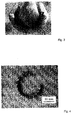
- the support structure carrying the laminate is than placed in a suitable crucible, e.g. a cut tube or half pipe as depicted in Fig. 2.
- the cut tube is provided with spacers-laminate at both ends thereof (see Fig. 3) on which the support structure is supported.
- the spacer-laminates are made of the same laminate that was used for the manufacture of the structure to be sintered. Such a spacer-laminate exhibits during sintering the same shrinking rate as the laminate. Consequently the laminate being placed on the support structure will not be pressed on the surface of the half pipe by the weight of the rod. Thereby effectively an adhesion of the sintered ceramic to the half pipe can be prevented
- the aforementioned arrangement is then placed in a furnace.
- the furnace is heated up slowly to a first temperature.
- the temperatures for burning out and sintering are selected in dependence of the used organic and ceramic components. Conventional heating profiles and atmospheres are used. - After cooling the resulting ceramic helix is pulled off from the rod.
- Ring-like helix with a curved axis as depicted in Fig. 4 can be manufactured, too by this method.
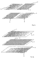
- a first metal layer 1 serving as negative electrode and a second metal layer 2 serving as ground plate are provided on the surface of an upper green layer 3.
- a lower green layer 4 is provided with in a similar design with a third metal layer 5 serving as further ground plate and a fourth metal layer 6 serving as positive electrode.
- the upper green layer 3 is stacked above the lower green layer 4 in such way that the fourth metal layer 6 is placed below the second metal layer 2 and the third metal layer 5 is placed below the first metal layer 1.
- Fig. 5b there are provided an upper 3, a middle 7 and a lower green layer 4.
- the first metal layer 1 on the upper layer 3 serves here as positive electrode and a second metal layer 2 on the middle green layer 7 as ground plate.
- the fourth metal layer 6 of the lower green layer serves here as positive electrode.
- the electrode printed has a triangle design to allow for a gradient of the electric field when a voltage is applied later on in the final product. Such electrode is used to be able to vary in one structure between contraction on one end and expansion on the other end of the final fired and poled piezoceramic.
- the green stacks are produced with a stacking pressure of 5 MPa at a lamination temperature of 120°C.
- planar stack is cut into stripes which were then wound at elevated temperatures of minimum 60°C, around Alumina cores with a thickness of 1, 3, 5 and 10mm, covered by porous polyethylene foil.
- the spiral structure is covered with a release foil to prevent sticking to the vacuum sealing bags.
- Every individual assembly is put into a vacuum-sealed bag.
- the bag is covered with a self-vulcanising silicone elastomer, which is water and temperature resistant.
- the said packages are heated in a water filled isostatic press at 155°C at 10, 20 or 40 MPa.
- a multilayer of 38 layers of Solufill based on ultrahigh molecular weight polyethylene loaded with more than 92 wt % a soft PZT fine grained piezo ceramic powder with a layer thickness of 20 microns was made by a stacking and screen-printing process (print on stack method).
- the green stacks are produced with a stacking pressure of 20MPa at a lamination temperature of 120°C.
- the planar stack is cut into stripes which then were wound at elevated temperatures of minimum 60°C, around Alumina cores with a thickness of 1, 3, 5 and 10mm, covered by porous polyethylene foil.
- the spiral structure is covered with a release foil to prevent sticking to the vacuum sealing bags.
- Every individual assembly is put into a vacuum-sealed bag.
- the bag is covered with a self-vulcanising silicone elastomer, which is water and temperature resistant.
- the said packages are heated in a water filled isostatic press at 155°C at 10, 20 or 40 MPa
- a multilayer of 20 layers of Solufill based on ultrahigh molecular weight polyethylene loaded with more than 92 wt % a soft PZT fine grained piezo ceramic powder with a layer thickness of 10 microns was made by a stacking and screen-printing process (print on stack method).
- the green stacks are produced with a stacking pressure of 5MPa at a lamination temperature of 120°C.
- the planar stack is cut into stripes which then were wound at elevated temperatures of minimum 60°C, around Alumina cores with a thickness of 1, 3, 5 and 10mm, covered by porous polyethylene foil.
- the spiral structure is covered with a release foil to prevent sticking to the vacuum sealing bags.
- Every individual assembly is put into a vacuum-sealed bag.
- the bag is covered with a self-vulcanising silicone elastomer, which is water and temperature resistant.
- the said packages are heated in a water filled isostatic press at 155°C at 10, 20 or 40 MPa.
- a multilayer of 10 layers of tape cast piezoceramic green tapes with a layer thickness of 60 ⁇ m was made by a regular screenprinting, stacking, and lamination process.
- the green tape was achieved by tape casting an organic solvent-based slurry, comprising 800g PZT-powder, 40g polyvinylbutyral as a binder and 26 g dibuthylphthalate as a plasticizer.
- the dried sheets were screen printed, stacked and pre-laminated (5 MPa, 50 °C, 5-7 min) using position holes. After cutting the planar sheets into stripes they were wound at elevated temperatures of minimum 50 °C around Alumina cores ( ⁇ 5-10 mm), covered with e.g. porous Polyethylene foil of different thickness. Every individual assembly is put in a vacuum-sealed bag, which is water and temperature resistant for the isostatic lamination process.
- the isostatic lamination is done at 70 °C and 20 MPa for 10 minutes.
- a multilayer of 10 layers of tape cast piezoceramic green tapes with a layer thickness of 90 ⁇ m was made by a regular screenprinting stacking, and lamination process.
- the green tape was achieved by tape casting an organic solvent based slurry, comprising 700 g PZT-powder, 70 g polyvinylbutyral as a binder and 70 g dibuthylphthalate as a plasticizer.
- the green tapes had a higher binder content and a higher plasticizer/binder ratio.
- the green tapes show here a strain to failure of 24%.
- the strain to failure or the longitudinal extensibility, respectively, of a green layer or green tape, respectively, was determined by conventional strain-strength measurement until failure by a mechanical testing machine at feed speed of 1 mm/min and a layer thickness of 90 ⁇ m.
- the free clamping length of the mechanical testing machine is 50 mm. The measurement is made at room temperature.
- the dried sheets were screen printed, stacked and laminated (3-5 MPa, 70 °C, 7-10 min) using position holes. After cutting the planar sheets into stripes they were wound at elevated temperatures of minimum 50 °C around Alumina cores ( ⁇ 2-5 mm) without any coverage. Every individual assembly is put in an oven (70 °C) for 5 minutes for relaxation of the wounded/twisted structure. The helixes were removed from the Alumina core material. In another step they were wounded using a special support structure to fix the shape of a curved helix during binder burnout and sintering.
- the laminate was debindered using 2 K/min to 200 °C and 0.3 K/min up to 600 °C.
- the sintering was done at 1190 °C for three hours. After sintering crack free and freestanding helixes were obtained.
Abstract
The invention relates to a method of making a layered ceramic
device comprising the steps of:

Description
The invention relates to a method of making a laminated ceramic
with a non-planar structure. More particular, the invention
concerns a method of making an electro-active device
such as piezoelectric and piezoresistive devices having a
non-planar structure.
Such electro-active devices are described for example in the
International Publication WO 01/47041 A2. The devices described
therein have been prepared mostly as bimorph devices.
Bimorph devices consist of two laminated metallized lead zirconate
titanate (PZT) layers. The manufacturing of such bimorph
devices is described in Su, B. et al., Journal of the
European Ceramic Society 21 (2001) 2005-2009. The bimorph devices
are prepared by viscous polymer processing (VPP).
Thereby a plastic ceramic mass is extruded and calendered to
sheets of 200 µm up to 2 mm thickness. The VPP-process is
limited to the manufacture of laminates comprising two green
layers, because the green layers can not be manufactured accurately
with thickness below 200 µm, the thin green layers
exhibit not a sufficiently constant thickness compared to
doctor-blade tape casting processes. Due to a high amount of
organic additives the green layers show a relatively high
shrinkage, shape instability and lack of process control.
In order to reduce the voltage supply it is desired to fabricate
non-planar structures, in particular helical structures,
from multilayer ceramic laminates made of thinner layers.
However, laminated stacks of green ceramic layers tend to
crack in particular when being formed into helical structures.
A further problem is that a predetermined exact alignment
of electrodes being applied on the layers is deorientated
by forming the laminate.
An object of the present invention is to describe a method of
making a laminated ceramic by which the disadvantages in the
art are avoided. An aim of the present invention is in particular
to provide an inexpensive and easily reproducible
method for making a laminated ceramic, in particular an electro-active
device.
This object is solved by the features of claims 1 and 4. Embodiments
of the invention are described by the features of
claims 2, 3 and 5 to 21.
According to a first aspect of the invention there is provided
a method of making an laminated ceramic with a non-planar
structure comprising the steps of:
A "laminated ceramic" in the sense of the present invention
comprises at least two ceramic layers being stacked one above
the other and being bonded together by sintering. The layers
may consist of different ceramic materials. There may be provided
in between the layers metallic layers which may act as
electrodes.
It has been surprisingly observed that an essentially planar
laminate being manufactured by a laminating step (L1) with a
relatively low pressure can be formed into a non-planar
structure respectively shape without cracking. By applying a
higher pressure and/or temperature in a subsequent further
laminating step a further densification of the formed laminate
is achieved. The non-planar structure of the laminate is
fixed. Any elastic forces induced by bending the laminate are
removed by the further laminating step (L2). This renders it
possible to manufacture laminated ceramic devices of non-planar
shape, in particular electro-active devices, in an inexpensive
and easily reproducible way.
The pressure applied in the further laminating step (L2) may
be in the range of 2 to 300 MPa. The temperature applied in
the further laminating step (L2) may be in the range of 20 to
220°C.
According to a second aspect of the invention there is provided
a method of making an laminated ceramic with a non-planar
structure comprising the steps of:
A green layer having a longitudinal extensibility of at least
17% may be manufactured by adjusting an appropriate ratio of
ceramic powder:organic binder and/or the ratio of
binder:plasticizer. The ratio/s strongly depend/s on the respective
ceramic system. Starting from a conventional composition
for a green layer of a given ceramic system one has to
increase for example step by step the content of the organic
binder until the necessary longitudinal extensibility is
achieved. Thereby it has to be taken into account that the
green density of the green layer is not lowered below a value
that affects sinterability or the density of the sintered
product.
The longitudinal extensibility of a green layer was determined
by conventional strain-strength measurement until failure
by a mechanical testing machine at feed speed of 1 mm/min
and a layer thickness of 90 µm. The free clamping length of
the mechanical testing machine is 50 mm. The measurement is
made at room temperature.
Also by the second method of the invention no cracks occur
when forming the laminate into a non-planar shape. It is assumed
that by both methods of the present invention a laminate
is provided in which the layers may be deformed plastically
during bending.
The flexible green layer may be manufactured by the doctor-blade-, ceramic-filled-thermoreversible-polymeric-gel-foil- or calendering-process. The doctor-blade-process leads to tape cast green layers. By the ceramic-filled-thermoreversible-polymeric-gel-foil-process green layers are manufactured by stretching with ceramic powder filled polyethylene films to a thickness down to 1 µm. It is referred to the U.S.-Patent No. 5,268,415 the content of which is incorporated herewith. In any case there is provided a flexible green layer comprising a ceramic powder being bound by an organic binder. The organic binder may be in general a thermoplastic or soluble polymer or a binder dispersion. The organic binder may be selected from a group consisting of cellulose ether, polymerised alcohol, polymerised butyral, acrylic resin, polyvinyl acetate and polyethylene. The organic binder may be for example methyl cellulose, polyvinyl alcohol, polyvinyl butyral, or polyvinyl metacrylate. Further the green layer may contain plasticizer. By the addition of plasticizers the glass transformation temperature of the binder is lowered. Hence, thereby the flexibility of the green layer can be adjusted. It has been observed that a ratio of binder:plasticizer in the range of 1:0,75 to 1:3,5 is advantageous. A further laminating-step (L2) (see below) after forming is not always necessary when using a higher amount of plasticizer. Further it has been observed that a green layer with a thickness of 1 to 1000 µm may be used for the manufacture of an electro-active device according to the present invention.
The flexible green layer may be manufactured by the doctor-blade-, ceramic-filled-thermoreversible-polymeric-gel-foil- or calendering-process. The doctor-blade-process leads to tape cast green layers. By the ceramic-filled-thermoreversible-polymeric-gel-foil-process green layers are manufactured by stretching with ceramic powder filled polyethylene films to a thickness down to 1 µm. It is referred to the U.S.-Patent No. 5,268,415 the content of which is incorporated herewith. In any case there is provided a flexible green layer comprising a ceramic powder being bound by an organic binder. The organic binder may be in general a thermoplastic or soluble polymer or a binder dispersion. The organic binder may be selected from a group consisting of cellulose ether, polymerised alcohol, polymerised butyral, acrylic resin, polyvinyl acetate and polyethylene. The organic binder may be for example methyl cellulose, polyvinyl alcohol, polyvinyl butyral, or polyvinyl metacrylate. Further the green layer may contain plasticizer. By the addition of plasticizers the glass transformation temperature of the binder is lowered. Hence, thereby the flexibility of the green layer can be adjusted. It has been observed that a ratio of binder:plasticizer in the range of 1:0,75 to 1:3,5 is advantageous. A further laminating-step (L2) (see below) after forming is not always necessary when using a higher amount of plasticizer. Further it has been observed that a green layer with a thickness of 1 to 1000 µm may be used for the manufacture of an electro-active device according to the present invention.
The applying of an electrode layer on the surface of the
green layers may be carried out in conventional manner. A
metal paste can be screen-printed upon the surface of the
green layer. Several electrodes may be printed on the surface
of the green layers. In particular metal pastes forming tacky
metallic layers are useful.
In order to achieve an exact alignment of the stacked green
layers it is advantageous to cut the green layers to a uniform
geometry. Further there may be provided position holes
in the green layers. Such position holes facilitate in particular
the alignment of electrodes being provided on the
surface of the green layers, when stacking the green layers.
Alternatively the green layers may be laminated on a carrier
plate in a multilayer manner. The carrier plate serves for
registration during an electrode printing step on each green
layer being added. This method is also known as "print on
stack method".
According to an essential feature of the invention the
stacked green layers are laminated in a laminating-step (L1)
before forming. The parameters of the laminating-step (L1)
are adjusted in dependence of the number of the stacked green
layers, the thickness of the green layers, the used binders,
plasticizers etc.. The resulting laminate is flexible. It can
be formed and bent with a little likelihood of cracking. It
has been observed that it is advantageous to adjust in the
laminating-step the pressure and/or temperature to create a
laminate with a porosity of at least 3,0 Vol.%. Such a laminate
may be infiltrated after the lamination step (L1) with
plasticizer. Such an infiltration with plasticizer enhances
further the flexibility of the laminate. The likelihood of
cracking during forming is further reduced. The likelihood of
cracking during forming may be also reduced when forming the
laminate at a temperature in the range of 50 to 150°C. By
heating up the laminate the viscosity of the binder is reduced.
The flexibility of the laminate is increased.
According to a further embodiment of the invention the laminate
is formed into the non-planar structure by placing it on
a support structure. The support structure may be a cylindrical
body or a body of any other cross-section. According to a
further advantageous feature the laminate is fixed on the
support structure. The fixing may be accomplished by such adhesives
that do not affect the quality of the ceramic. By
fixing the laminate on the support structure elastic forces
of the bent laminate may be compensated, which may otherwise
deform the laminate in an uncontrolled manner
According to a further embodiment a spacer made of organic
material is placed between the support structure and the
laminate. Such a spacer burns out during sintering process.
Shrinkage of the formed laminate during sintering can be successfully
compensated by the use of such a spacer. Otherwise
cracks may occur and/or the sintered ceramic can not be removed
from the support structure.
- The first and/or the second laminating step/s may be performed
by isostatic pressing.
According to a further embodiment before step 1.3 or 4.3 an
electrode layer may be applied on the surface of at least one
of the green layers. This makes it in an easy way possible to
manufacture a laminated ceramic being provided with electrodes
within the ceramic layers. Such a laminated ceramic
can be used for making electro-active devices. In the context
of the present invention "electro-active devices" are devices
which make use of components that display electro-active
properties - that is, those in which a component changes
shape in response to a change of the appropriate electrical
conditions in which the component exists. Equally, the component
may produce electrical signals in response to a shape
change. The best known and most developed of these devices
are piezoelectric devices. However, it will be understood
that there are number of other sorts of electro-active devices
including those that are electrostrictive or piezoresistive.
Electrostrictive devices are formed from a material
that contracts on the application of an electric field; piezoresistive
materials change their electrical resistance when
they change shape.
By the described method an electro-active device of non-planar
structure can be manufactured at low costs. In particular
helical structures can be realised. The electric-active
device comprises a multilayer structure with at least
2, preferably at least 10, ceramic layers. Such a device can
be operated with a low voltage supply. Helical structures
made of electro-active multilayer laminates are excellent for
the use in loudspeakers, phase shifters, optical devices
etc..
Embodiments of the invention are now described by way of non-liminative
examples with reference to the accompanying drawings
in which:
- Fig. 1
- is a flow chart illustrating the steps of a method according to the invention,
- Fig. 2
- is a photograph of a helical structure on a cylindrical support,
- Fig. 3
- is a photograph of a lateral view of a half pipe with a spacer-laminate,
- Fig. 4
- is a photograph of a sintered helical structure,
- Fig. 5a
- is a drawing of a first electrode design, and
- Fig. 5b
- is a drawing of a second electrode design.
Fig. 1 shows a flow chart of a method according to the invention.
A conventional flexible green layer manufactured i.e.
by tape casting is provided. The green layer may comprise essentially
a PZT-powder being bound by polyvinyl butyral containing
a conventional plasticizer. The green layer can contain
also as ceramic component any other material that exhibits
in the sintered state i.e. piezoelectric, electrostrictive
or piezoresistive properties.
The green layer is then cut in sheets of a predetermined geometry.
Position holes are punched into the sheets. Then metallic
layers are applied upon the surface of the sheets,
i.e. by screen-printing of conventional metal pastes. The metallic
layers form several electrodes on the surface. The
sheets are stacked one upon the other using the position
holes. In the stacked state the electrodes are in precise
alignment. This allows a contacting of the electrodes as well
as the application of terminals in a conventional manner.
The stack is then "pre-laminated" in a first laminating step (L1) by applying an uniaxial or isostatic pressure in the range of 0,2 to 20 MPa and a temperature of typically 50 to 135°C. The applied pressure and temperature depends essentially on the organic components used for the manufacture of the green layers.
The stack is then "pre-laminated" in a first laminating step (L1) by applying an uniaxial or isostatic pressure in the range of 0,2 to 20 MPa and a temperature of typically 50 to 135°C. The applied pressure and temperature depends essentially on the organic components used for the manufacture of the green layers.
However, it has been observed that it is advantageous to select
the pressure and the temperature parameters so that the
resulting laminate exhibits a porosity of more than 3,0
Vol.%. Such a laminate can be formed into a wide range in
non-planar shapes without cracking. The laminate is typically
made of about 20 to 100 green layers with a thickness of 1 to
200 µm.
The laminated sheets are cut into stripes. For forming purposes
a support structure, i.e. a rod made of ceramic material
is provided.
It has been observed that it is advantageous to provide a
support structure with a smooth surface in order to minimise
friction during the shrinkage of the ceramic during sintering.
A smooth surface of the support structure also allows
removing the sintered ceramic easily after sintering has been
completed. It has been found advantages to choose a roughness
value RA for the surface smaller or equal 2 µm. More preferably
the roughness value may be chosen smaller than 1/3 of the
average grain size of the ceramic powder.
The rod is coated with a spacer-layer made of organic material.
Such a spacer-layer may be applied by dipping the rod
in a solution containing a polymer and a solvent. The thickness
of the spacer-layer can be adjusted by the number of
dippings and/or by the concentration of the solution. The
spacer-layer may also be applied by spraying. As material for
the spacer-layer an organic material is used which burns out
without affecting the properties of the ceramic.
One of the stripes is then wound around the rod so that a
helical structure is formed. The stripe may by fixed upon the
rod, i.e. by using an adhesive, i.e. a double- or mono-sided
adhesive tape. The stripe may also heated up to a temperature
between 50°C and 150°C, typically 70°C, before forming.
Thereby the flexibility, in particular the winding behaviour,
of the stripe is improved.
Afterwards the laminate being placed on the support structure
is further densified by isostatic pressing in a second laminating
step (L2). The support structure with the laminate is
vacuum-sealed in plastic bag or the like and than placed in
an isostatic press. A pressure of 10 to 40 MPa and a temperature
of about 130 to 180°C are applied. - It has to be understood
that this second laminating step (L2) is an optional
step, which improves usually the quality of the sintered ceramic.
However, it has been observed that also without carrying
out this second laminating step (L2) good results can be
achieved.
The support structure carrying the laminate is than placed in
a suitable crucible, e.g. a cut tube or half pipe as depicted
in Fig. 2. The cut tube is provided with spacers-laminate at
both ends thereof (see Fig. 3) on which the support structure
is supported. The spacer-laminates are made of the same laminate
that was used for the manufacture of the structure to be
sintered. Such a spacer-laminate exhibits during sintering
the same shrinking rate as the laminate. Consequently the
laminate being placed on the support structure will not be
pressed on the surface of the half pipe by the weight of the
rod. Thereby effectively an adhesion of the sintered ceramic
to the half pipe can be prevented
The aforementioned arrangement is then placed in a furnace.
The furnace is heated up slowly to a first temperature.
Thereby the organic components of the laminate and the
spacer-layer burn out. After burning-out is completed the
temperature is risen upon sintering temperature. The temperatures
for burning out and sintering are selected in dependence
of the used organic and ceramic components. Conventional
heating profiles and atmospheres are used. - After cooling
the resulting ceramic helix is pulled off from the rod.
Ring-like helix with a curved axis as depicted in Fig. 4 can
be manufactured, too by this method.
In Fig. 5a and 5b embodiments of electrode design are depicted.
In Fig. 5a a first metal layer 1 serving as negative
electrode and a second metal layer 2 serving as ground plate
are provided on the surface of an upper green layer 3. A
lower green layer 4 is provided with in a similar design with
a third metal layer 5 serving as further ground plate and a
fourth metal layer 6 serving as positive electrode. The upper
green layer 3 is stacked above the lower green layer 4 in
such way that the fourth metal layer 6 is placed below the
second metal layer 2 and the third metal layer 5 is placed
below the first metal layer 1.
In Fig. 5b there are provided an upper 3, a middle 7 and a
lower green layer 4. The first metal layer 1 on the upper
layer 3 serves here as positive electrode and a second metal
layer 2 on the middle green layer 7 as ground plate. The
fourth metal layer 6 of the lower green layer serves here as
positive electrode.
The method according to the invention is now described in
more detail by way of the following examples:
A multilayer of 38 layers of Solufill based on ultrahigh molecular
weight polyethylene loaded with more than 92 wt % a
soft PZT fine grained piezo ceramic powder with a layer
thickness of 20 µm was made by a stacking and screenprinting
process (="print on stack method"). The electrode printed has
a triangle design to allow for a gradient of the electric
field when a voltage is applied later on in the final product.
Such electrode is used to be able to vary in one structure
between contraction on one end and expansion on the
other end of the final fired and poled piezoceramic. The
green stacks are produced with a stacking pressure of 5 MPa
at a lamination temperature of 120°C. The planar stack is cut
into stripes which were then wound at elevated temperatures
of minimum 60°C, around Alumina cores with a thickness of 1,
3, 5 and 10mm, covered by porous polyethylene foil. The spiral
structure is covered with a release foil to prevent
sticking to the vacuum sealing bags.
Every individual assembly is put into a vacuum-sealed bag.
The bag is covered with a self-vulcanising silicone elastomer,
which is water and temperature resistant. The said
packages are heated in a water filled isostatic press at
155°C at 10, 20 or 40 MPa.
A multilayer of 38 layers of Solufill based on ultrahigh molecular
weight polyethylene loaded with more than 92 wt % a
soft PZT fine grained piezo ceramic powder with a layer
thickness of 20 microns was made by a stacking and screen-printing
process (print on stack method). The green stacks
are produced with a stacking pressure of 20MPa at a lamination
temperature of 120°C. The planar stack is cut into
stripes which then were wound at elevated temperatures of
minimum 60°C, around Alumina cores with a thickness of 1, 3,
5 and 10mm, covered by porous polyethylene foil. The spiral
structure is covered with a release foil to prevent sticking
to the vacuum sealing bags.
Every individual assembly is put into a vacuum-sealed bag.
The bag is covered with a self-vulcanising silicone elastomer,
which is water and temperature resistant. The said
packages are heated in a water filled isostatic press at
155°C at 10, 20 or 40 MPa
A multilayer of 20 layers of Solufill based on ultrahigh molecular
weight polyethylene loaded with more than 92 wt % a
soft PZT fine grained piezo ceramic powder with a layer
thickness of 10 microns was made by a stacking and screen-printing
process (print on stack method). The green stacks
are produced with a stacking pressure of 5MPa at a lamination
temperature of 120°C. The planar stack is cut into stripes
which then were wound at elevated temperatures of minimum
60°C, around Alumina cores with a thickness of 1, 3, 5 and
10mm, covered by porous polyethylene foil. The spiral structure
is covered with a release foil to prevent sticking to
the vacuum sealing bags.
Every individual assembly is put into a vacuum-sealed bag.
The bag is covered with a self-vulcanising silicone elastomer,
which is water and temperature resistant. The said
packages are heated in a water filled isostatic press at
155°C at 10, 20 or 40 MPa.
A multilayer of 10 layers of tape cast piezoceramic green
tapes with a layer thickness of 60 µm was made by a regular
screenprinting, stacking, and lamination process. The green
tape was achieved by tape casting an organic solvent-based
slurry, comprising 800g PZT-powder, 40g polyvinylbutyral as
a binder and 26 g dibuthylphthalate as a plasticizer. The
dried sheets were screen printed, stacked and pre-laminated
(5 MPa, 50 °C, 5-7 min) using position holes. After cutting
the planar sheets into stripes they were wound at elevated
temperatures of minimum 50 °C around Alumina cores (⊘ 5-10
mm), covered with e.g. porous Polyethylene foil of different
thickness. Every individual assembly is put in a vacuum-sealed
bag, which is water and temperature resistant for the
isostatic lamination process. The isostatic lamination is
done at 70 °C and 20 MPa for 10 minutes.
A multilayer of 10 layers of tape cast piezoceramic green
tapes with a layer thickness of 90 µm was made by a regular
screenprinting stacking, and lamination process. The green
tape was achieved by tape casting an organic solvent based
slurry, comprising 700 g PZT-powder, 70 g polyvinylbutyral as
a binder and 70 g dibuthylphthalate as a plasticizer.
In contrast to example 4, the green tapes had a higher binder
content and a higher plasticizer/binder ratio. The green
tapes show here a strain to failure of 24%. The strain to
failure or the longitudinal extensibility, respectively, of a
green layer or green tape, respectively, was determined by
conventional strain-strength measurement until failure by a
mechanical testing machine at feed speed of 1 mm/min and a
layer thickness of 90 µm. The free clamping length of the mechanical
testing machine is 50 mm. The measurement is made at
room temperature.
The dried sheets were screen printed, stacked and laminated
(3-5 MPa, 70 °C, 7-10 min) using position holes. After cutting
the planar sheets into stripes they were wound at elevated
temperatures of minimum 50 °C around Alumina cores (⊘
2-5 mm) without any coverage. Every individual assembly is
put in an oven (70 °C) for 5 minutes for relaxation of the
wounded/twisted structure. The helixes were removed from the
Alumina core material. In another step they were wounded using
a special support structure to fix the shape of a curved
helix during binder burnout and sintering.
In all examples the laminate was debindered using 2 K/min to
200 °C and 0.3 K/min up to 600 °C. The sintering was done at
1190 °C for three hours. After sintering crack free and freestanding
helixes were obtained.
Claims (21)
- A method of making an laminated ceramic with a non-planar structure comprising the steps of:1.1 providing flexible green layers comprising a ceramic powder being bound by an organic binder,1.2 stacking of the green layers,1.3 laminating of the stacked green layers in a laminating step (L1) by applying a pressure in the range of 0,2 to 25 MPa and a temperature in the range of 20 to 220°C,1.4 forming the laminate into a non-planar structure,1.5 laminating the formed laminate in a further laminating step (L2), wherein in the further laminating step (L2) a pressure being higher than the pressure applied in the laminating step (L1) and/or a temperature being higher than the temperature applied the laminating step (L1) is applied, and1.6 burning out of the organic binder and sintering.
- A method of claim 1 wherein the pressure applied in the further laminating step (L2) is in the range of 2 to 300 MPa.
- A method of one of the preceding claims wherein the temperature applied in the further laminating step (L2) is in the range of 20 to 220°C.
- A method of making an laminated ceramic with a non-planar structure comprising the steps of:4.1 providing flexible green layers comprising a ceramic powder being bound by a organic binder, wherein the green layer has a longitudinal extensibility of at least 17%,4.2 stacking of the green layers,4.3 laminating of the stacked green layers in a laminating step (L1) by applying a pressure in the range of 0,2 to 300 MPa and a temperature in the range of 20 to 220°C,4.4 forming the laminate into a non-planar structure, and4.5 burning out of the organic binder and sintering.
- A method of one of the preceding claims wherein the flexible green layer is manufactured by the doctor-blade-, ceramic-filled-thermoreversible-polymeric-gel-foil- or calendering-process.
- A method of one of the preceding claims wherein the organic binder is selected form a group consisting of e.g. cellulose ether, polymerised alcohol, polymerised butyrol, acrylic resin, polyvinylacetate, polyethylene.
- A method of one of the preceding claims wherein the green layer contains plasticizer.
- A method of one of the preceding claims wherein the ratio of binder:plasticizer is in the range of 1:0,75 to 1:3,5.
- A method of one of the preceding claims wherein the green layer has a thickness of 1 to 1000µm.
- A method of one of the preceding claims wherein in the laminating step the pressure and/or temperature is adjusted to create a laminate with a porosity of at least 3,0 Vol.%
- A method of one of the preceding claims wherein the pore space of the laminate is infiltrated with plasticizer before forming.
- A method of one of the preceding claims wherein the laminate is formed at a temperature in the range of 50 to 150°C.
- A method of one of the preceding claims wherein the laminate is formed into the non-planar structure by placing it on a support structure.
- A method of one of the preceding claims wherein the laminate is fixed on the support structure, preferably by an adhesive tape.
- A method of one of the preceding claims wherein a spacer made of organic material is placed between the support structure and the laminate.
- A method of one of the preceding claims wherein the pressure in the laminating step (L1) and/or the further laminating step (L2) is performed by isostatic pressing.
- A method of one of the preceding claims wherein before step 1.3 or 4.3 an electrode layer is applied on the surface of at least one of the green layers.
- A layered ceramic device manufactured in accordance with a method of one of the preceding claims.
- A layered ceramic device of claim 18 wherein the non-planar structure is a helical structure, preferably a structure with a curved helix-axis.
- A layered ceramic device of claim 18 or 19 wherein the laminate comprises at least 2, preferably at least 10, ceramic layers.
- A layered ceramic device of one of claims 18 to 20 being made of an electro-active ceramic material.
Priority Applications (1)
| Application Number | Priority Date | Filing Date | Title |
|---|---|---|---|
| EP02023464A EP1416546A1 (en) | 2002-10-21 | 2002-10-21 | Method of making a laminated ceramic with a non-planar structure |
Applications Claiming Priority (1)
| Application Number | Priority Date | Filing Date | Title |
|---|---|---|---|
| EP02023464A EP1416546A1 (en) | 2002-10-21 | 2002-10-21 | Method of making a laminated ceramic with a non-planar structure |
Publications (1)
| Publication Number | Publication Date |
|---|---|
| EP1416546A1 true EP1416546A1 (en) | 2004-05-06 |
Family
ID=32087948
Family Applications (1)
| Application Number | Title | Priority Date | Filing Date |
|---|---|---|---|
| EP02023464A Withdrawn EP1416546A1 (en) | 2002-10-21 | 2002-10-21 | Method of making a laminated ceramic with a non-planar structure |
Country Status (1)
| Country | Link |
|---|---|
| EP (1) | EP1416546A1 (en) |
Cited By (3)
| Publication number | Priority date | Publication date | Assignee | Title |
|---|---|---|---|---|
| DE102008029426A1 (en) * | 2008-06-23 | 2010-01-07 | Epcos Ag | Method for producing a multilayer component, multilayer component and template |
| WO2013037559A1 (en) | 2011-09-15 | 2013-03-21 | Epcos Ag | Multi-layer component and method for producing same |
| US10026719B2 (en) | 2015-12-04 | 2018-07-17 | Teledyne Reynolds, Inc. | Electronic assemblies including electronic devices mounted on non-planar subrates |
Citations (5)
| Publication number | Priority date | Publication date | Assignee | Title |
|---|---|---|---|---|
| EP0425148A2 (en) * | 1989-10-23 | 1991-05-02 | AT&T Corp. | Method of forming multilayer thick film circuits |
| US5028473A (en) * | 1989-10-02 | 1991-07-02 | Hughes Aircraft Company | Three dimensional microcircuit structure and process for fabricating the same from ceramic tape |
| GB2255451A (en) * | 1991-05-03 | 1992-11-04 | Marconi Gec Ltd | Ceramic three dimensional electronic structures |
| WO2001047041A2 (en) * | 1999-12-21 | 2001-06-28 | 1... Limited | Electro-active devices |
| US20020146523A1 (en) * | 2001-04-05 | 2002-10-10 | Devoe Alan D. | Laminate thin-wall ceramic tubes, including with integral stress wrappings, thickened ends and/or internal baffles, particularly for solid oxide fuel cells |
-
2002
- 2002-10-21 EP EP02023464A patent/EP1416546A1/en not_active Withdrawn
Patent Citations (5)
| Publication number | Priority date | Publication date | Assignee | Title |
|---|---|---|---|---|
| US5028473A (en) * | 1989-10-02 | 1991-07-02 | Hughes Aircraft Company | Three dimensional microcircuit structure and process for fabricating the same from ceramic tape |
| EP0425148A2 (en) * | 1989-10-23 | 1991-05-02 | AT&T Corp. | Method of forming multilayer thick film circuits |
| GB2255451A (en) * | 1991-05-03 | 1992-11-04 | Marconi Gec Ltd | Ceramic three dimensional electronic structures |
| WO2001047041A2 (en) * | 1999-12-21 | 2001-06-28 | 1... Limited | Electro-active devices |
| US20020146523A1 (en) * | 2001-04-05 | 2002-10-10 | Devoe Alan D. | Laminate thin-wall ceramic tubes, including with integral stress wrappings, thickened ends and/or internal baffles, particularly for solid oxide fuel cells |
Non-Patent Citations (2)
| Title |
|---|
| LODGE J ET AL: "Ceramic electronic substrates move into three dimensions", PROCEEDINGS OF THE 1995 INTERNATIONAL ELECTRONICS PACKAGING CONFERENCE, PROCEEDINGS OF 1995 INTERNATIONAL ELECTRONICS PACKAGING CONFERENCE, SAN DIEGO, CA, USA, 24-27 SEPT. 1995, 1995, Wheaton, IL, USA, Int. Electron. Packaging Soc, USA, pages 461 - 472, XP008015784 * |
| SU B ET AL: "Routes to net shape electroceramic devices and thick films", JOURNAL OF THE EUROPEAN CERAMIC SOCIETY, ELSEVIER SCIENCE PUBLISHERS, BARKING, ESSEX, GB, vol. 21, no. 10-11, 2001, pages 2005 - 2009, XP004301817, ISSN: 0955-2219 * |
Cited By (7)
| Publication number | Priority date | Publication date | Assignee | Title |
|---|---|---|---|---|
| DE102008029426A1 (en) * | 2008-06-23 | 2010-01-07 | Epcos Ag | Method for producing a multilayer component, multilayer component and template |
| WO2013037559A1 (en) | 2011-09-15 | 2013-03-21 | Epcos Ag | Multi-layer component and method for producing same |
| DE102011113496A1 (en) | 2011-09-15 | 2013-03-21 | Epcos Ag | Multi-layer component and method for its production |
| CN103797553A (en) * | 2011-09-15 | 2014-05-14 | 埃普科斯股份有限公司 | Multi-layer component and method for producing same |
| JP2014531130A (en) * | 2011-09-15 | 2014-11-20 | エプコス アクチエンゲゼルシャフトEpcos Ag | Multilayer device and manufacturing method thereof |
| US9583262B2 (en) | 2011-09-15 | 2017-02-28 | Epcos Ag | Multi-layer component and method for producing same |
| US10026719B2 (en) | 2015-12-04 | 2018-07-17 | Teledyne Reynolds, Inc. | Electronic assemblies including electronic devices mounted on non-planar subrates |
Similar Documents
| Publication | Publication Date | Title |
|---|---|---|
| KR100394349B1 (en) | Monolithic ceramic electronic component and production process therefor, and ceramic paste and production process therefor | |
| JP5341094B2 (en) | Multilayer piezoelectric element, injection device, and fuel injection system | |
| US6931713B2 (en) | Methods of making low loss, high frequency composite magnetic material | |
| US6607690B2 (en) | Methods for manufacturing ceramic green sheet and multilayer ceramic electronic parts | |
| JP2010520633A (en) | Piezoelectric composite material | |
| CN106032326B (en) | Multilayer composite ceramic plate and preparation method thereof | |
| EP1416546A1 (en) | Method of making a laminated ceramic with a non-planar structure | |
| WO2005041316A1 (en) | Multilayer piezoelectric device | |
| JPWO2003036667A1 (en) | Manufacturing method of multilayer ceramic electronic component | |
| WO2004088686A1 (en) | Production method for laminated ceramic electronic component | |
| Wagner et al. | Novel low voltage piezoactuators for high displacements | |
| JP4373643B2 (en) | LAMINATED PIEZOELECTRIC ELEMENT, ITS MANUFACTURING METHOD, AND INJECTION DEVICE | |
| JPWO2004101465A1 (en) | CERAMIC GREEN SHEET AND MULTILAYER CERAMIC ARTICLE AND METHOD FOR PRODUCING THE SAME | |
| KR20050061910A (en) | Actuator and method for fabrication thereof | |
| JP3006518B2 (en) | Multilayer ceramic electronic component and method of manufacturing the same | |
| JP3603655B2 (en) | Conductive paste and method for manufacturing ceramic electronic component using the same | |
| JP4941915B2 (en) | Manufacturing method of ceramic green sheet | |
| KR100930176B1 (en) | Ceramic substrate and its manufacturing method | |
| JP2011061190A (en) | Method of manufacturing composite electronic component and composite electronic component | |
| EP1158549A1 (en) | Laminated body manufacturing method and laminated body pressurizing device | |
| KR20010006441A (en) | Method and apparatus for producing multilayer body for electronic component | |
| CN106032076B (en) | Ceramic-based metamaterial and preparation method thereof | |
| JP4439257B2 (en) | Ceramic green sheet and manufacturing method thereof | |
| JP2004168556A (en) | Ceramic green sheet and method of manufacturing the same | |
| JP4868707B2 (en) | Multilayer piezoelectric element and injection device |
Legal Events
| Date | Code | Title | Description |
|---|---|---|---|
| PUAI | Public reference made under article 153(3) epc to a published international application that has entered the european phase |
Free format text: ORIGINAL CODE: 0009012 |
|
| AK | Designated contracting states |
Kind code of ref document: A1 Designated state(s): AT BE BG CH CY CZ DE DK EE ES FI FR GB GR IE IT LI LU MC NL PT SE SK TR |
|
| AX | Request for extension of the european patent |
Extension state: AL LT LV MK RO SI |
|
| AKX | Designation fees paid | ||
| REG | Reference to a national code |
Ref country code: DE Ref legal event code: 8566 |
|
| STAA | Information on the status of an ep patent application or granted ep patent |
Free format text: STATUS: THE APPLICATION IS DEEMED TO BE WITHDRAWN |
|
| 18D | Application deemed to be withdrawn |
Effective date: 20041109 |