EP1416509A1 - Production method for spacer assembly used in flat display unit - Google Patents
Production method for spacer assembly used in flat display unit Download PDFInfo
- Publication number
- EP1416509A1 EP1416509A1 EP02746063A EP02746063A EP1416509A1 EP 1416509 A1 EP1416509 A1 EP 1416509A1 EP 02746063 A EP02746063 A EP 02746063A EP 02746063 A EP02746063 A EP 02746063A EP 1416509 A1 EP1416509 A1 EP 1416509A1
- Authority
- EP
- European Patent Office
- Prior art keywords
- spacer
- forming material
- grid
- temperature
- holes
- Prior art date
- Legal status (The legal status is an assumption and is not a legal conclusion. Google has not performed a legal analysis and makes no representation as to the accuracy of the status listed.)
- Withdrawn
Links
Images




Classifications
-
- H—ELECTRICITY
- H01—ELECTRIC ELEMENTS
- H01J—ELECTRIC DISCHARGE TUBES OR DISCHARGE LAMPS
- H01J29/00—Details of cathode-ray tubes or of electron-beam tubes of the types covered by group H01J31/00
- H01J29/02—Electrodes; Screens; Mounting, supporting, spacing or insulating thereof
- H01J29/028—Mounting or supporting arrangements for flat panel cathode ray tubes, e.g. spacers particularly relating to electrodes
-
- H—ELECTRICITY
- H01—ELECTRIC ELEMENTS
- H01J—ELECTRIC DISCHARGE TUBES OR DISCHARGE LAMPS
- H01J31/00—Cathode ray tubes; Electron beam tubes
- H01J31/08—Cathode ray tubes; Electron beam tubes having a screen on or from which an image or pattern is formed, picked up, converted, or stored
- H01J31/10—Image or pattern display tubes, i.e. having electrical input and optical output; Flying-spot tubes for scanning purposes
- H01J31/12—Image or pattern display tubes, i.e. having electrical input and optical output; Flying-spot tubes for scanning purposes with luminescent screen
- H01J31/123—Flat display tubes
- H01J31/125—Flat display tubes provided with control means permitting the electron beam to reach selected parts of the screen, e.g. digital selection
- H01J31/127—Flat display tubes provided with control means permitting the electron beam to reach selected parts of the screen, e.g. digital selection using large area or array sources, i.e. essentially a source for each pixel group
-
- H—ELECTRICITY
- H01—ELECTRIC ELEMENTS
- H01J—ELECTRIC DISCHARGE TUBES OR DISCHARGE LAMPS
- H01J9/00—Apparatus or processes specially adapted for the manufacture, installation, removal, maintenance of electric discharge tubes, discharge lamps, or parts thereof; Recovery of material from discharge tubes or lamps
- H01J9/02—Manufacture of electrodes or electrode systems
- H01J9/18—Assembling together the component parts of electrode systems
- H01J9/185—Assembling together the component parts of electrode systems of flat panel display devices, e.g. by using spacers
-
- H—ELECTRICITY
- H01—ELECTRIC ELEMENTS
- H01J—ELECTRIC DISCHARGE TUBES OR DISCHARGE LAMPS
- H01J9/00—Apparatus or processes specially adapted for the manufacture, installation, removal, maintenance of electric discharge tubes, discharge lamps, or parts thereof; Recovery of material from discharge tubes or lamps
- H01J9/24—Manufacture or joining of vessels, leading-in conductors or bases
- H01J9/241—Manufacture or joining of vessels, leading-in conductors or bases the vessel being for a flat panel display
- H01J9/242—Spacers between faceplate and backplate
-
- H—ELECTRICITY
- H01—ELECTRIC ELEMENTS
- H01J—ELECTRIC DISCHARGE TUBES OR DISCHARGE LAMPS
- H01J2329/00—Electron emission display panels, e.g. field emission display panels
- H01J2329/86—Vessels
- H01J2329/8625—Spacing members
- H01J2329/863—Spacing members characterised by the form or structure
-
- H—ELECTRICITY
- H01—ELECTRIC ELEMENTS
- H01J—ELECTRIC DISCHARGE TUBES OR DISCHARGE LAMPS
- H01J2329/00—Electron emission display panels, e.g. field emission display panels
- H01J2329/86—Vessels
- H01J2329/8625—Spacing members
- H01J2329/864—Spacing members characterised by the material
Definitions
- first and second dies 32 and 33 which function as molding dies, individually, are formed having a plurality of through holes 34 that correspond individually to the spacer apertures 28 of the grid 24.
- the first die 32 is formed by laminating a plurality of thin metal sheets, e.g., three thin metal sheets 32a, 32b and 32c, to one another.
- the spacer forming material is not limited to the aforementioned glass paste, and may be suitably selected as required.
- the diameter and height of the spacers and the dimensions, material, etc. of the other components may be suitably selected as required.
- the shape of each spacer is not limited to the shape of a stepped truncated cone, and may alternatively be the shape of a truncated cone without steps or any other shape.
- the parting agent may be a material that consists mainly of a binder or organic component contained by the spacer forming material and is pyrolized at a lower temperature than the organic component is, and can be selected suitably.
Landscapes
- Engineering & Computer Science (AREA)
- Manufacturing & Machinery (AREA)
- Manufacture Of Electron Tubes, Discharge Lamp Vessels, Lead-In Wires, And The Like (AREA)
- Vessels, Lead-In Wires, Accessory Apparatuses For Cathode-Ray Tubes (AREA)
- Cathode-Ray Tubes And Fluorescent Screens For Display (AREA)
- Liquid Crystal (AREA)
Abstract
A spacer assembly 22 has first and second spacers
30a and 30b that are set up integrally on first and
second surfaces, respectively, of a substrate 24. Each
spacer is tapered toward its extended end. In forming
the spacer assembly, first and second molding dies
having through holes coated with a parting agent that
contains an organic component are prepared, and these
molding dies are located on the first and second
surfaces of the substrate so as to be intimately in
contact with them, individually. Thereafter, a spacer
forming material is filled into the through holes of
the molding dies and cured, whereupon the first and
second spacers are formed integrally on the substrate
surfaces.
Description
This invention relates to a method of
manufacturing a spacer assembly used in a flat display
device.
A field emission display (FED), plasma display
(PDP), etc. are known as modern flat display devices.
A display that uses a surface-conduction electron
source (hereinafter referred to as SED) is being
developed as an FED of a kind.
This SED has a faceplate and a rear plate that are
opposed to each other with a given gap between them.
These plates have their respective peripheral edge
portions jointed together by a rectangular frame-shaped
sidewall, thus forming a vacuum envelope. Phosphor
layers that glow in three colors are formed on the
inner surface of the faceplate. Arranged on the inner
surface of the rear plate are a number of emitters that
correspond individually to pixels as electron emitting
sources for exciting the phosphor. Each emitter is
composed of an electron emitting portion, a pair of
electrodes that apply voltage to the electron emitting
portion, etc.
Further, a plate-shaped grid is located between
the two plates. The grid is formed having a number of
apertures that are aligned with the emitters. Spacers
that maintain the gap between the plates are located on
the grid. An electron beam that is emitted from each
emitter is transmitted through its corresponding
aperture of the grid and applied to a desired phosphor
layer.
An SED described in U.S. Pat. No. 5,846,205 is
known as a version that has a spacer assembly formed of
a grid and spacers that resembles the ones described
above. According to this SED, the plate-shaped grid
has a number of spacer apertures, and columnar spacers
that are a little smaller in diameter than the spacer
apertures are passed through the spacer apertures,
individually, and are fixedly bonded to the grid with
an adhesive agent, frit, solder, or the like. Each
spacer projects from both sides of the grid, and its
opposite ends engage the respective inner surfaces of
a faceplate and a rear plate, individually.
The manufacture of the spacer assembly is very
troublesome, however, if it is done by passing the
columnar spacers individually into a number of spacer
apertures in the grid and fixing them with the adhesive
agent or the like in the aforesaid manner, and it is
hard to improve the manufacturing efficiency in this
case. More specifically, each spacer is very small,
having a diameter of hundreds of micrometers and a
height of several millimeters, and its corresponding
spacer aperture is also very small. Accurately
inserting the very small spacers into the spacer
apertures of the grid and fixedly bonding them to the
grid with the adhesive agent or the like require high
assembly accuracy and entail very hard operations.
Further, the manufacturing cost is increased, and the
manufacturing efficiency is lowered.
In order to reduce the movement of the electron
beams, moreover, the spacers should be thinned, and the
ratio between the diameter and height, that is, aspect
ratio (height/diameter), should be heightened. It is
hard, however, to manufacture spacers with high aspect
ratios.
This invention has been made in consideration of
these circumstances, and its object is to provide a
method of manufacturing a spacer assembly, capable of
easily manufacturing a spacer assembly of a flat
display device.
In order to achieve the above object, according to
an aspect of this invention, there is provided a method
of manufacturing a spacer assembly, which has a
substrate and a plurality of columnar spacers provided
on the substrate and is used in a flat display device,
the method comprising: preparing the substrate and a
molding die having a plurality of through holes;
forming an organic coating film by applying a parting
agent at least to the respective inner surfaces of the
through holes of the molding die, the parting agent
containing an organic component which is dissipated by
being decomposed or burned by heating at a given
temperature; locating the molding die on the surface of
the substrate so as to be intimately in contact
therewith and then filling a spacer forming material
into the through holes of the molding die; curing the
filled spacer forming material and then heating the
substrate and the molding die at a first temperature to
decompose or burn at least the organic coating film on
the respective inner surfaces of the through holes of
the molding die, thereby dissipating the organic
coating film; then parting the molding die from the
substrate; heating the spacer forming material at a
second temperature higher than the first temperature,
thereby removing a binder from the spacer forming
material, after the molding die is parted; and firing
the spacer forming material at a third temperature
higher than the first and second temperatures, thereby
forming the spacers integrally on the substrate, after
the binder removing process.
Further, according to an aspect of this invention,
there is provided a method of manufacturing a spacer
assembly, which has a plate-shaped grid having a number
of beam passage apertures and a plurality of columnar
spacers provided integrally on the grid and is used in
a flat display device, the method comprising: preparing
the plate-shaped grid having first and second surfaces
and a plurality of spacer apertures situated
individually between the beam passage apertures;
preparing first and second plate-shaped molding dies
having a plurality of through holes each; forming
organic coating films individually by applying a
parting agent at least to the respective inner surfaces
of the through holes of the first and second molding
dies, the parting agent containing an organic component
which is dissipated by being decomposed or burned by
heating at a given temperature; locating the first and
second molding dies on the first and second surfaces,
respectively, of the grid so as to be intimately in
contact therewith and so that the spacer apertures of
the grid and the through holes of the first and second
molding dies are in alignment with one another and then
filling the spacer forming material into the through
holes of the first and second molding dies and the
spacer apertures; curing the filled spacer forming
material and then heating the grid and the first and
second molding dies at a first temperature to decompose
or burn at least the organic coating films on the
respective inner surfaces of the through holes of the
first and second molding dies, thereby dissipating the
organic coating films, and parting the first and second
molding dies from the grid thereafter; heating the
spacer forming material at a second temperature higher
than the first temperature, thereby removing a binder
from the spacer forming material, after the first and
second molding dies are parted; and firing the spacer
forming material at a third temperature higher than the
first and second temperatures, thereby forming the
spacers integrally on the first and second surfaces of
the grid, after the binder removing process.
According to the method of manufacturing a spacer
assembly arranged in this manner, a plurality of
spacers can be set at a time in given positions on the
substrate or the grid by curing the spacer forming
material that is located on the substrate or the grid
by means of the molding dies. After the spacer forming
material is cured, moreover, the molding dies are
heated so that the organic coating films of the parting
agent are dissipated by heat decomposition or
combustion. Thereupon, gaps are formed between the
cured spacer forming material and the molding dies, so
that the molding dies can be easily parted from each
other. After the molding dies are parted, the binder
removing process and firing are carried out with the
cured spacer forming material exposed. By doing this,
the spacer forming material can be heated and fired
uniformly and efficiently. In consequence, the spacers
with the uniform shape, strength, etc. can be obtained.
According to the method of manufacturing a spacer
assembly of the present invention, the molding dies are
parted from each other when the spacer forming material
is subjected to the binder removing and firing, so that
the heat resistance of the molding dies can be lowered.
Thus, the molding dies can be repeatedly used with less
oxidation and deformation, so that the cost of the
molding dies can be reduced considerably.
According to the method of manufacturing a spacer
assembly of the present invention, moreover, the
diameter of each spacer is adjusted by regulating the
thickness of the organic coating film. Thus, according
to this manufacturing method, the diameter of each
spacer can be easily reduced by adjusting the thickness
of the organic coating film or by increasing the film
thickness, for example, so that the resulting spacer
assembly can have the spacers with a high aspect ratio.
An embodiment in which this invention is applied
to an SED will now be described in detail with
reference to the drawings.
As shown in FIGS. 1 to 3, this SED comprises
a rear plate 10 and a faceplate 12, which are formed of
a rectangular glass plate as a transparent insulating
substrate each. These plates are opposed to each other
with a gap of about 1.5 to 3.0 mm between them. The
rear plate 10 has a size a little larger than that of
the faceplate 12. The rear plate 10 and the faceplate
12 have their respective peripheral edge portions
jointed together by means of a glass sidewall 14 in the
form of a rectangular frame, thus forming a flat
rectangular vacuum envelope 15.
A phosphor screen 16 is formed on the inner
surface of the faceplate 12. The phosphor screen 16
has phosphor layers, which glow red, blue, and green,
individually, and a black colored layer, which are
arranged side by side. These phosphor layers are
stripe- or dot-shaped. Further, a metal back 17 of
aluminum or the like is formed on the phosphor
screen 16. A transparent electrically conductive
film of ITO or the like, or color filter film may be
provided between the faceplate 12 and the phosphor
screen.
Provided on the inner surface of the rear plate 10
are a number of surface-conduction electron emitting
elements 18 that individually emit electron beams, as
electron emitting sources for exciting the phosphor
layers. These electron emitting elements 18 are
arranged in a plurality of columns and a plurality of
rows corresponding individually to pixels. Each
electron emitting element 18 is composed of an electron
emitting portion (not shown), a pair of element
electrodes that apply voltage to the electron emitting
portion, etc. Further, a number of wires (not shown)
for applying voltage to the electron emitting elements
18 are arranged in a matrix on the rear plate 10.
The sidewall 14 that functions as a joint member
is sealed to the respective peripheral end portions of
the rear plate 10 and the faceplate 12 with a sealant
20, such as low-melting glass, low-melting metal, etc.,
thereby jointing the faceplate and the rear plate to
each other.
As shown in FIGS. 2 and 3, moreover, the SED is
provided with a spacer assembly 22 that is located
between the rear plate 10 and the faceplate 12. In the
present embodiment, the spacer assembly 22 includes
a plate-shaped grid 24 and a plurality of columnar
spacers that are set up integrally on the opposite
surfaces of the grid.
More specifically, the grid 24, which functions as
a substrate, has a first surface 24a that is opposed to
the inner surface of the faceplate 12 and a second
surface 24b that is opposed to the inner surface of the
rear plate 10, and is located parallel to those plates.
A number of beam apertures 26 and a plurality of spacer
apertures 28 are formed in the grid 24 by etching or
the like. The beam apertures 26 that function as beam
passage apertures are arranged opposite to the electron
emitting elements 18, individually. The spacer
apertures 28 are situated individually between the beam
apertures and arranged at given pitches.
The grid 24 is formed of an iron-nickel-based
metal sheet with a thickness of 0.1 to 0.25 mm, for
example, and an oxide film of elements that constitute
the metal sheet, e.g., Fe3O4 or NiFe2O4, etc. Further,
each beam aperture 26 is a rectangular hole that
measure 0.15 to 0.25 mm × 0.2 to 0.40 mm, and each
spacer aperture 28 has a diameter of about 0.1 to
0.2 mm.
Each of the first and second spacers 30a and 30b
integrally has a plurality of step portions that are
stacked in layers and have their respective diameters
gradually reduced from the side of the grid 24 toward
the extended end. Each step portion is in the form of
a truncated cone that is tapered from the grid side
toward the extended end side of the spacer. Thus, each
of the first and second spacers 30a and 30b is in the
form of a stepped truncated cone.
For example, each first spacer 30a is in the form
of a stepped truncated cone having two or three steps.
The diameter of each first spacer end on the side of
the grid 24 is about 400 µm, the diameter on the
extended end side is about 300 µm, the height ranges
from about 0.25 to 0.5 mm, and the aspect ratio
(height/grid-side end diameter) ranges from 0.43
to 1.25. Further, each second spacer 30b is in the
form of a stepped truncated cone having four or five
steps. The diameter of each second spacer end on
the side of the grid 24 is about 400 µm, the diameter
on the extended end side is about 200 µm, the height
ranges from about 1 to 1.5 mm, and the aspect ratio
ranges from 2.5 to 3.75.
As mentioned before, the diameter of each spacer
aperture 28, which ranges from about 0.1 to 0.2 mm, is
smaller enough than that of the grid-side end of each
of the first and second spacers 30a and 30b. The first
spacers 30a and the second spacers 30b are arranged
integrally in coaxial alignment with the spacer
apertures 28. Thus, the first spacers and the second
spacers are coupled to one another through the spacer
apertures, whereby they are formed integrally with the
grid 24 in a manner such that they hold the grid 24
from both sides.
The grid 24 of the spacer assembly 22 constructed
in this manner is applied with a given voltage from
a power source (not shown) and prevents the electron
emitting elements 18 from being damaged by cross talk
or discharge caused on the inner surface of the
faceplate. It also converges electron beams that are
emitted from their corresponding electron emitting
elements 18 through the beam apertures 26 onto the
desired phosphor layers. As the first and second
spacers 30a and 30b engage the respective inner
surfaces of the faceplate 12 and the rear plate 10,
moreover, they bear the atmospheric load that acts on
these plates and keep the distance between the plates
at a given value.
The following is a description of a method of
manufacturing the spacer assembly 22 constructed in
this manner and the SED provided with the same.
In manufacturing the spacer assembly 22, a grid 24
of a given size and first and second dies 32 and 33,
each in the form of a rectangular plate and having
substantially the same size as the grid, are prepared
first, as shown in FIG. 4. The grid 24 is formed
previously having the beam apertures 26 and the spacer
apertures 28, and its whole outer surface is subjected
to, for example, thermal oxidation or caustification,
whereby it is coated with a black oxide film.
Further, the first and second dies 32 and 33,
which function as molding dies, individually, are
formed having a plurality of through holes 34 that
correspond individually to the spacer apertures 28 of
the grid 24. As shown in FIG. 5, the first die 32 is
formed by laminating a plurality of thin metal sheets,
e.g., three thin metal sheets 32a, 32b and 32c, to one
another.
More specifically, each thin metal sheet is formed
of an iron-nickel-based metal sheet with a thick of 0.1
to 0.3 mm, and has a plurality of through holes in the
form of a truncated cone each. The through holes in
each of the thin metal sheets 32a, 32b and 32c have a
diameter different from those of the through holes in
the other thin metal sheets. For example, through
holes 34a each in the form of a truncated cone with the
maximum diameter of 350 µm are formed in the thin
metal sheet 32a. Through holes 34b each in the form of
a truncated cone with the maximum diameter of 295 µm
are formed in the thin metal sheet 32b. Through holes
34c each in the form of a truncated cone with the
maximum diameter of 240 µm are formed in the thin
metal sheet 32c. These through holes 34a to 34c are
formed by etching or laser working.
These three thin metal sheets 32a, 32b and 32c are
stacked in layers in a manner such that the through
holes 34a, 34b and 34c are aligned substantially
coaxially with one another and arranged ascendingly
according to diameter. They are diffusively jointed to
one another in a vacuum or reducing atmosphere. Thus,
the first die 32 is formed having an overall thickness
of 0.25 to 0.3 mm. Each through hole 34 is defined by
joining the three through holes 34a to 34c together,
and has an inner peripheral surface in the shape of a
stepped truncated cone.
On the other hand, the second die 33, like the
first die 32, is formed by laminating, for example,
four thin metal sheets to one another, and each
of its through holes 34 is defined by four
truncated-cone-shaped through holes and has an inner
peripheral surface in the shape of a stepped truncated
cone.
Further, the respective outer surfaces of the
first and second dies 32 and 33, including the
respective inner peripheral surfaces of the through
holes 34, may be coated with a surface layer each.
This surface layer is formed by eutectoid plating with
a non-oxidizable, high-melting metal, such as Ni-P or
Ni-P combined with W, Mo, Re, etc.
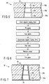
The spacer assembly is manufactured according to
the processes shown in FIG. 6. As shown in FIG. 7 that
representatively illustrates the first die 32, varnish
or some other parting agent that consists mainly of an
organic component and is dissolved in an organic
solvent is applied to and dried on the respective
surfaces of the first and second dies 32 and 33,
thereby forming organic coating films 50. The organic
coating films 50 are spread by spray coating, dipping,
etc., and are formed having a thickness of 50 µm each
after they are dried. The heat decomposition
temperature (first temperature) of the organic coating
films 50 is about 280°C. Organic components that can
be used for the parting agent include acrylic resins,
epoxy resins, urethane resins, mixtures of these
resins, etc.
The organic coating films 50 should only be
located at least on the respective surfaces of the
through holes 34 of the first and second dies 32 and
33, and they need not always be formed on the
respective contact surfaces on the grid and their
opposite surfaces.
Subsequently, the first die 32 is brought
intimately into contact with the first surface 24a of
the grid 24 so that the large-diameter side of each
through hole 34 is situated on the side of the grid,
and is positioned so that each through hole 34 is
aligned with its corresponding spacer aperture 28 of
the grid, as shown in FIG. 8A. Likewise, the second
die 33 is brought intimately into contact with the
second surface 24b of the grid so that the large-diameter
side of each through hole 34 is situated on
the side of the grid 24, and is positioned so that each
through hole 34 is aligned with its corresponding
spacer aperture 28 of the grid. The first die 32, grid
24, and second die 33 are fixed to one another by means
of a clamper (not shown) or the like.
Then, a pasty spacer forming material 40 is
supplied from, for example, the outer surface side of
the first die 32 by means of a squeegee 36, whereupon
the through holes 34 of the first die 32, the spacer
apertures 28 of the grid 24, and the through holes 34
of the second die 33 are filled with the spacer forming
material, as shown in FIG. 8B. An extra portion of
the spacer forming material 40 that is projected onto
the outer surface side of the second die 33 is scraped
off by means of a squeegee 38.
Glass paste that contains, for example, an
ultraviolet-curing binder (organic component) and a
glass filler is used as the spacer forming material 40.
The heat decomposition temperature (second temperature)
of the binder is ranges from about 350°C to 450°C, that
is, the heat decomposition temperature (first
temperature) of the organic coating films 50 is set to
be lower than the second temperature.
Subsequently, ultraviolet rays (UV) are applied as
radiation to the charged spacer forming material 40
from the respective outer surface sides of the first
and second dies 32 and 33, as shown in FIG. 8C, whereby
the spacer forming material is UV-cured.
After the first and second dies 32 and 33 that are
intimately in contact with the grid 24, as shown in
FIG. 9A, are located in a heating oven, moreover, they
are heated at the first temperature of about 280°C for
30 minutes or thereabout. Thereupon, the organic
coating films 50 on the respective surfaces of the
first and second dies 32 and 33 are removed by heat
decomposition or combustion. Thus, gaps corresponding
to the thickness of the organic coating film are
defined between the spacer forming material 40 and the
respective inner surfaces of the through holes 34 of
the first and second dies 32 and 33, so that the first
and second dies can be easily parted from each other.
After the first and second dies 32 and 33 and the
grid 24 are cooled to a given temperature, thereafter,
the first and second dies 32 and 33 are separated from
the grid 24, as shown in FIG. 9B.
Then, the grid 24 and the UV-cured spacer forming
material 40 are heated at the second temperature of
about 350°C to 450°C for 60 minutes or thereabout,
whereupon a binder removing process is accomplished
such that the binder in the spacer forming material 40
is evaporated. Thereafter, the spacer forming material
40 is subjected to regular firing in the heating oven
at a third temperature of about 500°C to 550°C for 30 to
60 minutes. Thereupon, the first and second spacers
30a and 30b that are integral with the grid 24 are
formed. Thus, the spacer assembly 22 in which the grid
24 has the numerous first and second spacers 30a and
30b built-in is completed.
In manufacturing the SED with use of the spacer
assembly 22 manufactured in this manner, the rear plate
10, which is provided with the electron emitting
elements 18 and to which the sidewall 14 is jointed,
and the faceplate 12, which is provided with the
phosphor screen 16 and the metal back 17, are prepared
in advance. The rear plate 10 and the faceplate 12 are
located in a vacuum chamber with the spacer assembly 22
positioned on the rear plate. The faceplate 12 is
jointed to the rear plate 10 by means of the sidewall
14 with the vacuum chamber evacuated. By doing this,
the SED that is provided with the spacer assembly 22 is
manufactured.
According to the method of manufacturing the
spacer assembly constructed in this manner, a plurality
of spacers can be set at a time in given positions on
the grid 24 by curing the spacer forming material 40
that is located on the grid by means of the first and
second dies 32 and 33. Thus, the spacer assembly
provided with a plurality of fine spacers and the SED
can be easily obtained at lower manufacturing cost and
with improved manufacturing efficiency.
After the spacer forming material 40 is cured,
moreover, the first and second dies 32 and 33 are
heated to pyrolize the organic coating films 50 of the
parting agent. Thereupon, the gaps are formed between
the cured spacer forming material and the through holes
of the dies, so that the dies can be easily parted from
each other. After the dies are parted, the binder
removing process and firing are carried out with the
cured spacer forming material 40 exposed. By doing
this, the spacer forming material can be heated and
fired uniformly and efficiently. In consequence, the
spacers with uniform the shape, strength, etc. can be
obtained.
Further, the first and second dies 32 and 33 are
parted from each other when the spacer forming material
40 is subjected to the binder removing and firing.
Therefore, the first and second dies should only be
formed of a material that can stand the first
temperature, so that the heat resistance of the dies
can be lowered. Thus, the molding dies can be
repeatedly used with less oxidation and deformation, so
that the cost of the molding dies can be reduced
considerably.
According to the manufacturing method for the
spacer assembly described above, the diameter of
the spacers 30a and 30b can be easily adjusted by
regulating the thickness of the organic coating
films 50. Thus, the diameter of the spacers 30a and
30b can be reduced, for example, by regulating the
thickness of the organic coating films 50, so that the
resulting spacer assembly 22 can have the spacers with
a high aspect ratio.
According to the present embodiment, on the other
hand, each die is formed by laminating a plurality of
thin metal sheets, having through holes each, to one
another. Usually, it is very hard to form fine through
holes of hundreds of micrometers corresponding to the
diameter for spacer formation in a metal sheet with
a thickness of about 1 mm or more. In contrast with
this, fine through holes can be formed relatively
easily in a thin metal sheet with a thickness of about
0.1 to 0.3 mm by etching or laser working. As in
the present embodiment, therefore, a die having through
holes with a desired height can be easily obtained by
laminating a plurality of thin metal sheets with the
through holes to one another and joining them by
thermocompression bonding.
In the die described above, moreover, the through
holes in each thin metal sheet are in the form of
a truncated cone each, and their diameter varies
according to the thin metal sheet. Thus, the die
having the desired through holes can be obtained by
securely internally connecting the through holes of
a plurality of thin metal sheets if the thin metal
sheets are dislocated to some degree as they are
laminated to one another.
The following is a description of an SED that is
provided with a spacer assembly according to a second
embodiment of this invention and a manufacturing method
therefor.
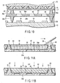
According to the second embodiment, as shown in
FIG. 10, a grid 24 of a spacer assembly 22 has no
spacer apertures, and first and second spacers 30a and
30b are formed independently of one another and
integrally with the grid 24.
Thus, a plurality of first spacers 30a are set up
between beam apertures 26 on a first surface 24a of the
grid 24, and engage the inner surface of a faceplate 12
through a metal back 17 and a black colored layer of
a phosphor screen 16. Further, a plurality of second
spacers 30b are set up between the beam apertures 26 on
a second surface 24b of the grid 24, abut against the
inner surface of a rear plate 10, and are aligned with
the first spacers 30a, individually. The SED shares
other configurations with the SED according to the
first embodiment. Therefore, like reference numerals
are used to designate like portions, and a detailed
description of those portions is omitted.
In manufacturing the spacer assembly 22 having the
construction described above, the first die 32 having
the organic coating film 50 on its surface is first
brought intimately into contact with the first surface
24a of the grid 24 so that the large-diameter side of
each through hole 34 is situated on the side of the
grid, and is positioned so that each through hole is
situated between the beam apertures 26 of the grid, as
shown in FIG. 11A. Subsequently, the pasty spacer
forming material 40 is supplied from the outer surface
side of the first die 32 by means of the squeegee 36,
whereupon the through holes 34 of the first die 32 are
filled with the spacer forming material. The organic
coating film 50, spacer forming material 40, and first
die 32 used are identical with the ones according to
the foregoing embodiment.
Then, ultraviolet rays (UV) are applied to the
spacer forming material 40 that fills the through holes
34 from the outer surface side of the first die 32, as
shown in FIG. 11B, whereby the spacer forming material
is UV-cured.
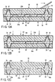
As shown in FIG. 12A, thereafter, the grid 24 and
the first die 32 are kept intimately in contact with
each other as the second die 33, having the organic
coating film 50 formed on its surface, is brought
intimately into contact with the second surface 24b of
the grid 24 so that the large-diameter side of each
through hole 34 is situated on the side of the grid 24,
and is positioned so that each through hole is situated
between the beam apertures 26 of the grid. The first
die 32, grid 24, and second die 33 are fixed to one
another by means of a clamper (not shown) or the like.
Subsequently, the pasty spacer forming material 40
is supplied from the outer surface side of the second
die 33 by the squeegee 36, whereupon the through holes
34 of the second die 33 are filled with the spacer
forming material. The second die 33 used is identical
with the one according to the foregoing embodiment.
Thereafter, ultraviolet rays are applied to the
spacer forming material 40 that fills the through holes
34 from the outer surface side of the second die 33,
whereby the spacer forming material is UV-cured.
After the first and second dies 32 and 33 that are
intimately in contact with the grid 24, as shown in
FIG. 12C, are then located in the heating oven, they
are heated at the first temperature of about 280°C for
30 minutes or thereabout. Thereupon, the organic
coating films 50 on the respective surfaces of the
first and second dies 32 and 33 are removed by heat
decomposition. Thus, gaps corresponding to the
thickness of the organic coating films 50 are formed
between the spacer forming material 40 and the
respective inner surfaces of the through holes 34 of
the first and second dies 32 and 33, so that the first
and second dies can be easily parted from each other.
After the first and second dies 32 and 33 and
the grid 24 are cooled to the given temperature,
thereafter, the first and second dies 32 and 33 are
separated from the grid 24.
Then, the grid 24 and the UV-cured spacer forming
material 40 are heated at the second temperature of
about 350°C to 450°C for 60 minutes or thereabout,
whereupon a binder removing process is accomplished
such that the binder in the spacer forming material 40
is evaporated. Thereafter, the spacer forming material
40 is subjected to regular firing in the heating oven
at the third temperature of about 500°C to 550°C for 30
to 60 minutes. Thereupon, the spacer assembly 22
having the grid 24 and the first and second spacers 30a
and 30b integral with it is completed.
The SED that is provided with the spacer assembly
22 constructed in this manner is manufactured according
to the same processes of the foregoing embodiment.
The second embodiment arranged in this manner can
provide the same functions and effects of the foregoing
embodiment.
In the first and second embodiments described
above, the spacer assembly is constructed so that the
first and second spacers are arranged individually on
the opposite surfaces of the grid 24 in an integral
manner. Alternatively, however, the first or second
spacer may be formed integrally on only one surface of
the grid, and the other spacer, first or second, on the
rear plate or the faceplate.
Further, this present invention is not limited to
the embodiments described above, and that various
changes and modifications may be effected therein by
one skilled in the art without departing from the scope
or spirit of the invention. For example, the spacer
forming material is not limited to the aforementioned
glass paste, and may be suitably selected as required.
Further, the diameter and height of the spacers and the
dimensions, material, etc. of the other components may
be suitably selected as required. Furthermore, the
shape of each spacer is not limited to the shape of
a stepped truncated cone, and may alternatively be the
shape of a truncated cone without steps or any other
shape. The parting agent may be a material that
consists mainly of a binder or organic component
contained by the spacer forming material and is
pyrolized at a lower temperature than the organic
component is, and can be selected suitably.
In the foregoing embodiments, the die that is
formed by laminating a plurality of metal sheets to one
another is used as the molding die. The molding die is
not limited to this, however, and may be changed as
required.
Further, the ultraviolet-curing binder for use as
the spacer forming material may be replaced with
a material that contains a thermosetting binder or
ultraviolet-curing/thermosetting binder (organic
component). After some of the spacer forming material
is cured by heating at a given temperature or with
ultraviolet rays, in this case, the remainder is cured
by heating at the given temperature. The thermal
curing temperature for the spacer forming material is
adjusted to a temperature lower than the heat
decomposition temperature (first temperature) of the
organic coating film that is formed of the parting
agent.
According to the manufacturing method of the
spacer assembly of this invention, the spacers may be
reduced in diameter by etching after the spacer
assembly is formed according to foregoing embodiments.
In the foregoing embodiments, moreover, the
through holes of the dies filled with the spacer
forming material after the dies are brought intimately
into contact with the grid or glass substrate.
Alternatively, the dies may be brought intimately into
contact with the grid or glass substrate after the
through holes of the dies are filled with the spacer
forming material in advance.
Furthermore, this invention is not limited to the
SED, and is applicable to various display devices, such
as FEDs, PDPs, etc., only if they are flat display
devices that are provided with spacers. This invention
is not limited to the spacer assembly with the grid,
and is also applicable to a method of manufacturing
a spacer assembly that includes a metallic or glass
substrate with no beam passage apertures, and
a plurality of spacers.
According to this invention, as described in
detail herein, there may be provided a method of
manufacturing a spacer assembly, capable of easily
manufacturing the spacer assembly of a flat display
device.
Claims (12)
- A method of manufacturing a spacer assembly, which has a substrate and a plurality of columnar spacers provided on the substrate and is used in a flat display device, comprising:preparing the substrate and a molding die having a plurality of through holes;forming an organic coating film by applying a parting agent at least to the respective inner surfaces of the through holes of the molding die, the parting agent containing an organic component which is dissipated by being decomposed or burned by heating at a given temperature;locating the molding die on the surface of the substrate so as to be intimately in contact therewith and then filling a spacer forming material into the through holes of the molding die;curing the filled spacer forming material and then heating the substrate and the molding die at a first temperature to decompose or burn at least the organic coating film on the respective inner surfaces of the through holes of the molding die, thereby removing the organic coating film;parting the molding die from the substrate after the organic coating film is removed;heating the spacer forming material at a second temperature higher than the first temperature, thereby removing a binder from the spacer forming material, after the molding die is parted; andfiring the spacer forming material at a third temperature higher than the first and second temperatures, thereby forming the spacers integrally on the substrate, after the binder removing process.
- A method of manufacturing a spacer assembly according to claim 1, wherein the spacer forming material used is a spacer forming material consisting mainly of a glass filler and an ultraviolet-curing, thermosetting, or ultraviolet-curing/thermosetting organic component such that the substrate and the molding die are heated at the first temperature to remove at least the organic coating film on the respective inner surfaces of the through holes of the molding die after the spacer forming material is cured by being irradiated with ultraviolet rays, after the spacer forming material is cured at a temperature lower than the first temperature, or after at least some of the spacer forming material is cured by being irradiated with ultraviolet rays with the remainder cured thereafter at a temperature lower than the first temperature.
- A method of manufacturing a spacer assembly according to claim 1, wherein the parting agent used is a parting agent consisting mainly of an organic component which is decomposed or burned at a lower temperature than the organic component of the cured spacer forming material is.
- A method of manufacturing a spacer assembly according to claim 1, wherein the diameter of each spacer is adjusted by regulating the thickness of the organic coating film.
- A method of manufacturing a spacer assembly according to claim 1, wherein the substrate used is a metallic substrate coated with an oxide film.
- A method of manufacturing a spacer assembly, which has a plate-shaped grid having a number of beam passage apertures and a plurality of columnar spacers provided integrally on the grid and is used in a flat display device, comprising:preparing the plate-shaped grid having first and second surfaces and a plurality of spacer apertures situated individually between the beam passage apertures;preparing first and second plate-shaped molding dies having a plurality of through holes each;forming organic coating films individually by applying a parting agent at least to the respective inner surfaces of the through holes of the first and second molding dies, the parting agent containing an organic component which is dissipated by being decomposed or burned by heating at a given temperature;locating the first and second molding dies on the first and second surfaces, respectively, of the grid so as to be intimately in contact therewith and so that the spacer apertures of the grid and the through holes of the first and second molding dies are in alignment with one another and then filling the spacer forming material into the through holes of the first and second molding dies and the spacer apertures;curing the filled spacer forming material and then heating the grid and the first and second molding dies at a first temperature to decompose or burn at least the organic coating films on the respective inner surfaces of the through holes of the first and second molding dies, thereby dissipating the organic coating films, and parting the first and second molding dies from the grid thereafter;heating the spacer forming material at a second temperature higher than the first temperature, thereby removing a binder from the spacer forming material, after the first and second molding dies are parted; andfiring the spacer forming material at a third temperature higher than the first and second temperatures, thereby forming the spacers integrally on the first and second surfaces of the grid, after the binder removing process.
- A method of manufacturing a spacer assembly according to claim 6, wherein the spacer forming material used is a spacer forming material consisting mainly of a glass filler and an ultraviolet-curing, thermosetting, or/and ultraviolet-curing/thermosetting organic component such that the substrate and the molding die are heated at the first temperature to dissipate at least the organic coating films on the respective inner surfaces of the through holes of the molding die after the spacer forming material is cured by being irradiated with ultraviolet rays, after the spacer forming material is cured at a temperature lower than the first temperature, or after at least some of the spacer forming material is cured by being irradiated with ultraviolet rays with the remainder cured thereafter at a temperature lower than the first temperature.
- A method of manufacturing a spacer assembly according to claim 6, wherein the parting agent used is a parting agent consisting mainly of an organic component which is decomposed or burned at a lower temperature than the organic component of the cured spacer forming material is.
- A method of manufacturing a spacer assembly according to claim 6, wherein the diameter of each spacer is adjusted by regulating the thickness of the organic coating films.
- A method of manufacturing a spacer assembly according to claim 6, wherein the grid used is a grid formed of a metal sheet having an oxide film on the surface thereof.
- A method of manufacturing a spacer assembly, which has a plate-shaped grid having a number of beam passage apertures and a plurality of columnar spacers provided on the grid and is used in a flat display device, comprising:preparing the plate-shaped grid having first and second surfaces;preparing first and second plate-shaped molding dies having a plurality of through holes each;forming organic coating films individually by applying a parting agent at least to the respective inner surfaces of the through holes of the first and second molding dies, the parting agent containing an organic component which is dissipated by being decomposed or burned by heating at a given temperature;locating the first molding die on the first surface of the grid so as to be intimately in contact therewith and then filling a spacer forming material into the through holes of the first molding die;curing the spacer forming material filled into the through holes of the first molding die;locating the second molding die on the second surface of the grid so as to be intimately in contact therewith and then filling the spacer forming material into the through holes of the second molding die;curing the spacer forming material filled into the through holes of the second molding die;heating the grid and the first and second molding dies at a first temperature to decompose or burn at least the organic coating films on the respective inner surfaces of the through holes of the first and second molding dies, thereby dissipating the organic coating films, after the spacer forming material is cured and parting the first and second molding dies from the grid thereafter;heating the spacer forming material at a second temperature higher than the first temperature, thereby removing a binder from the spacer forming material, after the first and second molding dies are parted; andfiring the spacer forming material at a third temperature higher than the first and second temperatures, thereby forming the spacers integrally on the first and second surfaces of the grid, after the binder removing process.
- A method of manufacturing a spacer assembly according to claim 11, wherein the grid used is a grid formed of a metal sheet having an oxide film on the surface thereof.
Applications Claiming Priority (3)
| Application Number | Priority Date | Filing Date | Title |
|---|---|---|---|
| JP2001217210A JP2003031125A (en) | 2001-07-17 | 2001-07-17 | Manufacturing method of spacer assembly used for flat panel display |
| JP2001217210 | 2001-07-17 | ||
| PCT/JP2002/007175 WO2003009328A1 (en) | 2001-07-17 | 2002-07-15 | Production method for spacer assembly used in flat display unit |
Publications (2)
| Publication Number | Publication Date |
|---|---|
| EP1416509A1 true EP1416509A1 (en) | 2004-05-06 |
| EP1416509A4 EP1416509A4 (en) | 2008-04-02 |
Family
ID=19051580
Family Applications (1)
| Application Number | Title | Priority Date | Filing Date |
|---|---|---|---|
| EP02746063A Withdrawn EP1416509A4 (en) | 2001-07-17 | 2002-07-15 | Production method for spacer assembly used in flat display unit |
Country Status (5)
| Country | Link |
|---|---|
| US (1) | US7220377B2 (en) |
| EP (1) | EP1416509A4 (en) |
| JP (1) | JP2003031125A (en) |
| TW (1) | TW569261B (en) |
| WO (1) | WO2003009328A1 (en) |
Cited By (1)
| Publication number | Priority date | Publication date | Assignee | Title |
|---|---|---|---|---|
| WO2006113413A3 (en) * | 2005-04-15 | 2007-04-12 | 3M Innovative Properties Co | Method of reusing flexible mold and microstructure precursor composition |
Families Citing this family (2)
| Publication number | Priority date | Publication date | Assignee | Title |
|---|---|---|---|---|
| JP2005100843A (en) * | 2003-09-25 | 2005-04-14 | Toshiba Corp | Image display device and spacer structure manufacturing method |
| JP2005197048A (en) * | 2004-01-06 | 2005-07-21 | Toshiba Corp | Image display device and manufacturing method thereof |
Family Cites Families (11)
| Publication number | Priority date | Publication date | Assignee | Title |
|---|---|---|---|---|
| JP2654570B2 (en) * | 1988-05-26 | 1997-09-17 | キヤノン株式会社 | Flat display device and method of manufacturing the same |
| US5424605A (en) * | 1992-04-10 | 1995-06-13 | Silicon Video Corporation | Self supporting flat video display |
| US5232549A (en) * | 1992-04-14 | 1993-08-03 | Micron Technology, Inc. | Spacers for field emission display fabricated via self-aligned high energy ablation |
| US5540108A (en) * | 1994-02-25 | 1996-07-30 | Advanced Mechanical Technology, Inc. | Multi-axis wheel transducer with angular position detector |
| US6251208B1 (en) * | 1996-10-29 | 2001-06-26 | Toshiba Machine Co., Ltd. | Method for manufacturing a structure with fine ribs |
| JP3564913B2 (en) * | 1997-01-29 | 2004-09-15 | 双葉電子工業株式会社 | Support member for hermetic envelope and hermetic envelope |
| US20020000771A1 (en) * | 1998-08-21 | 2002-01-03 | Shichao Ge | Flat panel display with improved micro-electron lens structure |
| JP2001272927A (en) * | 2000-03-23 | 2001-10-05 | Toshiba Corp | Method for manufacturing spacer assembly of flat display device, method for manufacturing flat display device, and flat display device |
| KR100455681B1 (en) * | 2000-03-23 | 2004-11-06 | 가부시끼가이샤 도시바 | Spacer assembly for flat panel display apparatus, method of manufacturing spacer assembly, method of manufacturing flat panel display apparatus, flat panel display apparatus, and mold used in manufacture of spacer assembly |
| JP2001272926A (en) * | 2000-03-23 | 2001-10-05 | Toshiba Corp | Spacer assembly for flat panel display, flat panel display provided with the same, method for manufacturing spacer assembly, mold used for manufacturing spacer assembly |
| US20050156507A1 (en) * | 2002-09-27 | 2005-07-21 | Shigeo Takenaka | Image display device, method of manufacturing a spacer for use in the image display device, and image display device having spacers manufactured by the method |
-
2001
- 2001-07-17 JP JP2001217210A patent/JP2003031125A/en active Pending
-
2002
- 2002-07-15 EP EP02746063A patent/EP1416509A4/en not_active Withdrawn
- 2002-07-15 WO PCT/JP2002/007175 patent/WO2003009328A1/en not_active Ceased
- 2002-07-16 TW TW091115852A patent/TW569261B/en not_active IP Right Cessation
-
2004
- 2004-01-16 US US10/758,420 patent/US7220377B2/en not_active Expired - Fee Related
Cited By (1)
| Publication number | Priority date | Publication date | Assignee | Title |
|---|---|---|---|---|
| WO2006113413A3 (en) * | 2005-04-15 | 2007-04-12 | 3M Innovative Properties Co | Method of reusing flexible mold and microstructure precursor composition |
Also Published As
| Publication number | Publication date |
|---|---|
| TW569261B (en) | 2004-01-01 |
| WO2003009328A1 (en) | 2003-01-30 |
| US20040222346A1 (en) | 2004-11-11 |
| US7220377B2 (en) | 2007-05-22 |
| JP2003031125A (en) | 2003-01-31 |
| EP1416509A4 (en) | 2008-04-02 |
Similar Documents
| Publication | Publication Date | Title |
|---|---|---|
| KR100455681B1 (en) | Spacer assembly for flat panel display apparatus, method of manufacturing spacer assembly, method of manufacturing flat panel display apparatus, flat panel display apparatus, and mold used in manufacture of spacer assembly | |
| JP2001272926A (en) | Spacer assembly for flat panel display, flat panel display provided with the same, method for manufacturing spacer assembly, mold used for manufacturing spacer assembly | |
| US7220377B2 (en) | Method of manufacturing spacer assembly used in flat display device | |
| JP2001272927A (en) | Method for manufacturing spacer assembly of flat display device, method for manufacturing flat display device, and flat display device | |
| EP1437755A1 (en) | Image display apparatus | |
| EP1705686A1 (en) | Image display device and its manufacturing method | |
| EP1492150A1 (en) | Image display apparatus and its manufacturing method | |
| US20040245914A1 (en) | Image display apparatus | |
| JPWO2003102999A1 (en) | Image display device | |
| JP2003051255A (en) | Method of manufacturing spacer assembly and method of manufacturing image display device provided with this spacer assembly | |
| JP2003031126A (en) | Spacer assembly for image display device and method for manufacturing image display device provided with the same | |
| JP2003123672A (en) | Image display device | |
| WO2005020271A1 (en) | Image display device | |
| JP2004319269A (en) | Image display device having spacer structure, method of manufacturing spacer structure, and mold used for manufacturing spacer structure | |
| WO2006019033A1 (en) | Method for manufacturing image display and image display | |
| JP2004253160A (en) | Image display device | |
| JP2003257343A (en) | Image display device | |
| JP2002373607A (en) | Spacer assembly for flat panel display, flat panel display provided with the same, and method of manufacturing spacer assembly | |
| JP2004349008A (en) | Image display device | |
| JP2004273253A (en) | Image display device and method of manufacturing the same | |
| JP2005100843A (en) | Image display device and spacer structure manufacturing method | |
| JP2004319270A (en) | Mold used for manufacturing image display device and spacer assembly | |
| TW200539221A (en) | Image display device | |
| JP2005141987A (en) | Spacer structure reference mold and method of manufacturing the reference mold | |
| JP2006086032A (en) | Image display device |
Legal Events
| Date | Code | Title | Description |
|---|---|---|---|
| PUAI | Public reference made under article 153(3) epc to a published international application that has entered the european phase |
Free format text: ORIGINAL CODE: 0009012 |
|
| 17P | Request for examination filed |
Effective date: 20040205 |
|
| AK | Designated contracting states |
Kind code of ref document: A1 Designated state(s): DE FR GB IT NL |
|
| STAA | Information on the status of an ep patent application or granted ep patent |
Free format text: STATUS: THE APPLICATION HAS BEEN WITHDRAWN |
|
| 18W | Application withdrawn |
Effective date: 20080219 |
|
| A4 | Supplementary search report drawn up and despatched |
Effective date: 20080304 |