EP1416286A2 - Wheatstone bridge - Google Patents
Wheatstone bridge Download PDFInfo
- Publication number
- EP1416286A2 EP1416286A2 EP03256596A EP03256596A EP1416286A2 EP 1416286 A2 EP1416286 A2 EP 1416286A2 EP 03256596 A EP03256596 A EP 03256596A EP 03256596 A EP03256596 A EP 03256596A EP 1416286 A2 EP1416286 A2 EP 1416286A2
- Authority
- EP
- European Patent Office
- Prior art keywords
- output
- bridge
- amplifier
- half bridge
- input
- Prior art date
- Legal status (The legal status is an assumption and is not a legal conclusion. Google has not performed a legal analysis and makes no representation as to the accuracy of the status listed.)
- Granted
Links
Images

Classifications
-
- G—PHYSICS
- G01—MEASURING; TESTING
- G01R—MEASURING ELECTRIC VARIABLES; MEASURING MAGNETIC VARIABLES
- G01R17/00—Measuring arrangements involving comparison with a reference value, e.g. bridge
- G01R17/10—AC or DC measuring bridges
Definitions
- the invention relates generally to Wheatstone bridge circuits used in sensors for monitoring an applied stimulus such as pressure, force, acceleration and the like in automotive safety critical applications and more particularly to ASICs (application specific integrated circuits) having a simple architecture to enable low cost sensors for such applications.
- ASICs application specific integrated circuits
- a sensor of the type described herein is used, for example, in an automotive application for monitoring an applied stimulus, such as brake fluid pressure, force, acceleration and the like and, as in the case of a pressure sensing application, typically comprise a sense element to provide a Wheatstone bridge signal in response to a target stimulus.
- a pressure sensing sense element can be comprised of four piezoresistors bonded to a diaphragm having appropriate interconnectivity and diaphragm placement.
- the sensor typically includes a sense element, a circuit (e.g., ASIC) which amplifies and compensates that signal which then is typically inputted through a wiring harness or the like into an analog to digital converter of an Electronic Control Unit (ECU), for example, for further processing.
- ASIC Electronic Control Unit
- In-range sensor signals are signals within the normal range of output signals over all application tolerances and stimulus range limits.
- safety critical systems have relied on having two sensors with agreement of the sensor signals providing assurance of the validity of the signals. Although this approach provides suitable assurance of signal validity, it is a costly solution requiring an extra sensor, wire harness and connector.
- Another approach has been to add extensive diagnostic circuits in the sensor's ASIC to provide a higher degree of reliability for in-range sensor outputs compared to a similar single sensor not having such diagnostic circuits.
- This approach provides a cost savings over the two sensor approach, however, this approach requires the use of extensive ASIC die area thereby adversely impacting the sensor's cost, complicates the calibration algorithm and does not guarantee signal validity for signals in the active range for all plausible fault conditions.
- the single output format of such a sensor does not detect relatively high occurrence failure modes which can invalidate in-range output signals.
- such failures could occur due to an electrically damaged output stage or excessive connector resistance developed during long driving periods of an automobile having such a sensor.
- a Wheatstone bridge circuit having applied stimulus sensitive piezoresistive bridge elements comprises independent signal conditioning paths for each half bridge.
- Each half bridge is connected between an independent temperature dependent bridge supply voltage and ground.
- the output of each half bridge is connected to one input of a respective amplifier and a selected proportion of the temperature dependent bridge supply voltage is connected to a second input of the respective amplifier.
- the temperature dependent Wheatstone half bridge supply voltages are also inputted to respective offset and gain compensation control circuits which provide temperature compensation of the transfer function of the amplifiers.
- the outputs of the half bridges are a pair of voltage output signals which are mutually proportional to the supply voltages and stimulus.
- the two half bridge outputs have nominally equal stimulus sensitivities of opposite sign.
- the output of the first amplifier connected to the first half bridge is connected to one of two inputs of a third amplifier with the other input of the third amplifier receiving the output of the second amplifier connected to the output of the second half bridge.
- the output of the second amplifier is also connected to the single input of a fourth amplifier so that the output of the third amplifier provides a signal proportional to the Wheatstone bridge differential output voltage and the output of the fourth amplifier provides a signal proportional to the Wheatstone half bridge output voltage.
- each half bridge is connected to the single input of an amplifier having a fixed functional relationship to provide two output signals, each proportional to a respective Wheatstone half bridge output voltage.
- the temperature dependent voltage signal and the signal proportional to the Wheatstone half bridge output voltage are multiplexed to the single input of an output amplifier under the control of a state machine, or the like, to provide a temperature dependent signal on an output node of the ASIC for a selected time period followed by the signal proportional to the Wheatstone half bridge output on the same output node on a continuous basis after the expiry of the time period.
- the above embodiments enable detection of plausible sensor or sensor interconnectivity flaws from the sensor's sense element to the ECU (electronic control unit) input signal measurement circuit in a robust yet simple manner enabling the provision of an improved low cost sensor.
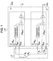
- a full Wheatstone piezoresistive bridge 12 of such a sense element comprises piezoresistors R1 and R2 of one half bridge and piezoresistors R3 and R4 of another half bridge connected separately to five distinct nodes of an integrated circuit (IC) 14.
- Resistors R1 and R2 are connected to the integrated circuit ground GND and supplied by a half bridge voltage supply VHB1 through a series resistance RS1.
- the output of the half bridge composed of R1 and R2 serves as an input to the integrated circuit VINP node.
- Half bridge voltage supply VHB1 preferably is made to be dependent on temperature, specifically the temperature of half bridge R1, R2 by selecting the temperature coefficient of resistance of resistor RS1 to be roughly equal to zero, or at least to be insignificant when compared to the temperature coefficient of resistance of the sum of the resistances of resistors R1, R2.
- the temperature dependence of the voltage signal VHB1 can serve as an input to IC 14 to provide an indication of the half bridge piezoresistor temperature.
- the signal VHB1 serves as an input to compensation control circuit 1 to provide temperature dependent compensation of the transfer function of amplifier U1.
- Amplifier U1 has inputs VINP and ⁇ VHB1. Alpha is a proportionality constant roughly equal to 0.5.
- the output of amplifier U1 is a signal that is generally independent of temperature due to the corrections of compensation control circuit 1 for a fixed input stimulus, e.g., pressure, force and the like.
- the output signal of U1 is generally linear with applied stimulus assuming a linear variation of input signal VINP with stimulus.
- the second bridge half comprising resistors R3 and R4 are connected to IC ground GND and supplied by a half bridge voltage supply VHB2 through a series resistor RS2.
- the output of the half bridge composed of R3 and R4 serves as an input to the IC VINM node.
- the half bridge voltage supply VHB2 preferably is made to be dependent on temperature by selecting the temperature coefficient of resistance of resistor RS2 to be roughly equal to zero, or at least to be insignificant, compared to the temperature coefficient of resistance of the sum of the resistances of resistors R3, R4.
- the signal VHB2 serves as an input to compensation control circuit 2 providing temperature dependent compensation of the transfer function of amplifier U2 having inputs VINM and ⁇ VHB2.
- Beta is a proportionality constant also roughly equal to 0.5.
- the output of amplifier U2 is a signal proportional to applied stimulus generally independent of temperature due to the corrections of compensation control circuit 2 roughly equal to and of opposite slope of the output of amplifier U1.
- the output of amplifier U2 is connected both to amplifier U5 having a fixed functional relation providing drive capability and additional gain to achieve the desired transfer function between stimulus and output voltage signal and to one of two inputs of amplifier U4 whose other input is connected to the output of amplifier U1 of the first half bridge.
- Amplifier U4 has a voltage gain roughly half as large as amplifier U5.
- Output signal P2 of amplifier U5 is proportional to output of amplifier U2, while output signal P1 of amplifier U4 is proportional to the difference between the output of amplifier U2 and the output of amplifier U1, a signal related to the difference between the half bridge output voltages.
- the output signal P1 has a generally equal and opposite slope to that of output signal P2 versus applied stimulus.
- FIG. 2 A second embodiment is shown in Fig. 2.
- the piezoresistive bridge 12, voltage supplies VHB1, VHB2, compensation circuits 1 and 2, amplifiers U1 and U2 and proportionality constants alpha and beta of IC 14' are the same as in the Fig. 1 embodiment and need not be re-described.
- amplifier U6 similar to amplifier U5, has a fixed functional relationship and has a gain corresponding to that of amplifier U5.
- the Fig. 2 embodiment results in a somewhat simpler circuit architecture since an additional small diagnostic circuit (not shown) would normally be included in the Fig. 1 embodiment to provide a detection capability for known sensor failures capable of producing outputs that appear as valid signals at or near the maximum limits of the sensing range.
- the Fig. 1 circuit results in slightly lower noise in output signal P1 due to the lower gain required for amplifier U4
- the circuit of Fig. 2 avoids the Fig.1 gap in diagnostic coverage by generating two signals that are both functionally related to half bridge signals. Further, it has been found that the P2 signal has generally the same accuracy as the P1 signal thereby providing more robust diagnostic coverage.
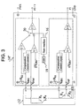
- Fig. 3 shows a modification of the Fig. 2 embodiment.
- the Fig. 3 embodiment provides fault diagnostics in which two signals P1 and P2 of P2/T are compared to determine the validity of the indicated stimulus, e.g., pressure as well as providing a second signal on the P2/T node controllable by a system or a user command.
- the circuit of IC 14" provides an output proportional to the sense element half bridge voltage on the P2/T node for a selected fixed period of time prior to reverting to constant P2 signals on the P2/T node.
- Bridge 12 of Fig. 3 is the same as described above with reference to the Figs. 1 and 2 embodiments.
- IC 14" of the Fig. 3 embodiment adds to the Fig. 2 circuit amplifier U3 having an input connected to half bridge voltage supply VHB2 and whose output is switchable to the input of amplifier U5 under the control of a state machine 16 and oscillator 18 for time multiplexing the P2/T node through switch 20.
- a selected logical progression is followed by the state machine to provide a signal on the P2/T node proportional to sense element temperature at selected times which are not critical to the monitoring of the primary stimulus. That is, this additional operation is based on the particular safety critical monitoring of a primary stimulus, such as information on pressure in an automotive braking application, when such information and the diagnostic coverage can be interrupted for a brief period of time to shut down the power, turn the power back on to yield the temperature signal for a brief period of time before reverting back to the safety critical monitoring operation.
- one suitable time could be when the automobile is stationary, as in start-up, so that monitoring of the hydraulic fluid could be interrupted without a concern of having unsafe conditions during a braking operation.
- Figs. 1-3 typically would be used with a suitable electronic control unit (ECU) of an automobile or the like.
- ECU electronice control unit
- each half of the sensor signal is compensated for offset and span over temperature in compensation circuits 1, 2 yielding a generally constant linear relationship with applied stimulus over a wide temperature range.
- These signals that are supply ratiometric and stimulus ratiometric typically are then converted to a digital signal and mathematically matched to a model in the ECU.
Landscapes
- Physics & Mathematics (AREA)
- General Physics & Mathematics (AREA)
- Measuring Instrument Details And Bridges, And Automatic Balancing Devices (AREA)
- Pressure Sensors (AREA)
- Amplifiers (AREA)
Abstract
Description
- The invention relates generally to Wheatstone bridge circuits used in sensors for monitoring an applied stimulus such as pressure, force, acceleration and the like in automotive safety critical applications and more particularly to ASICs (application specific integrated circuits) having a simple architecture to enable low cost sensors for such applications.
- A sensor of the type described herein is used, for example, in an automotive application for monitoring an applied stimulus, such as brake fluid pressure, force, acceleration and the like and, as in the case of a pressure sensing application, typically comprise a sense element to provide a Wheatstone bridge signal in response to a target stimulus. By way of example, a pressure sensing sense element can be comprised of four piezoresistors bonded to a diaphragm having appropriate interconnectivity and diaphragm placement. The sensor typically includes a sense element, a circuit (e.g., ASIC) which amplifies and compensates that signal which then is typically inputted through a wiring harness or the like into an analog to digital converter of an Electronic Control Unit (ECU), for example, for further processing.
- Many safety critical applications such as automotive electro-hydraulic braking, brake assist, inertial stability systems having braking control and the like, depend on the validity of in-range sensor signals. In-range sensor signals are signals within the normal range of output signals over all application tolerances and stimulus range limits. Conventionally, safety critical systems have relied on having two sensors with agreement of the sensor signals providing assurance of the validity of the signals. Although this approach provides suitable assurance of signal validity, it is a costly solution requiring an extra sensor, wire harness and connector.
- Another approach has been to add extensive diagnostic circuits in the sensor's ASIC to provide a higher degree of reliability for in-range sensor outputs compared to a similar single sensor not having such diagnostic circuits. This approach provides a cost savings over the two sensor approach, however, this approach requires the use of extensive ASIC die area thereby adversely impacting the sensor's cost, complicates the calibration algorithm and does not guarantee signal validity for signals in the active range for all plausible fault conditions. For example, the single output format of such a sensor does not detect relatively high occurrence failure modes which can invalidate in-range output signals. By way of example, such failures could occur due to an electrically damaged output stage or excessive connector resistance developed during long driving periods of an automobile having such a sensor.
- It is an object of the invention to provide a conditioning circuit useful in an ASIC which overcomes the limitations of the prior art mentioned above. Another object is the provision of a simple, low cost conditioning circuit useful with a sensor comprising a Wheatstone bridge having piezoresistive bridge elements which enables improved diagnosis of the sensor signal. Yet another object is the provision of such a circuit which can provide a temperature output, or redundant temperature outputs at selected times such as during a start-up phase of the sensor.
- Briefly in accordance with the invention, a Wheatstone bridge circuit having applied stimulus sensitive piezoresistive bridge elements comprises independent signal conditioning paths for each half bridge. Each half bridge is connected between an independent temperature dependent bridge supply voltage and ground. The output of each half bridge is connected to one input of a respective amplifier and a selected proportion of the temperature dependent bridge supply voltage is connected to a second input of the respective amplifier. The temperature dependent Wheatstone half bridge supply voltages are also inputted to respective offset and gain compensation control circuits which provide temperature compensation of the transfer function of the amplifiers. The outputs of the half bridges are a pair of voltage output signals which are mutually proportional to the supply voltages and stimulus. The two half bridge outputs have nominally equal stimulus sensitivities of opposite sign.
- According to one embodiment, the output of the first amplifier connected to the first half bridge is connected to one of two inputs of a third amplifier with the other input of the third amplifier receiving the output of the second amplifier connected to the output of the second half bridge. The output of the second amplifier is also connected to the single input of a fourth amplifier so that the output of the third amplifier provides a signal proportional to the Wheatstone bridge differential output voltage and the output of the fourth amplifier provides a signal proportional to the Wheatstone half bridge output voltage.
- According to a second embodiment, the output of each half bridge is connected to the single input of an amplifier having a fixed functional relationship to provide two output signals, each proportional to a respective Wheatstone half bridge output voltage.
- According to yet another embodiment, the temperature dependent voltage signal and the signal proportional to the Wheatstone half bridge output voltage are multiplexed to the single input of an output amplifier under the control of a state machine, or the like, to provide a temperature dependent signal on an output node of the ASIC for a selected time period followed by the signal proportional to the Wheatstone half bridge output on the same output node on a continuous basis after the expiry of the time period.
- The above embodiments enable detection of plausible sensor or sensor interconnectivity flaws from the sensor's sense element to the ECU (electronic control unit) input signal measurement circuit in a robust yet simple manner enabling the provision of an improved low cost sensor.
- Other objects, advantages and details of the novel and improved Wheatstone bridge conditioning circuit of the invention appear in the following detailed description of preferred embodiments of the invention, the detailed description referring to the drawings in which:
- Fig. 1 is a schematic diagram of a Wheatstone bridge connected to an ASIC made in accordance with a first preferred embodiment of the invention; and
- Figs. 2 and 3 are schematic diagrams similar to Fig. 1 according to alternative preferred embodiments.
-
- With reference to Fig. 1, a full Wheatstone
piezoresistive bridge 12 of such a sense element comprises piezoresistors R1 and R2 of one half bridge and piezoresistors R3 and R4 of another half bridge connected separately to five distinct nodes of an integrated circuit (IC) 14. Resistors R1 and R2 are connected to the integrated circuit ground GND and supplied by a half bridge voltage supply VHB1 through a series resistance RS1. The output of the half bridge composed of R1 and R2 serves as an input to the integrated circuit VINP node. Half bridge voltage supply VHB1 preferably is made to be dependent on temperature, specifically the temperature of half bridge R1, R2 by selecting the temperature coefficient of resistance of resistor RS1 to be roughly equal to zero, or at least to be insignificant when compared to the temperature coefficient of resistance of the sum of the resistances of resistors R1, R2. With this arrangement, the temperature dependence of the voltage signal VHB1 can serve as an input toIC 14 to provide an indication of the half bridge piezoresistor temperature. The signal VHB1 serves as an input tocompensation control circuit 1 to provide temperature dependent compensation of the transfer function of amplifier U1. Amplifier U1 has inputs VINP and α VHB1. Alpha is a proportionality constant roughly equal to 0.5. The output of amplifier U1 is a signal that is generally independent of temperature due to the corrections ofcompensation control circuit 1 for a fixed input stimulus, e.g., pressure, force and the like. Thus, the output signal of U1 is generally linear with applied stimulus assuming a linear variation of input signal VINP with stimulus. - Similarly, the second bridge half comprising resistors R3 and R4 are connected to IC ground GND and supplied by a half bridge voltage supply VHB2 through a series resistor RS2. The output of the half bridge composed of R3 and R4 serves as an input to the IC VINM node. The half bridge voltage supply VHB2 preferably is made to be dependent on temperature by selecting the temperature coefficient of resistance of resistor RS2 to be roughly equal to zero, or at least to be insignificant, compared to the temperature coefficient of resistance of the sum of the resistances of resistors R3, R4. The signal VHB2 serves as an input to
compensation control circuit 2 providing temperature dependent compensation of the transfer function of amplifier U2 having inputs VINM and β VHB2. Beta is a proportionality constant also roughly equal to 0.5. Thus, the output of amplifier U2 is a signal proportional to applied stimulus generally independent of temperature due to the corrections ofcompensation control circuit 2 roughly equal to and of opposite slope of the output of amplifier U1. - The output of amplifier U2 is connected both to amplifier U5 having a fixed functional relation providing drive capability and additional gain to achieve the desired transfer function between stimulus and output voltage signal and to one of two inputs of amplifier U4 whose other input is connected to the output of amplifier U1 of the first half bridge. Amplifier U4 has a voltage gain roughly half as large as amplifier U5. Output signal P2 of amplifier U5 is proportional to output of amplifier U2, while output signal P1 of amplifier U4 is proportional to the difference between the output of amplifier U2 and the output of amplifier U1, a signal related to the difference between the half bridge output voltages. The output signal P1 has a generally equal and opposite slope to that of output signal P2 versus applied stimulus. This enables the diagnosis by an ECU or the like of a variety of faults which can occur either in the integrated circuit or in either half bridge that would cause a change in one or both of the output signals. Although the described circuit provides voltage output signals, it is within the purview of this invention to provide various other output formats such as electrical current, pulse width modulated voltage, digital voltage or current, etc.
- A second embodiment is shown in Fig. 2. The
piezoresistive bridge 12, voltage supplies VHB1, VHB2,compensation circuits - The Fig. 2 embodiment results in a somewhat simpler circuit architecture since an additional small diagnostic circuit (not shown) would normally be included in the Fig. 1 embodiment to provide a detection capability for known sensor failures capable of producing outputs that appear as valid signals at or near the maximum limits of the sensing range. Although the Fig. 1 circuit results in slightly lower noise in output signal P1 due to the lower gain required for amplifier U4, the circuit of Fig. 2 avoids the Fig.1 gap in diagnostic coverage by generating two signals that are both functionally related to half bridge signals. Further, it has been found that the P2 signal has generally the same accuracy as the P1 signal thereby providing more robust diagnostic coverage.
- Fig. 3 shows a modification of the Fig. 2 embodiment. The Fig. 3 embodiment provides fault diagnostics in which two signals P1 and P2 of P2/T are compared to determine the validity of the indicated stimulus, e.g., pressure as well as providing a second signal on the P2/T node controllable by a system or a user command. The circuit of
IC 14" provides an output proportional to the sense element half bridge voltage on the P2/T node for a selected fixed period of time prior to reverting to constant P2 signals on the P2/T node. Careful control of design and manufacturing parameters such as piezoresistor impurity doping concentration, diaphragm's temperature coefficient of thermal expansion, sensor calibration temperature, etc., can yield a substantially linear half bridge voltage change versus sense element temperature.Bridge 12 of Fig. 3 is the same as described above with reference to the Figs. 1 and 2 embodiments.IC 14" of the Fig. 3 embodiment adds to the Fig. 2 circuit amplifier U3 having an input connected to half bridge voltage supply VHB2 and whose output is switchable to the input of amplifier U5 under the control of astate machine 16 andoscillator 18 for time multiplexing the P2/T node throughswitch 20. Thus a selected logical progression is followed by the state machine to provide a signal on the P2/T node proportional to sense element temperature at selected times which are not critical to the monitoring of the primary stimulus. That is, this additional operation is based on the particular safety critical monitoring of a primary stimulus, such as information on pressure in an automotive braking application, when such information and the diagnostic coverage can be interrupted for a brief period of time to shut down the power, turn the power back on to yield the temperature signal for a brief period of time before reverting back to the safety critical monitoring operation. In the braking example mentioned above, one suitable time could be when the automobile is stationary, as in start-up, so that monitoring of the hydraulic fluid could be interrupted without a concern of having unsafe conditions during a braking operation. - The embodiments of Figs. 1-3 typically would be used with a suitable electronic control unit (ECU) of an automobile or the like. As described above, each half of the sensor signal is compensated for offset and span over temperature in
compensation circuits - It should be understood that although particular embodiments of the invention have been described by way of illustrating the invention, other embodiments and variations of the invention are possible. It is intended that the invention include all modifications and equivalents of the disclosed embodiments falling within the scope of the claims.
Claims (8)
- A Wheatstone bridge conditioning circuit comprising
first and second half bridges and an integrated circuit having an integrated circuit power supply, first and second half bridge power supply nodes connected to at least one power supply for providing first and second half bridge power supplies, first and second integrated circuit half bridge input nodes and at least one ground node,
the first half bridge having first and second stimulus responsive bridge elements serially connected between the first half bridge power supply node and a ground node and having a first half bridge output at the junction between the first and second bridge elements which is connected to the first integrated circuit half bridge input node and the second half bridge having third and fourth stimulus responsive bridge elements serially connected between the second half bridge power supply node and a ground node and having a second half bridge output at the junction between the third and fourth bridge elements which is connected to the second integrated circuit half bridge input node,
first and second offset and gain compensation control circuits,
first and second amplifiers each having two inputs and an output, the integrated circuit first and second half bridge input nodes connected respectively to one input of the first and second amplifiers and the second amplifier inputs of the first and second amplifiers connected to voltage signals proportional to voltages of first and second half bridge power supplies respectively,
the output of the first and second compensation control circuits connected respectively to the first and second amplifiers, the output of the first and second amplifiers each having an output signal proportional to respective first and second Wheatstone half bridge output voltages with each amplifier output signal having offset and gain adjustment to an applied stimulus. - A Wheatstone bridge conditioning circuit according to claim 1 in which the half bridge power supplies are voltage supplies.
- A Wheatstone bridge conditioning circuit according to claim 2 in which the integrated circuit power supply is a substantially fixed voltage supply source and the first and second half bridge power supplies are serially connected through respective first and second resistors to the integrated circuit power supply.
- A Wheatstone bridge conditioning circuit according to claim 2 or claim 3 in which the first and second offset and gain compensation circuits are controlled by the voltages of the first and second half bridge power supplies respectively.
- A Wheatstone bridge conditioning circuit according to any of claims 2 to 4 in which the bridge elements are piezoresistors.
- A Wheatstone bridge conditioning circuit according to claim 5 further comprising third and fourth amplifiers, the third amplifier having first and second inputs and an output and the fourth amplifier having a single input and an output, the output of the second amplifier connected to a first input of the third amplifier and to the input of the fourth amplifier and the output of the first amplifier connected to the second input of the third amplifier, the outputs of the third amplifier providing a signal proportional to the Wheatstone bridge differential output voltage and the output of the fourth amplifier providing a signal proportional to the Wheatstone half bridge output voltages, each output signal having offset and gain adjustment to an applied stimulus.
- A Wheatstone bridge conditioning circuit according to claim 5 further comprising third and fourth amplifiers each having a single input and an output, the outputs of the first and second amplifiers respectively connected to the inputs of the third and fourth amplifiers providing output signals proportional to each respective Wheatstone half bridge output voltage, each output signal having offset and gain adjustment to an applied stimulus.
- A Wheatstone bridge conditioning circuit according to claim 5 further comprising third, fourth and fifth amplifiers, the third, fourth and fifth amplifiers having a single input and an output, the output of the first amplifier connected to the input of the third amplifier,
a multiplexing switch and a state machine, the multiplexing switch having an output connected to the input of the fourth amplifier and an input movable between the outputs of the second and fifth amplifiers under the control of the state machine, the input of the fifth amplifier connected to a temperature dependent half bridge voltage supply signal in which the output of the fourth amplifier provides an output signal proportional to the temperature dependent voltage supply for a selected time following the application of power to the conditioning circuit followed by a continuous output signal proportional to at least one Wheatstone half bridge output voltage.
Applications Claiming Priority (2)
| Application Number | Priority Date | Filing Date | Title |
|---|---|---|---|
| US277797 | 1988-11-30 | ||
| US10/277,797 US6765391B2 (en) | 2002-10-22 | 2002-10-22 | Low cost asic architecture for safety critical applications monitoring an applied stimulus |
Publications (3)
| Publication Number | Publication Date |
|---|---|
| EP1416286A2 true EP1416286A2 (en) | 2004-05-06 |
| EP1416286A3 EP1416286A3 (en) | 2007-11-14 |
| EP1416286B1 EP1416286B1 (en) | 2009-09-23 |
Family
ID=32093358
Family Applications (1)
| Application Number | Title | Priority Date | Filing Date |
|---|---|---|---|
| EP03256596A Expired - Lifetime EP1416286B1 (en) | 2002-10-22 | 2003-10-20 | Wheatstone bridge |
Country Status (4)
| Country | Link |
|---|---|
| US (1) | US6765391B2 (en) |
| EP (1) | EP1416286B1 (en) |
| JP (1) | JP4514432B2 (en) |
| DE (1) | DE60329360D1 (en) |
Families Citing this family (10)
| Publication number | Priority date | Publication date | Assignee | Title |
|---|---|---|---|---|
| US7031863B2 (en) * | 2003-12-22 | 2006-04-18 | Texas Instruments Incorporated | Variable condition responsive sense system and method |
| JP5156671B2 (en) * | 2009-02-27 | 2013-03-06 | 株式会社日立製作所 | Magnetic field detection device and measurement device |
| DE102009028938A1 (en) * | 2009-08-27 | 2011-03-03 | Endress + Hauser Gmbh + Co. Kg | Field device for determining or monitoring a physical or chemical variable |
| JP5669551B2 (en) * | 2010-12-14 | 2015-02-12 | 大和製衡株式会社 | Load cell failure diagnosis device |
| JP5679837B2 (en) * | 2011-01-27 | 2015-03-04 | 大和製衡株式会社 | Weighing device |
| JP5679862B2 (en) * | 2011-02-24 | 2015-03-04 | 大和製衡株式会社 | Hopper type weighing device |
| WO2014006442A1 (en) | 2012-07-02 | 2014-01-09 | Freescale Semiconductor, Inc. | Integrated circuit device, safety circuit, safety-critical system and method of manufacturing an integrated circuit device |
| EP3598148B1 (en) | 2018-07-16 | 2021-03-17 | Melexis Technologies NV | Half-bridge differential sensor |
| EP3647737B1 (en) | 2018-11-05 | 2022-08-03 | Melexis Technologies NV | Sensor interface circuit |
| DE102018128399A1 (en) * | 2018-11-13 | 2020-05-14 | Thyssenkrupp Ag | Steering column for a steering system of a motor vehicle with a control unit for two adjustment drives |
Citations (3)
| Publication number | Priority date | Publication date | Assignee | Title |
|---|---|---|---|---|
| EP0592205A1 (en) | 1992-10-07 | 1994-04-13 | Nec Corporation | Semiconductor sensor with fault detecting circuit |
| US5777235A (en) | 1994-05-17 | 1998-07-07 | Altwein; Michael | Strain gage measuring arrangement, use of same, and modulation amplifier for such measuring arrangements |
| JP2001091387A (en) | 1999-09-27 | 2001-04-06 | Matsushita Electric Works Ltd | Pressure sensor temperature compensation circuit |
Family Cites Families (6)
| Publication number | Priority date | Publication date | Assignee | Title |
|---|---|---|---|---|
| JPS5255568A (en) * | 1975-10-30 | 1977-05-07 | Nippon Denso Co Ltd | Physical quantity detecting apparatus |
| JPH0777266B2 (en) * | 1988-12-28 | 1995-08-16 | 株式会社豊田中央研究所 | Semiconductor strain detector |
| US5770802A (en) * | 1997-04-16 | 1998-06-23 | Texas Instruments Incorporated | Sensor with improved capacitive to voltage converter integrated circuit |
| DE19852502A1 (en) * | 1998-11-13 | 2000-05-18 | Philips Corp Intellectual Pty | Method for the offset calibration of a magnetoresistive angle sensor |
| US6433554B1 (en) * | 1999-12-20 | 2002-08-13 | Texas Instruments Incorporated | Method and apparatus for in-range fault detection of condition responsive sensor |
| US6549138B2 (en) * | 2000-09-20 | 2003-04-15 | Texas Instruments Incorporated | Method and apparatus for providing detection of excessive negative offset of a sensor |
-
2002
- 2002-10-22 US US10/277,797 patent/US6765391B2/en not_active Expired - Lifetime
-
2003
- 2003-10-20 EP EP03256596A patent/EP1416286B1/en not_active Expired - Lifetime
- 2003-10-20 DE DE60329360T patent/DE60329360D1/en not_active Expired - Lifetime
- 2003-10-21 JP JP2003360315A patent/JP4514432B2/en not_active Expired - Fee Related
Patent Citations (3)
| Publication number | Priority date | Publication date | Assignee | Title |
|---|---|---|---|---|
| EP0592205A1 (en) | 1992-10-07 | 1994-04-13 | Nec Corporation | Semiconductor sensor with fault detecting circuit |
| US5777235A (en) | 1994-05-17 | 1998-07-07 | Altwein; Michael | Strain gage measuring arrangement, use of same, and modulation amplifier for such measuring arrangements |
| JP2001091387A (en) | 1999-09-27 | 2001-04-06 | Matsushita Electric Works Ltd | Pressure sensor temperature compensation circuit |
Also Published As
| Publication number | Publication date |
|---|---|
| JP4514432B2 (en) | 2010-07-28 |
| US6765391B2 (en) | 2004-07-20 |
| DE60329360D1 (en) | 2009-11-05 |
| JP2004144751A (en) | 2004-05-20 |
| US20040075447A1 (en) | 2004-04-22 |
| EP1416286A3 (en) | 2007-11-14 |
| EP1416286B1 (en) | 2009-09-23 |
Similar Documents
| Publication | Publication Date | Title |
|---|---|---|
| US6040779A (en) | Method and circuit for monitoring the functioning of a sensor bridge | |
| US6843537B2 (en) | High reliability pressure sensor | |
| CA2145698C (en) | Electronic circuit for a transducer | |
| US20020067255A1 (en) | Physical-quantity detection sensor | |
| US5789925A (en) | Sensor system having abnormality detecting circuit for detecting abnormality of sensor system from outputs of signal processing circuits | |
| US6765391B2 (en) | Low cost asic architecture for safety critical applications monitoring an applied stimulus | |
| US5631602A (en) | Wheatstone bridge amplifier circuit with integrated diagnostic testing | |
| JP3564796B2 (en) | Sensor device and method of adjusting sensor device | |
| JPH04185552A (en) | Failure detection device of passenger protective device | |
| JP4438222B2 (en) | Physical quantity detection device | |
| JP3274034B2 (en) | Semiconductor acceleration detector | |
| JP4549176B2 (en) | Detection system and method responsive to variable conditions | |
| US6011422A (en) | Integrated differential voltage amplifier with programmable gain and input offset voltage | |
| JP4487416B2 (en) | Physical quantity detection device | |
| JPH0753499B2 (en) | Failure detection device for airbag device | |
| WO1991007713A1 (en) | Transducer power supply | |
| EP0749001B1 (en) | Offset cancel circuit and offset cancel method using the same | |
| JP4345207B2 (en) | Mechanical quantity detection sensor | |
| EP3598148B1 (en) | Half-bridge differential sensor | |
| JP2001194256A (en) | Sensor device | |
| JP4352555B2 (en) | Pressure sensor | |
| JP2002084151A (en) | Physical quantity detector | |
| JPH04307331A (en) | Complex sensor | |
| JP2002013995A (en) | Dynamic quantity detecting sensor | |
| GB2238132A (en) | Transducer power supply |
Legal Events
| Date | Code | Title | Description |
|---|---|---|---|
| PUAI | Public reference made under article 153(3) epc to a published international application that has entered the european phase |
Free format text: ORIGINAL CODE: 0009012 |
|
| AK | Designated contracting states |
Kind code of ref document: A2 Designated state(s): AT BE BG CH CY CZ DE DK EE ES FI FR GB GR HU IE IT LI LU MC NL PT RO SE SI SK TR |
|
| AX | Request for extension of the european patent |
Extension state: AL LT LV MK |
|
| RAP1 | Party data changed (applicant data changed or rights of an application transferred) |
Owner name: SENSATA TECHNOLOGIES, INC. |
|
| PUAL | Search report despatched |
Free format text: ORIGINAL CODE: 0009013 |
|
| AK | Designated contracting states |
Kind code of ref document: A3 Designated state(s): AT BE BG CH CY CZ DE DK EE ES FI FR GB GR HU IE IT LI LU MC NL PT RO SE SI SK TR |
|
| AX | Request for extension of the european patent |
Extension state: AL LT LV MK |
|
| 17P | Request for examination filed |
Effective date: 20080109 |
|
| 17Q | First examination report despatched |
Effective date: 20080414 |
|
| AKX | Designation fees paid |
Designated state(s): DE FR GB |
|
| GRAP | Despatch of communication of intention to grant a patent |
Free format text: ORIGINAL CODE: EPIDOSNIGR1 |
|
| GRAS | Grant fee paid |
Free format text: ORIGINAL CODE: EPIDOSNIGR3 |
|
| GRAA | (expected) grant |
Free format text: ORIGINAL CODE: 0009210 |
|
| STAA | Information on the status of an ep patent application or granted ep patent |
Free format text: STATUS: THE PATENT HAS BEEN GRANTED |
|
| AK | Designated contracting states |
Kind code of ref document: B1 Designated state(s): DE FR GB |
|
| REG | Reference to a national code |
Ref country code: GB Ref legal event code: FG4D |
|
| REF | Corresponds to: |
Ref document number: 60329360 Country of ref document: DE Date of ref document: 20091105 Kind code of ref document: P |
|
| PLBE | No opposition filed within time limit |
Free format text: ORIGINAL CODE: 0009261 |
|
| STAA | Information on the status of an ep patent application or granted ep patent |
Free format text: STATUS: NO OPPOSITION FILED WITHIN TIME LIMIT |
|
| 26N | No opposition filed |
Effective date: 20100624 |
|
| PGFP | Annual fee paid to national office [announced via postgrant information from national office to epo] |
Ref country code: FR Payment date: 20111005 Year of fee payment: 9 |
|
| REG | Reference to a national code |
Ref country code: FR Ref legal event code: ST Effective date: 20130628 |
|
| PG25 | Lapsed in a contracting state [announced via postgrant information from national office to epo] |
Ref country code: FR Free format text: LAPSE BECAUSE OF NON-PAYMENT OF DUE FEES Effective date: 20121031 |
|
| PGFP | Annual fee paid to national office [announced via postgrant information from national office to epo] |
Ref country code: GB Payment date: 20140925 Year of fee payment: 12 |
|
| PGFP | Annual fee paid to national office [announced via postgrant information from national office to epo] |
Ref country code: DE Payment date: 20141028 Year of fee payment: 12 |
|
| REG | Reference to a national code |
Ref country code: DE Ref legal event code: R119 Ref document number: 60329360 Country of ref document: DE |
|
| GBPC | Gb: european patent ceased through non-payment of renewal fee |
Effective date: 20151020 |
|
| PG25 | Lapsed in a contracting state [announced via postgrant information from national office to epo] |
Ref country code: DE Free format text: LAPSE BECAUSE OF NON-PAYMENT OF DUE FEES Effective date: 20160503 Ref country code: GB Free format text: LAPSE BECAUSE OF NON-PAYMENT OF DUE FEES Effective date: 20151020 |