EP1415338B1 - Dual layer hard mask for edram gate etch process - Google Patents
Dual layer hard mask for edram gate etch process Download PDFInfo
- Publication number
- EP1415338B1 EP1415338B1 EP02764835A EP02764835A EP1415338B1 EP 1415338 B1 EP1415338 B1 EP 1415338B1 EP 02764835 A EP02764835 A EP 02764835A EP 02764835 A EP02764835 A EP 02764835A EP 1415338 B1 EP1415338 B1 EP 1415338B1
- Authority
- EP
- European Patent Office
- Prior art keywords
- region
- hard mask
- mask pattern
- layer
- gate
- Prior art date
- Legal status (The legal status is an assumption and is not a legal conclusion. Google has not performed a legal analysis and makes no representation as to the accuracy of the status listed.)
- Expired - Lifetime
Links
Images




Classifications
-
- H—ELECTRICITY
- H10—SEMICONDUCTOR DEVICES; ELECTRIC SOLID-STATE DEVICES NOT OTHERWISE PROVIDED FOR
- H10B—ELECTRONIC MEMORY DEVICES
- H10B12/00—Dynamic random access memory [DRAM] devices
- H10B12/01—Manufacture or treatment
- H10B12/09—Manufacture or treatment with simultaneous manufacture of the peripheral circuit region and memory cells
-
- H—ELECTRICITY
- H10—SEMICONDUCTOR DEVICES; ELECTRIC SOLID-STATE DEVICES NOT OTHERWISE PROVIDED FOR
- H10D—INORGANIC ELECTRIC SEMICONDUCTOR DEVICES
- H10D84/00—Integrated devices formed in or on semiconductor substrates that comprise only semiconducting layers, e.g. on Si wafers or on GaAs-on-Si wafers
- H10D84/01—Manufacture or treatment
- H10D84/0123—Integrating together multiple components covered by H10D12/00 or H10D30/00, e.g. integrating multiple IGBTs
- H10D84/0126—Integrating together multiple components covered by H10D12/00 or H10D30/00, e.g. integrating multiple IGBTs the components including insulated gates, e.g. IGFETs
- H10D84/0135—Manufacturing their gate conductors
-
- H—ELECTRICITY
- H10—SEMICONDUCTOR DEVICES; ELECTRIC SOLID-STATE DEVICES NOT OTHERWISE PROVIDED FOR
- H10D—INORGANIC ELECTRIC SEMICONDUCTOR DEVICES
- H10D84/00—Integrated devices formed in or on semiconductor substrates that comprise only semiconducting layers, e.g. on Si wafers or on GaAs-on-Si wafers
- H10D84/01—Manufacture or treatment
- H10D84/0123—Integrating together multiple components covered by H10D12/00 or H10D30/00, e.g. integrating multiple IGBTs
- H10D84/0126—Integrating together multiple components covered by H10D12/00 or H10D30/00, e.g. integrating multiple IGBTs the components including insulated gates, e.g. IGFETs
- H10D84/0149—Manufacturing their interconnections or electrodes, e.g. source or drain electrodes
-
- H—ELECTRICITY
- H10—SEMICONDUCTOR DEVICES; ELECTRIC SOLID-STATE DEVICES NOT OTHERWISE PROVIDED FOR
- H10D—INORGANIC ELECTRIC SEMICONDUCTOR DEVICES
- H10D84/00—Integrated devices formed in or on semiconductor substrates that comprise only semiconducting layers, e.g. on Si wafers or on GaAs-on-Si wafers
- H10D84/01—Manufacture or treatment
- H10D84/02—Manufacture or treatment characterised by using material-based technologies
- H10D84/03—Manufacture or treatment characterised by using material-based technologies using Group IV technology, e.g. silicon technology or silicon-carbide [SiC] technology
- H10D84/038—Manufacture or treatment characterised by using material-based technologies using Group IV technology, e.g. silicon technology or silicon-carbide [SiC] technology using silicon technology, e.g. SiGe
-
- H—ELECTRICITY
- H10—SEMICONDUCTOR DEVICES; ELECTRIC SOLID-STATE DEVICES NOT OTHERWISE PROVIDED FOR
- H10P—GENERIC PROCESSES OR APPARATUS FOR THE MANUFACTURE OR TREATMENT OF DEVICES COVERED BY CLASS H10
- H10P50/00—Etching of wafers, substrates or parts of devices
- H10P50/71—Etching of wafers, substrates or parts of devices using masks for conductive or resistive materials
-
- H—ELECTRICITY
- H10—SEMICONDUCTOR DEVICES; ELECTRIC SOLID-STATE DEVICES NOT OTHERWISE PROVIDED FOR
- H10W—GENERIC PACKAGES, INTERCONNECTIONS, CONNECTORS OR OTHER CONSTRUCTIONAL DETAILS OF DEVICES COVERED BY CLASS H10
- H10W20/00—Interconnections in chips, wafers or substrates
- H10W20/01—Manufacture or treatment
- H10W20/031—Manufacture or treatment of conductive parts of the interconnections
- H10W20/069—Manufacture or treatment of conductive parts of the interconnections by forming self-aligned vias or self-aligned contact plugs
-
- H—ELECTRICITY
- H10—SEMICONDUCTOR DEVICES; ELECTRIC SOLID-STATE DEVICES NOT OTHERWISE PROVIDED FOR
- H10B—ELECTRONIC MEMORY DEVICES
- H10B12/00—Dynamic random access memory [DRAM] devices
- H10B12/01—Manufacture or treatment
- H10B12/02—Manufacture or treatment for one transistor one-capacitor [1T-1C] memory cells
- H10B12/05—Making the transistor
Definitions
- This invention relates generally to the fabrication of integrated circuit devices.
- the invention particularly relates to integrating, on a single chip of "embedded Dynamic Access Memory” (eDRAM) products, self-aligned, borderless contacts in DRAM arrays in a first region and bordered contacts in a logic support area in a second region, using a single poly-Si patterning process (lithography and etch) and a single contact definition process.
- eDRAM embedded Dynamic Access Memory
- the invention addresses the problem of fabrication of an integrated circuit chip having two different layout rules on the same chip. In this case, a highly packed layout is used for the gate contacts of the DRAM array region in contrast to a more separated layout for gate contacts in the region containing support logic circuits. Components are concurrently fabricated in both areas, overcoming prior art techniques of having to deal separately with the respective region devices.
- an object of the present invention according to claim 1 to provide a method for generating self-aligned, borderless contacts in DRAM arrays and bordered contacts in a logic support area on eDRAM products using a single contact definition process (lithography and etch).
- a method of fabricating an integrated circuit chip having a first region of a first layout rule and a second region of a second layout rule including: using a first material to establish a first hard mask pattern in only the first region; and, using a second material to establish a second hard mask pattern on top of the first hard mask pattern, the second material further establishing a third hard mask pattern in the second region.
- a method of fabricating eDRAM on an integrated circuit chip including: using a first material to establish a first hard mask pattern only in a first region to contain a DRAM array; and, using a second material to establish a second hard mask pattern on top of the first hard mask pattern, the second material further establishing a third hard mask pattern in a second region.
- a method of fabricating eDRAM on an integrated circuit chip including: initially depositing an oxide layer over the top surface of the chip, using a first material to establish a first hard mask pattern only in a first region of the chip, where the first region is preselected to include a DRAM array; using a second material to establish a second hard mask pattern on top of the first hard mask pattern, where the second material further establishes a third hard mask pattern in a second region of the chip, where the second region is preselected to contain control logic; using an etch process to form gate stacks simultaneously in the first region and the second region; and, forming simultaneously borderless contact studs in the first region and bordered contact studs in the second region.
- a method of fabricating eDRAM on an integrated circuit chip including: using a first material to establish a first hard mask pattern only in a first region of the chip, where the first region is preselected to include a DRAM array; using a second material to establish a second hard mask pattern on top of the first hard mask pattern, where the second material additionally is used to establish a third hard mask pattern in a second region of the chip, where the second region is preselected to include control logic; and forming simultaneously borderless contact studs in the first region and bordered contact studs in the second region.
- a fifth example of the invention described herein is a method of fabricating an integrated circuit chip having a first region having a first set of devices with a first layout rule and a second region having a second set of devices with a second layout rule, the method including: forming a dual hard mask in the first region; and, simultaneously forming the first set of devices and the second set of devices.
- This invention generates self aligned, borderless contacts in DRAM arrays and bordered contacts in logic support area on eDRAM products using a single contact definition process (lithography and etch).
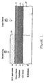
- this figure shows a simplified cross section of a wafer intended to have an eDRAM array in region A and support logic circuitry in region B.
- the wafer includes substrate 10 which has been covered by a gate oxide layer 11 and a polysilicon layer 12.
- This effect is achieved by introducing a thick nitride etch stop layer 13 (approximately 100 nm) which will remain only in the array area A at the hardmask stage, meaning here on top of the polysilicon (poly-Si) layer 12.
- the exact thickness of this nitride layer is not critical and the range of thickness depends upon the characteristics of the etch used in the gate etch step.
- the nitride thickness is predetermined by considering the selectivity of the gate etchant to nitride and the specific geometry of the gates (see Figure 11 for contact hole etch step, wherein the etch for the borderless contact hole 1101 possibly overlaps the gate stack and thereby results in etching away some the silicon nitride barrier for that gate stack).
- Etchants that etch away both the poly-Si layer 12 as well as nitride would require a thicker initial nitride layer 13. Silicon nitride layer 13 would typically be formed using a LPCVD process.
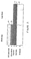
- the nitride layer 13 is first deposited over the entire wafer and then selectively etched in all areas except the array area A by using a standard (blocking) etch mask layer 14, followed by the etching of nitride in areas not covered by the resist mask 14 ( Figure 2). That is to say, since the nitride layer is important only in the region A having the DRAM array, it is removed from the region B having the support logic circuits, using relatively inexpensive Middle Ultra Violet (MUV) photoresist to block the etching of the silicon nitride layer in region A.
- An MUV (Middle Ultra Violet) blocking level mask 14 is deposited using standard photolithographic techniques.
- the nitride is then removed from logic circuit region B using a selective silicon nitride etch.
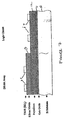
- the remaining MUV resist 14 is stripped (see Figure 3) and a thin TEOS layer 40 is deposited (see Figure 4) over the entire wafer.
- a more expensive Deep Ultra Violet (DUV) masked etch having a shorter wavelength of 193 nm will be used for the hardmask open step to follow. Therefore, a DUV mask will be used for gate patterns in both the DRAM array region A and logic region B, using standard lithographic techniques.
- the litho focus window is found to be large enough in the array area. It should be noted that the step caused by the silicon nitride 14 remaining in the DRAM region potentially causes a focus problem for the subsequent photolithographic steps. However, the litho focus window has been found to be large enough in the array area, meaning that the step-height difference between the logic area and the DRAM area does not cause a focus problem.
- an ARC (Anti-Reflective Coating) layer 50 for reducing surface interference in the subsequent photolithographic steps is first deposited on top of TEOS layer 40, followed by deposition of a DUV Photo Resist layer.
- This DUV Photo Resist layer is then developed using a standard photolithographic process.
- Figure 5 shows the result of this photolithographic development and subsequent etch to leave the DUV photoresist pattern 51. This pattern define the areas to become the gate contacts.
- Figure 6 shows that TEOS caps 60 are formed by the DUV masked etch. These TEOS caps 60 will become the TEOS hard mask stop once the DUV photoresist and ARC layers remnants are stripped (see Figure 7).
- the etch step result of Figure 8 shows that the pattern has been transferred to the silicon nitride layer, which allows the underlying polysilicon layer 12 to be etched to form the gate stacks 90 shown in Figure 9.
- Figure 8 shows the selectively etching off the nitride cap 13 on top of the poly-Si in array region A, using a silicon nitride etch of high selectivity to both oxide and poly so the etch of TEOS and poly-Si is minimized.
- the etch here needs to minimize the loss of cap TEOS in both the logic and DRAM areas and exposed silicon in the logic area so the gate etch in Figure 9 can have a more uniformed poly-silicon layer and adequate TEOS cap layer as a mask.
- the structure shown in Figure 9 following the gate stack 90 etching away unprotected polysilicon 12 provides pre-doped poly-Si gates with a dual-layer hard mask (thin TEOS combined with thick nitride) in the array area A and poly-Si gates with a thin TEOS (tetraethoxysilane) hard mask in the logic support area B.
- a highly selective nitride to oxide and nitride to poly-Si etch process for mask etching results in this simple integration scheme.
- One of the key advantages of this invention is that the gate stacks are simultaneously formed in both the higher density DRAM region and the logic circuit region. The remaining steps merely continue to form the device simultaneously in both regions.
- Figure 10 shows an intermediate step in this construction process.
- the TEOS caps 90 (see Figure 9) have been stripped and spacers 100 formed of silicon nitride have been formed around the gate contacts.
- Spacer formation uses the known technique of depositing and selectively etching a layer of silicon nitride.
- Transistor source/drain diffusion regions 101 are then established, using the gate stack/spacer structures as self-alignment masks for a standard ion implantation process.
- Silicon nitride barrier layer 102 is then deposited, followed by deposition of BPSG layer 103, which serves as a fill-in and leveling layer.
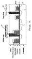
- Figure 11 shows one possible etching technique to form the final contacts with preselected source/drain regions. Standard photolithographic techniques are used to define regions to be etched through the BPSG layer for borderless contact holes 110 in the DRAM region and for bordered contact holes 111 in the logic circuit region. Although Figure 11 shows the BPSG layer etch as involving the entire layer, an alternative would be removal of the top portion of this layer by CMP until the top of the silicon nitride barrier layer of the gate stacks are exposed and then etching the contact holes down to the diffusion regions 101.
- a polysilicon or tungsten layer is deposited and polished back by CMP to be essentially planar with the BPSG layer and provide borderless contact stud 120 and bordered contact stud 121.
- the borderless contact etch can allow contact holes to be either partially landed on or not landed at all on the gate stack. Very tight overlay requirement generally needs high rework rate, if feasible at all, which is an additional cost.
Landscapes
- Engineering & Computer Science (AREA)
- Manufacturing & Machinery (AREA)
- Semiconductor Memories (AREA)
- Internal Circuitry In Semiconductor Integrated Circuit Devices (AREA)
- Metal-Oxide And Bipolar Metal-Oxide Semiconductor Integrated Circuits (AREA)
Description
- This invention relates generally to the fabrication of integrated circuit devices. The invention particularly relates to integrating, on a single chip of "embedded Dynamic Access Memory" (eDRAM) products, self-aligned, borderless contacts in DRAM arrays in a first region and bordered contacts in a logic support area in a second region, using a single poly-Si patterning process (lithography and etch) and a single contact definition process. The invention addresses the problem of fabrication of an integrated circuit chip having two different layout rules on the same chip. In this case, a highly packed layout is used for the gate contacts of the DRAM array region in contrast to a more separated layout for gate contacts in the region containing support logic circuits. Components are concurrently fabricated in both areas, overcoming prior art techniques of having to deal separately with the respective region devices.
- In prior-art document US 2002094637, a method was described of using two separate critical DUV photoresist masks to form the dual gates sequentially with a blocking non-critical MUV photoresist mask for separation. However, this method has a higher manufacturing cost due to the use of two DUV masks. In another prior art re-oxidized polysilicon gate inside the contact holes provides the isolation instead of using thick cap nitride layer. The drawback of this scheme is that it has very narrow process windows and is difficult for manufacturing.
- In the closed packed DRAM array, there is no room for contact borders, so the borderless contacts are preferred which in turn requires the use of a thick nitride cap layer to protect the polysilicon gate when the contact via etch is being made in between the closely packed gate lines. On the other hand, the logic area has no such requirement and the need for a silicidation process precludes the use of thick cap nitride layer. This invention aims to provide a novel scheme to create such a structure having two distinctive layout requirements.
- Reference is likewise made to JP-A-2000243937.
- It is, therefore, an object of the present invention according to claim 1 to provide a method for generating self-aligned, borderless contacts in DRAM arrays and bordered contacts in a logic support area on eDRAM products using a single contact definition process (lithography and etch).
- It is an additional object of the invention to provide a fabrication method for a chip containing regions having different design rule requirements.
- It is an additional object to provide a method that is simpler, less costly, and relaxes the litho overlay requirement for the MOL (middle of the line) process.
- To achieve the above objects and goals, according to a first example of the invention, described herein is a method of fabricating an integrated circuit chip having a first region of a first layout rule and a second region of a second layout rule, including: using a first material to establish a first hard mask pattern in only the first region; and, using a second material to establish a second hard mask pattern on top of the first hard mask pattern, the second material further establishing a third hard mask pattern in the second region.
- According to a second example of the invention, described herein is a method of fabricating eDRAM on an integrated circuit chip, including: using a first material to establish a first hard mask pattern only in a first region to contain a DRAM array; and, using a second material to establish a second hard mask pattern on top of the first hard mask pattern, the second material further establishing a third hard mask pattern in a second region.
- According to a third example of the invention, described herein is a method of fabricating eDRAM on an integrated circuit chip, including: initially depositing an oxide layer over the top surface of the chip, using a first material to establish a first hard mask pattern only in a first region of the chip, where the first region is preselected to include a DRAM array; using a second material to establish a second hard mask pattern on top of the first hard mask pattern, where the second material further establishes a third hard mask pattern in a second region of the chip, where the second region is preselected to contain control logic; using an etch process to form gate stacks simultaneously in the first region and the second region; and, forming simultaneously borderless contact studs in the first region and bordered contact studs in the second region.
- According to a fourth example of the invention, described herein is a method of fabricating eDRAM on an integrated circuit chip, including: using a first material to establish a first hard mask pattern only in a first region of the chip, where the first region is preselected to include a DRAM array; using a second material to establish a second hard mask pattern on top of the first hard mask pattern, where the second material additionally is used to establish a third hard mask pattern in a second region of the chip, where the second region is preselected to include control logic; and forming simultaneously borderless contact studs in the first region and bordered contact studs in the second region.
- According to a fifth example of the invention, described herein is a method of fabricating an integrated circuit chip having a first region having a first set of devices with a first layout rule and a second region having a second set of devices with a second layout rule, the method including: forming a dual hard mask in the first region; and, simultaneously forming the first set of devices and the second set of devices.
- The foregoing and other objects, aspects and advantages will be better understood from the following detailed description of a preferred embodiment of the invention with reference to the drawings, in which:
- Figures 1-11 show the process steps of the invention; and
- Figure 12 shows the final step of a completed eDRAM structure having an array region and logic region formed according to the method of the invention.
- This invention generates self aligned, borderless contacts in DRAM arrays and bordered contacts in logic support area on eDRAM products using a single contact definition process (lithography and etch). Referring now to the drawings, and more particularly to Figure 1, this figure shows a simplified cross section of a wafer intended to have an eDRAM array in region A and support logic circuitry in region B. The wafer includes
substrate 10 which has been covered by agate oxide layer 11 and apolysilicon layer 12. -
Gate oxide layer 11 andpolysilicon layer 12 interplay with the invention since a key aspect of the method is that of allowing regions on the same chip having two different layout styles, where both regions have devices using the oxide layer for transistor gate insulators and the polysilicon layer as gate contacts. This effect is achieved by introducing a thick nitride etch stop layer 13 (approximately 100 nm) which will remain only in the array area A at the hardmask stage, meaning here on top of the polysilicon (poly-Si)layer 12. The exact thickness of this nitride layer is not critical and the range of thickness depends upon the characteristics of the etch used in the gate etch step. The nitride thickness is predetermined by considering the selectivity of the gate etchant to nitride and the specific geometry of the gates (see Figure 11 for contact hole etch step, wherein the etch for the borderless contact hole 1101 possibly overlaps the gate stack and thereby results in etching away some the silicon nitride barrier for that gate stack). Etchants that etch away both the poly-Si layer 12 as well as nitride would require a thickerinitial nitride layer 13.Silicon nitride layer 13 would typically be formed using a LPCVD process. - The
nitride layer 13 is first deposited over the entire wafer and then selectively etched in all areas except the array area A by using a standard (blocking)etch mask layer 14, followed by the etching of nitride in areas not covered by the resist mask 14 (Figure 2). That is to say, since the nitride layer is important only in the region A having the DRAM array, it is removed from the region B having the support logic circuits, using relatively inexpensive Middle Ultra Violet (MUV) photoresist to block the etching of the silicon nitride layer in region A. An MUV (Middle Ultra Violet)blocking level mask 14 is deposited using standard photolithographic techniques. The nitride is then removed from logic circuit region B using a selective silicon nitride etch. Next, theremaining MUV resist 14 is stripped (see Figure 3) and athin TEOS layer 40 is deposited (see Figure 4) over the entire wafer. - In order to get the higher definition of the tightly packed features required in the DRAM array region, a more expensive Deep Ultra Violet (DUV) masked etch having a shorter wavelength of 193 nm will be used for the hardmask open step to follow. Therefore, a DUV mask will be used for gate patterns in both the DRAM array region A and logic region B, using standard lithographic techniques. The litho focus window is found to be large enough in the array area. It should be noted that the step caused by the
silicon nitride 14 remaining in the DRAM region potentially causes a focus problem for the subsequent photolithographic steps. However, the litho focus window has been found to be large enough in the array area, meaning that the step-height difference between the logic area and the DRAM area does not cause a focus problem. - To achieve the etch that will define the gate contacts, an ARC (Anti-Reflective Coating)
layer 50 for reducing surface interference in the subsequent photolithographic steps is first deposited on top ofTEOS layer 40, followed by deposition of a DUV Photo Resist layer. This DUV Photo Resist layer is then developed using a standard photolithographic process. Figure 5 shows the result of this photolithographic development and subsequent etch to leave theDUV photoresist pattern 51. This pattern define the areas to become the gate contacts. - Figure 6 shows that TEOS caps 60 are formed by the DUV masked etch. These TEOS caps 60 will become the TEOS hard mask stop once the DUV photoresist and ARC layers remnants are stripped (see Figure 7). The etch step result of Figure 8 shows that the pattern has been transferred to the silicon nitride layer, which allows the
underlying polysilicon layer 12 to be etched to form thegate stacks 90 shown in Figure 9. Figure 8 shows the selectively etching off thenitride cap 13 on top of the poly-Si in array region A, using a silicon nitride etch of high selectivity to both oxide and poly so the etch of TEOS and poly-Si is minimized. The etch here needs to minimize the loss of cap TEOS in both the logic and DRAM areas and exposed silicon in the logic area so the gate etch in Figure 9 can have a more uniformed poly-silicon layer and adequate TEOS cap layer as a mask. - The structure shown in Figure 9 following the
gate stack 90 etching awayunprotected polysilicon 12 provides pre-doped poly-Si gates with a dual-layer hard mask (thin TEOS combined with thick nitride) in the array area A and poly-Si gates with a thin TEOS (tetraethoxysilane) hard mask in the logic support area B. A highly selective nitride to oxide and nitride to poly-Si etch process for mask etching results in this simple integration scheme. - One of the key advantages of this invention is that the gate stacks are simultaneously formed in both the higher density DRAM region and the logic circuit region. The remaining steps merely continue to form the device simultaneously in both regions.
- Figure 10 shows an intermediate step in this construction process. The TEOS caps 90 (see Figure 9) have been stripped and
spacers 100 formed of silicon nitride have been formed around the gate contacts. Spacer formation uses the known technique of depositing and selectively etching a layer of silicon nitride. Transistor source/drain diffusion regions 101 are then established, using the gate stack/spacer structures as self-alignment masks for a standard ion implantation process. Silicon nitride barrier layer 102 is then deposited, followed by deposition ofBPSG layer 103, which serves as a fill-in and leveling layer. - Figure 11 shows one possible etching technique to form the final contacts with preselected source/drain regions. Standard photolithographic techniques are used to define regions to be etched through the BPSG layer for borderless contact holes 110 in the DRAM region and for bordered
contact holes 111 in the logic circuit region. Although Figure 11 shows the BPSG layer etch as involving the entire layer, an alternative would be removal of the top portion of this layer by CMP until the top of the silicon nitride barrier layer of the gate stacks are exposed and then etching the contact holes down to thediffusion regions 101. - Finally, as shown in Figure 12, a polysilicon or tungsten layer is deposited and polished back by CMP to be essentially planar with the BPSG layer and provide
borderless contact stud 120 and bordered contact stud 121. - This integration scheme with one-step PC patterning process and one-step contact process for both bordered and borderless contacts simplifies the process, reduces overall cost, and relaxes the litho overlay requirement for the MOL process. The borderless contact etch can allow contact holes to be either partially landed on or not landed at all on the gate stack. Very tight overlay requirement generally needs high rework rate, if feasible at all, which is an additional cost.
Claims (1)
- A method of fabricating eDRAM on an integrated circuit chip, comprising the sequential steps of:depositing a gate insulator layer (11) made of an oxide material over the top surface of a substrate (10) of said chip;depositing a gate contact layer (12) over said gate insulator layer (11);using a first material (13) comprising silicon nitride to establish a first hard mask pattern only in a first region of said chip, said first region preselected to comprise a DRAM array;using a second material (60) comprising TEOS to establish a second hard mask pattern on top of said first hard mask pattern, said second material further establishing a third hard mask pattern in a second region of said chip, said second region preselected to comprise a control logic;using an etch process to form gate stacks simultaneously in said first region and said second region; andstripping away said second hard mask pattern and said third hard mask pattern; and subsequently depositing a barrier layer (102) comprising silicon nitride on said gate stacks in said first region and said second region;forming simultaneously borderless contact studs in said first region and bordered contact studs in said second region.
Applications Claiming Priority (3)
| Application Number | Priority Date | Filing Date | Title |
|---|---|---|---|
| US924118 | 1992-08-03 | ||
| US09/924,118 US6518151B1 (en) | 2001-08-07 | 2001-08-07 | Dual layer hard mask for eDRAM gate etch process |
| PCT/EP2002/008784 WO2003015132A2 (en) | 2001-08-07 | 2002-08-06 | Dual layer hard mask for edram gate etch process |
Publications (2)
| Publication Number | Publication Date |
|---|---|
| EP1415338A2 EP1415338A2 (en) | 2004-05-06 |
| EP1415338B1 true EP1415338B1 (en) | 2006-10-18 |
Family
ID=25449729
Family Applications (1)
| Application Number | Title | Priority Date | Filing Date |
|---|---|---|---|
| EP02764835A Expired - Lifetime EP1415338B1 (en) | 2001-08-07 | 2002-08-06 | Dual layer hard mask for edram gate etch process |
Country Status (5)
| Country | Link |
|---|---|
| US (1) | US6518151B1 (en) |
| EP (1) | EP1415338B1 (en) |
| DE (1) | DE60215513T2 (en) |
| TW (1) | TW556270B (en) |
| WO (1) | WO2003015132A2 (en) |
Families Citing this family (9)
| Publication number | Priority date | Publication date | Assignee | Title |
|---|---|---|---|---|
| US7125775B1 (en) * | 2004-03-18 | 2006-10-24 | Integrated Device Technology, Inc. | Method for forming hybrid device gates |
| US7153780B2 (en) * | 2004-03-24 | 2006-12-26 | Intel Corporation | Method and apparatus for self-aligned MOS patterning |
| US7259107B2 (en) * | 2005-02-22 | 2007-08-21 | Infineon Technologies Ag | Method of forming isolated features of semiconductor devices |
| US7482270B2 (en) * | 2006-12-05 | 2009-01-27 | International Business Machines Corporation | Fully and uniformly silicided gate structure and method for forming same |
| US7737049B2 (en) * | 2007-07-31 | 2010-06-15 | Qimonda Ag | Method for forming a structure on a substrate and device |
| KR20090128902A (en) * | 2008-06-11 | 2009-12-16 | 크로스텍 캐피탈, 엘엘씨 | Manufacturing method of CMOS image sensor using double hard mask film |
| US8143699B2 (en) * | 2009-02-25 | 2012-03-27 | Taiwan Semiconductor Manufacturing Co., Ltd. | Dual-dielectric MIM capacitors for system-on-chip applications |
| US8367508B2 (en) | 2010-04-09 | 2013-02-05 | International Business Machines Corporation | Self-aligned contacts for field effect transistor devices |
| US9812336B2 (en) | 2013-10-29 | 2017-11-07 | Globalfoundries Inc. | FinFET semiconductor structures and methods of fabricating same |
Family Cites Families (11)
| Publication number | Priority date | Publication date | Assignee | Title |
|---|---|---|---|---|
| US5886410A (en) * | 1996-06-26 | 1999-03-23 | Intel Corporation | Interconnect structure with hard mask and low dielectric constant materials |
| JP4404972B2 (en) * | 1998-03-30 | 2010-01-27 | 株式会社東芝 | Manufacturing method of semiconductor memory device |
| US6037222A (en) | 1998-05-22 | 2000-03-14 | Taiwan Semiconductor Manufacturing Company | Method for fabricating a dual-gate dielectric module for memory embedded logic using salicide technology and polycide technology |
| TW428311B (en) | 1998-08-25 | 2001-04-01 | United Microelectronics Corp | Manufacturing method for embedded DRAM |
| JP3869128B2 (en) * | 1998-09-11 | 2007-01-17 | 株式会社ルネサステクノロジ | Manufacturing method of semiconductor integrated circuit device |
| US6153459A (en) * | 1998-11-16 | 2000-11-28 | United Microelectronics Corp. | Method of fabricating dual gate structure of embedded DRAM |
| JP3895069B2 (en) * | 1999-02-22 | 2007-03-22 | 株式会社東芝 | Semiconductor device and manufacturing method thereof |
| US6077738A (en) * | 1999-06-25 | 2000-06-20 | Taiwan Semiconductor Manufacturing Company | Inter-level dielectric planarization approach for a DRAM crown capacitor process |
| US6168984B1 (en) * | 1999-10-15 | 2001-01-02 | Taiwan Semiconductor Manufacturing Company | Reduction of the aspect ratio of deep contact holes for embedded DRAM devices |
| US6117730A (en) * | 1999-10-25 | 2000-09-12 | Advanced Micro Devices, Inc. | Integrated method by using high temperature oxide for top oxide and periphery gate oxide |
| JP4530552B2 (en) * | 2001-01-29 | 2010-08-25 | 富士通セミコンダクター株式会社 | Semiconductor device and manufacturing method thereof |
-
2001
- 2001-08-07 US US09/924,118 patent/US6518151B1/en not_active Expired - Fee Related
-
2002
- 2002-08-06 EP EP02764835A patent/EP1415338B1/en not_active Expired - Lifetime
- 2002-08-06 TW TW091117714A patent/TW556270B/en not_active IP Right Cessation
- 2002-08-06 WO PCT/EP2002/008784 patent/WO2003015132A2/en not_active Ceased
- 2002-08-06 DE DE60215513T patent/DE60215513T2/en not_active Expired - Lifetime
Also Published As
| Publication number | Publication date |
|---|---|
| US20030032269A1 (en) | 2003-02-13 |
| US6518151B1 (en) | 2003-02-11 |
| WO2003015132A3 (en) | 2003-11-20 |
| DE60215513D1 (en) | 2006-11-30 |
| TW556270B (en) | 2003-10-01 |
| DE60215513T2 (en) | 2007-07-05 |
| EP1415338A2 (en) | 2004-05-06 |
| WO2003015132A2 (en) | 2003-02-20 |
| WO2003015132A9 (en) | 2004-02-19 |
Similar Documents
| Publication | Publication Date | Title |
|---|---|---|
| US6022815A (en) | Method of fabricating next-to-minimum-size transistor gate using mask-edge gate definition technique | |
| JP2008034865A (en) | A method for manufacturing a semiconductor device. | |
| US6372575B1 (en) | Method for fabricating capacitor of dram using self-aligned contact etching technology | |
| US6518151B1 (en) | Dual layer hard mask for eDRAM gate etch process | |
| KR100385649B1 (en) | Semiconductor device manufacturing method | |
| US20080081463A1 (en) | Method for fabricating storage node contact in semiconductor device | |
| US6165878A (en) | Method of manufacturing semiconductor device | |
| US5902133A (en) | Method of forming a narrow polysilicon gate with i-line lithography | |
| US6440791B1 (en) | Self aligned bit-line contact opening and node contact opening fabrication process | |
| US6184145B1 (en) | Method of manufacturing semi-conductor memory device using two etching patterns | |
| KR100256057B1 (en) | Manufacturing Method of Semiconductor Device for Bit Line Capping of Ultra Fine Line Width | |
| US6235623B1 (en) | Methods of forming integrated circuit contact holes using blocking layer patterns | |
| KR100252044B1 (en) | Contact hole formation method of semiconductor device | |
| US6974774B1 (en) | Methods of forming a contact opening in a semiconductor assembly using a disposable hard mask | |
| KR100303318B1 (en) | method for forming self-aligned contact in semiconductor device | |
| KR20060114431A (en) | Manufacturing method of semiconductor device | |
| JP3172229B2 (en) | Method for manufacturing semiconductor device | |
| KR100587062B1 (en) | Metal wiring formation method of flash memory device | |
| KR100515008B1 (en) | Method for fabricating complex semiconductor device | |
| KR100547241B1 (en) | Method of manufacturing a semiconductor device having a dual gate dielectric | |
| KR100277883B1 (en) | Manufacturing Method of Semiconductor Device | |
| KR100205319B1 (en) | How to prepare antifuse | |
| KR100269624B1 (en) | A method of forming contacts in semiconductor device | |
| KR100923763B1 (en) | Contact hole formation method of semiconductor device | |
| KR20080012454A (en) | Via hole formation method of semiconductor device |
Legal Events
| Date | Code | Title | Description |
|---|---|---|---|
| PUAI | Public reference made under article 153(3) epc to a published international application that has entered the european phase |
Free format text: ORIGINAL CODE: 0009012 |
|
| 17P | Request for examination filed |
Effective date: 20040129 |
|
| AK | Designated contracting states |
Kind code of ref document: A2 Designated state(s): AT BE BG CH CY CZ DE DK EE ES FI FR GB GR IE IT LI LU MC NL PT SE SK TR |
|
| RIN1 | Information on inventor provided before grant (corrected) |
Inventor name: YU, CHIENFAN Inventor name: DOBUZINSKY, DAVID, MARK Inventor name: LIU, JOYCE, C. Inventor name: WENSLEY, PAUL Inventor name: KHAN, BABAR, ALI |
|
| RIN1 | Information on inventor provided before grant (corrected) |
Inventor name: KHAN, BABAR, ALI Inventor name: DOBUZINSKY, DAVID, MARK Inventor name: WENSLEY, PAUL Inventor name: YU, CHIENFAN Inventor name: LIU, JOYCE, C. |
|
| GRAP | Despatch of communication of intention to grant a patent |
Free format text: ORIGINAL CODE: EPIDOSNIGR1 |
|
| GRAC | Information related to communication of intention to grant a patent modified |
Free format text: ORIGINAL CODE: EPIDOSCIGR1 |
|
| RBV | Designated contracting states (corrected) |
Designated state(s): DE FR GB |
|
| RBV | Designated contracting states (corrected) |
Designated state(s): DE FR IT |
|
| GRAS | Grant fee paid |
Free format text: ORIGINAL CODE: EPIDOSNIGR3 |
|
| GRAA | (expected) grant |
Free format text: ORIGINAL CODE: 0009210 |
|
| AK | Designated contracting states |
Kind code of ref document: B1 Designated state(s): DE FR IT |
|
| REF | Corresponds to: |
Ref document number: 60215513 Country of ref document: DE Date of ref document: 20061130 Kind code of ref document: P |
|
| ET | Fr: translation filed | ||
| PLBE | No opposition filed within time limit |
Free format text: ORIGINAL CODE: 0009261 |
|
| STAA | Information on the status of an ep patent application or granted ep patent |
Free format text: STATUS: NO OPPOSITION FILED WITHIN TIME LIMIT |
|
| 26N | No opposition filed |
Effective date: 20070719 |
|
| REG | Reference to a national code |
Ref country code: FR Ref legal event code: PLFP Year of fee payment: 15 |
|
| PGFP | Annual fee paid to national office [announced via postgrant information from national office to epo] |
Ref country code: IT Payment date: 20160825 Year of fee payment: 15 |
|
| PGFP | Annual fee paid to national office [announced via postgrant information from national office to epo] |
Ref country code: FR Payment date: 20160822 Year of fee payment: 15 |
|
| PGFP | Annual fee paid to national office [announced via postgrant information from national office to epo] |
Ref country code: DE Payment date: 20170821 Year of fee payment: 16 |
|
| REG | Reference to a national code |
Ref country code: FR Ref legal event code: ST Effective date: 20180430 |
|
| PG25 | Lapsed in a contracting state [announced via postgrant information from national office to epo] |
Ref country code: IT Free format text: LAPSE BECAUSE OF NON-PAYMENT OF DUE FEES Effective date: 20170806 Ref country code: FR Free format text: LAPSE BECAUSE OF NON-PAYMENT OF DUE FEES Effective date: 20170831 |
|
| REG | Reference to a national code |
Ref country code: DE Ref legal event code: R119 Ref document number: 60215513 Country of ref document: DE |
|
| PG25 | Lapsed in a contracting state [announced via postgrant information from national office to epo] |
Ref country code: DE Free format text: LAPSE BECAUSE OF NON-PAYMENT OF DUE FEES Effective date: 20190301 |