EP1414148A1 - Power amplifier for radio frequency transmission systems - Google Patents
Power amplifier for radio frequency transmission systems Download PDFInfo
- Publication number
- EP1414148A1 EP1414148A1 EP03362020A EP03362020A EP1414148A1 EP 1414148 A1 EP1414148 A1 EP 1414148A1 EP 03362020 A EP03362020 A EP 03362020A EP 03362020 A EP03362020 A EP 03362020A EP 1414148 A1 EP1414148 A1 EP 1414148A1
- Authority
- EP
- European Patent Office
- Prior art keywords
- stage
- amplifier
- voltage
- decoupling
- drain
- Prior art date
- Legal status (The legal status is an assumption and is not a legal conclusion. Google has not performed a legal analysis and makes no representation as to the accuracy of the status listed.)
- Granted
Links
- 230000005540 biological transmission Effects 0.000 title claims description 4
- 238000001514 detection method Methods 0.000 claims description 5
- 230000003321 amplification Effects 0.000 claims description 4
- 230000006835 compression Effects 0.000 claims description 4
- 238000007906 compression Methods 0.000 claims description 4
- 238000003199 nucleic acid amplification method Methods 0.000 claims description 4
- 238000011144 upstream manufacturing Methods 0.000 claims description 4
- 230000007774 longterm Effects 0.000 claims description 3
- 230000010287 polarization Effects 0.000 claims description 3
- 230000001052 transient effect Effects 0.000 claims description 3
- 239000003990 capacitor Substances 0.000 description 7
- 238000000034 method Methods 0.000 description 4
- 238000010586 diagram Methods 0.000 description 3
- 230000003071 parasitic effect Effects 0.000 description 3
- 235000011960 Brassica ruvo Nutrition 0.000 description 2
- 230000006866 deterioration Effects 0.000 description 2
- 230000010354 integration Effects 0.000 description 2
- 239000000470 constituent Substances 0.000 description 1
- 230000001934 delay Effects 0.000 description 1
- 238000004519 manufacturing process Methods 0.000 description 1
- 244000045947 parasite Species 0.000 description 1
Images
Classifications
-
- H—ELECTRICITY
- H03—ELECTRONIC CIRCUITRY
- H03F—AMPLIFIERS
- H03F1/00—Details of amplifiers with only discharge tubes, only semiconductor devices or only unspecified devices as amplifying elements
- H03F1/02—Modifications of amplifiers to raise the efficiency, e.g. gliding Class A stages, use of an auxiliary oscillation
- H03F1/0205—Modifications of amplifiers to raise the efficiency, e.g. gliding Class A stages, use of an auxiliary oscillation in transistor amplifiers
- H03F1/0211—Modifications of amplifiers to raise the efficiency, e.g. gliding Class A stages, use of an auxiliary oscillation in transistor amplifiers with control of the supply voltage or current
- H03F1/0244—Stepped control
-
- H—ELECTRICITY
- H03—ELECTRONIC CIRCUITRY
- H03F—AMPLIFIERS
- H03F1/00—Details of amplifiers with only discharge tubes, only semiconductor devices or only unspecified devices as amplifying elements
- H03F1/32—Modifications of amplifiers to reduce non-linear distortion
- H03F1/3223—Modifications of amplifiers to reduce non-linear distortion using feed-forward
-
- H—ELECTRICITY
- H03—ELECTRONIC CIRCUITRY
- H03F—AMPLIFIERS
- H03F3/00—Amplifiers with only discharge tubes or only semiconductor devices as amplifying elements
- H03F3/189—High-frequency amplifiers, e.g. radio frequency amplifiers
- H03F3/19—High-frequency amplifiers, e.g. radio frequency amplifiers with semiconductor devices only
- H03F3/193—High-frequency amplifiers, e.g. radio frequency amplifiers with semiconductor devices only with field-effect devices
Definitions
- the present invention relates to power amplifiers used in transmitters of so-called third generation radiotelephones or digital broadcasting and more generally to power amplifiers carrying signals having significant differences between the peak power and the average power which can reach a ratio of 10/1.
- This type of modulation generates significant differences between the peak power of the signals and the average power which can reach a ratio of 10/1.
- the amplifier In such transmission systems, if you want the output signal to be an exact replica of the input signal, in other words if you want to achieve linear amplification, the amplifier must be able to amplify the peaks as the weakest signals. Thus, for example, to transmit an average power of 20 watts you need an amplifier of 200 watts. Unfortunately this 200 watt amplifier will only emit 20 watts on average, with a yield much lower than its optimal efficiency, since, as we know, the electrical efficiency, that is to say the power output / power consumption, is maximum only when the amplifier operates at its maximum power, namely when its gain begins to decrease.
- Pre-correction is an effective technique for established regimes but more difficult to apply to transient high-speed regimes.
- the present invention aims to modulate the supply voltage of the RF amplifier by voltage switching but in such a way that this switching is cleaner, that is to say with the least possible parasitic inductances, so as to cause the least possible disturbance of the output signal.
- the invention relates to a power amplifier for radio frequency transmission systems, the signal of which has a high average P peak / P ratio, comprising a final amplification stage with transistor with drain voltage switching on at at least two separate supply voltages, the drain polarization consisting of a first decoupling stage formed by a quarter-wave line followed by a second decoupling stage capable of supplying a current rapidly during an abrupt rise in signal power and of a third decoupling stage capable of supplying a strong current during relatively long power peaks, characterized in that said third stage incorporates a voltage switching stage, interposed between said third and second stages and suitable switching any of said separate supply voltages to the drain so that the third decoupling stage - stage switching constitutes charge reservoirs suitable for all supply voltages, making it possible both to ensure the stability of the drain voltage during periods of time outside peaks of the input signal and ensuring a sufficient current supply of said transistor during peaks.
- the switching stage is arranged so as to switch the highest supply voltage on the drain at the same time as said third decoupling stage and the lowest supply voltage at the same time as a fourth decoupling stage constituting a long-term charge reservoir ensuring the stability of the drain voltage.
- the output stage of said amplifier comprises an upstream feedback loop called feedforward so as to correct the rapid transient disturbances caused by the supply voltage switches of said output stage.
- the voltage switching stage is controlled by a control circuit connected to the input of the amplifier via a signal envelope detection circuit.
- the switch can switch more than two voltages, with each voltage being associated with a specific decoupling stage, so as to modulate the supply voltage of the amplifier at the rate of the signal envelope.
- the switch is integrated in the last decoupling stage of the amplifier, the constituent components of all of the decoupling and charge storage stages being integrated as close as possible to the transistor.
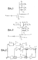
- FIG. 1 there is conventionally shown an RF transistor 1 for amplifying an input signal E having a high average P peak / P ratio.
- the output signal is available at S and the drain bias of the transistor by the voltage Vdrain is provided by a quarter wave line constituting a first decoupling stage D1 comprising a low loss RF capacitor C1 of sufficient value to present a short -circuit, a second decoupling stage D2 comprising a capacitor C2 of higher value than that of C1, capable of supplying current very quickly to transistor 1 during an abrupt rise in power of the signal E and a third decoupling stage D3 comprising a capacitor C3 capable of supplying a strong current for a longer time corresponding to a relatively long power peak consecutive to the presence of low frequency components in the input signal E.
- the capacitors C1, C2, C3 can have respective values of 68 pF, 1000 pF and a few tens of ⁇ F.
- the drain voltage of transistor 1 is provided from two separate supply voltages V1 and V2 respectively, the voltage V2 being greater than the voltage V1.
- This switch 2 makes it possible to apply to the drain of transistor 1, just upstream of the second decoupling stage D2, either the higher (V2) of the two voltages, via the third decoupling stage D3, or the lower (V1) via a fourth decoupling stage D4 comprising a capacitor C4 constituting a long-term charge reservoir ensuring the stability of the drain voltage for a significant period of time.
- the switch 2 is controlled by a control circuit 3 connected to the input E of the amplifier via a signal envelope detection circuit 4.
- the third decoupling stage D3 ensuring the drain a strong current for the time required which can be relatively long, while during the periods off peaks the switch is controlled to apply the lower voltage V1 by replacing stage D3 with the fourth stage D4, which is more appropriate to the situation and capable of ensuring the stability of the drain voltage over a long period which can reach 90% of the time of the amplifier.
- the components 2, C2, C3, C4 constituting all of the decoupling and charge storage stages according to the invention are chosen for their qualities of low inductance and of low internal resistance limiting the parasites generated and are integrated as closely as possible. of transistor 1 in order to ensure very fast and nevertheless clean switching operations.
- the switching system of the invention can be generalized to more than two voltages, with each voltage being associated with a specific decoupling stage, so as to modulate the supply voltage of the amplifier at the rate of l 'envelope of signal E so as to optimize the yield.
- the amplifier requires a high linearity of the output signal S, it is advantageously possible to associate with the device of the invention a correction of the feedforward type which will make it possible to further reduce disturbances such as noise or intermodulation.
- FIG. 3 illustrates such an application of the invention.
- the main amplifier stage receiving at E the input signal and delivering at S the output signal.
- the amplifier stage 1 integrates the decoupling stages D1 to D4 and the switch 2 in FIG. 2 and is connected to the supply voltages V1 and V2.
- the switch 2 integrated in stage 1 ′ is controlled by a control circuit 3 also receiving the input signal E via an envelope detection circuit 4.
- a sample of the signal S is taken at the output of the main amplifier 1 'and compared to the input signal E in a coupler 5.
- the result of this comparison called the error signal, consists of the distortion undergone by the signal and noise introduced by the main amplifier 1 '.
- This error signal is then amplified by a so-called error amplifier 6, its phase is rotated by 180 °, then it is reinjected using a coupler 7 on the main path of the output signal S so as to cancel the distortion. All the delays introduced by the various amplifiers are compensated by delay lines 8 so as to make the cancellation independent of the frequency.
Landscapes
- Engineering & Computer Science (AREA)
- Power Engineering (AREA)
- Physics & Mathematics (AREA)
- Nonlinear Science (AREA)
- Amplifiers (AREA)
- Transmitters (AREA)
Abstract
Description
La présente invention se rapporte aux amplificateurs de puissance utilisés dans les émetteurs de radiotéléphones dits de troisième génération ou de radiodiffusion numérique et plus généralement aux amplificateurs de puissance supportant des signaux présentant des écarts importants entre la puissance crête et la puissance moyenne pouvant atteindre un rapport de 10/1.The present invention relates to power amplifiers used in transmitters of so-called third generation radiotelephones or digital broadcasting and more generally to power amplifiers carrying signals having significant differences between the peak power and the average power which can reach a ratio of 10/1.
Ce type de modulation génère des écarts importants entre la puissance de crête des signaux et la puissance moyenne qui peuvent atteindre un rapport de 10/1.This type of modulation generates significant differences between the peak power of the signals and the average power which can reach a ratio of 10/1.
Dans de tels systèmes de transmission, si l'on veut que le signal de sortie soit une réplique exacte du signal d'entrée, autrement dit si l'on veut réaliser une amplification linéaire, il faut que l'amplificateur puisse amplifier aussi bien les crêtes que les signaux les plus faibles. C'est ainsi que, par exemple, pour émettre une puissance moyenne de 20 watts il faut un amplificateur de 200 watts. Malheureusement cet amplificateur de 200 watts n'émettra que 20 watts en moyenne, avec un rendement très inférieur à son rendement optimal, puisque, comme l'on sait, le rendement électrique, c'est-à-dire le rapport puissance de sortie / puissance consommée, n'est maximum que lorsque l'amplificateur fonctionne au maximum de sa puissance, à savoir lorsque son gain commence à décroître.In such transmission systems, if you want the output signal to be an exact replica of the input signal, in other words if you want to achieve linear amplification, the amplifier must be able to amplify the peaks as the weakest signals. Thus, for example, to transmit an average power of 20 watts you need an amplifier of 200 watts. Unfortunately this 200 watt amplifier will only emit 20 watts on average, with a yield much lower than its optimal efficiency, since, as we know, the electrical efficiency, that is to say the power output / power consumption, is maximum only when the amplifier operates at its maximum power, namely when its gain begins to decrease.
C'est ainsi qu'avec un tel amplificateur, pour un signal de puissance signal de crête / puissance signal moyen (P crête / P moyen) de 10 dB on peut obtenir un rendement de seulement 15 %, qui est néanmoins considéré comme excellent.Thus with such an amplifier, for a signal of peak signal power / average signal power (P peak / average P) of 10 dB it is possible obtain a yield of only 15%, which is nevertheless considered excellent.
Jusqu'à maintenant la plupart des efforts pour améliorer le rendement se sont concentrés sur la réduction du rapport P crête / P moyen en modifiant les modulations ou en utilisant des techniques digitales afin de diminuer les crêtes.To date, most efforts to improve yield have focused on reducing the average P peak / P ratio by modulating the modulations or using digital techniques to decrease the peaks.
Cependant on sait depuis longtemps que si l'on arrive à moduler la tension d'alimentation de l'amplificateur radiofréquence (RF) au rythme de l'enveloppe du signal, on peut gagner en rendement. Une telle modulation, appelée "enveloppe tracking" est décrite dans l'article de F.H. RAAB (F.H. RAAB, High efficiency amplification techniques, IEEE Circuits & Systems Journal, N° 7, Décembre 1975, pages 3 - 11) où un amplificateur en classe S est utilisé pour fournir une tension d'alimentation variable.However, we have known for a long time that if we manage to modulate the supply voltage of the radio frequency (RF) amplifier at the rate of the signal envelope, we can gain in efficiency. Such modulation, called "envelope tracking" is described in the article by FH RAAB (FH RAAB, High efficiency amplification techniques, IEEE Circuits & Systems Journal, N ° 7, December 1975, pages 3 - 11) where an amplifier in class S is used to supply a variable supply voltage.
D'autres auteurs ont proposé d'utiliser un convertisseur DC - DC dont on peut faire varier la tension de sortie pour alimenter l'amplificateur. Mais dans ce cas comme dans beaucoup d'autres on est limité à des vitesses de variation de la tension de l'ordre du MHz.Other authors have proposed using a DC-DC converter, the output voltage of which can be varied to supply the amplifier. But in this case, as in many others, we are limited to rates of variation of the voltage on the order of MHz.
Par ailleurs, la demande de brevet US publiée N° 2002/0094795 enseigne que la meilleure façon de passer d'une tension à une autre rapidement est en fait de commuter plusieurs alimentations distinctes.Furthermore, the published US patent application No. 2002/0094795 teaches that the best way to switch from one voltage to another quickly is in fact to switch several separate power supplies.
Toutefois, ces commutations générant des sauts d'amplitude et de phase, il est proposé de compenser ces sauts par une pré-correction.However, these commutations generating amplitude and phase jumps, it is proposed to compensate for these jumps by a pre-correction.
Cette technique néanmoins soulève quelques problèmes.This technique nevertheless raises some problems.
Il n'est pas aisé en effet de commuter deux alimentations de tensions distinctes car tous les amplificateurs radiofréquences de puissance nécessitent des condensateurs de forte valeur sur les drains des transistors afin d'assurer leur linéarité. Il est très courant par exemple de voir des capacités de 100 µF. Charger un condensateur de 100 µF de 10 V en 1 µs nécessite un courant de 1 000 A. Or les signaux modernes ont souvent des enveloppes qui varient beaucoup plus vite que cela (UMTS = 5 MHz = 200ns).It is not easy in fact to switch two separate voltage supplies because all radio frequency power amplifiers require high-value capacitors on the drains of the transistors in order to ensure their linearity. It is very common for example to see capacities of 100 µF. Charging a 100 µF 10 V capacitor in 1 µs requires a current of 1000 A. Now modern signals often have envelopes which vary much faster than that (UMTS = 5 MHz = 200ns).
Même si l'on arrive à diminuer les résistances de façon à faire passer ces courants, un second problème est que ces commutations sont de moins en moins propres lorsque celles-ci sont de plus en plus rapides. Les inductances parasites même minimes provoquent en effet des rebondissements des tensions d'alimentation. Ces rebondissements provoquent à leur tour une détérioration du signal de sortie (bruit, intermodulation, ...).Even if we manage to decrease the resistances so as to pass these currents, a second problem is that these commutations are less less clean when they are faster and faster. Even parasitic inductances, even minimal, cause rebounds in supply voltages. These twists in turn cause a deterioration of the output signal (noise, intermodulation, ...).
La précorrection est une technique efficace pour des régimes établis mais plus difficile à appliquer sur des régimes transitoires de vitesse élevée.Pre-correction is an effective technique for established regimes but more difficult to apply to transient high-speed regimes.
La demande de brevet US publiée N° 2002/0094795 propose d'utiliser des modulateurs d'amplitude et de phase afin d'appliquer une telle pré-correction. Il va dès lors se poser le problème de la vitesse et de la linéarité des modulateurs, à supposer qu'il n'y ait pas de phénomène de mémoire.The published US patent application No. 2002/0094795 proposes to use amplitude and phase modulators in order to apply such pre-correction. The problem of speed and linearity of the modulators will therefore arise, assuming that there is no memory phenomenon.
La présente invention vise à moduler la tension d'alimentation de l'amplificateur RF par commutation de tension mais de manière que cette commutation soit plus propre, c'est-à-dire avec le moins possible d'inductances parasites, en sorte de provoquer le moins de perturbations possible du signal de sortie.The present invention aims to modulate the supply voltage of the RF amplifier by voltage switching but in such a way that this switching is cleaner, that is to say with the least possible parasitic inductances, so as to cause the least possible disturbance of the output signal.
A cet effet, l'invention a pour objet un amplificateur de puissance pour systèmes de transmission radiofréquences, dont le signal présente un rapport P crête/P moyen élevé, comprenant un étage d'amplification final à transistor à commutation de tension de drain sur au moins deux tensions d'alimentation distinctes, la polarisation de drain étant constituée d'un premier étage de découplage formé d'une ligne quart d'onde suivie d'un deuxième étage de découplage apte à fournir un courant rapidement lors d'une brusque montée en puissance du signal et d'un troisième étage de découplage apte à fournir un courant fort lors de pics de puissance relativement longs, caractérisé en ce que ledit troisième étage intègre un étage de commutation de tension, interposé entre lesdits troisième et deuxième étages et apte à commuter sur le drain l'une quelconque desdites tensions d'alimentation distinctes en sorte que l'ensemble troisième étage de découplage - étage de commutation constitue des réservoirs de charge appropriés à toutes les tensions d'alimentation, permettant à la fois d'assurer la stabilité de la tension du drain pendant les périodes de temps hors crêtes du signal d'entrée et d'assurer un approvisionnement en courant suffisant dudit transistor pendant les crêtes.To this end, the invention relates to a power amplifier for radio frequency transmission systems, the signal of which has a high average P peak / P ratio, comprising a final amplification stage with transistor with drain voltage switching on at at least two separate supply voltages, the drain polarization consisting of a first decoupling stage formed by a quarter-wave line followed by a second decoupling stage capable of supplying a current rapidly during an abrupt rise in signal power and of a third decoupling stage capable of supplying a strong current during relatively long power peaks, characterized in that said third stage incorporates a voltage switching stage, interposed between said third and second stages and suitable switching any of said separate supply voltages to the drain so that the third decoupling stage - stage switching constitutes charge reservoirs suitable for all supply voltages, making it possible both to ensure the stability of the drain voltage during periods of time outside peaks of the input signal and ensuring a sufficient current supply of said transistor during peaks.
Suivant une application de l'invention à la commutation de deux tensions d'alimentation distinctes, l'étage de commutation est agencé en sorte de commuter sur le drain la tension d'alimentation la plus élevée en même temps que ledit troisième étage de découplage et la tension d'alimentation la moins élevée en même temps qu'un quatrième étage de découplage constituant un réservoir de charge à long terme assurant la stabilité de la tension drain.According to an application of the invention to the switching of two separate supply voltages, the switching stage is arranged so as to switch the highest supply voltage on the drain at the same time as said third decoupling stage and the lowest supply voltage at the same time as a fourth decoupling stage constituting a long-term charge reservoir ensuring the stability of the drain voltage.
Suivant une variante de réalisation de l'invention appliquée à la réalisation d'un amplificateur requérant une linéarité importante du signal de sortie, l'étage de sortie dudit amplificateur comporte une boucle de réaction amont dénommée feedforward en sorte de corriger les perturbations transitoires rapides provoquées par les commutations de tension d'alimentation dudit étage de sortie.According to an alternative embodiment of the invention applied to the production of an amplifier requiring a high linearity of the output signal, the output stage of said amplifier comprises an upstream feedback loop called feedforward so as to correct the rapid transient disturbances caused by the supply voltage switches of said output stage.
L'utilisation d'une telle boucle, connue en elle-même, en combinaison avec l'étage de commutation de tension, est particulièrement judicieuse et intéressante car elle permet, conformément à l'invention, de réduire très sensiblement le bruit et l'intermodulation, qui est la caractéristique bien connue du feedforward, mais en éliminant l'inconvénient également bien connu d'un tel système à savoir sa vulnérabilité à la compression de gain de l'amplificateur lors des crêtes de puissance, cet inconvénient étant, dans le cadre de la présente invention, pratiquement supprimé, la compression de gain étant compensée par la commutation de tension sur ledit amplificateur. La puissance crête sera ainsi améliorée en même temps que le rendement.The use of such a loop, known in itself, in combination with the voltage switching stage, is particularly judicious and advantageous because it allows, in accordance with the invention, to very significantly reduce noise and intermodulation, which is the well-known characteristic of feedforward, but by eliminating the equally well-known drawback of such a system, namely its vulnerability to amplifier gain compression during power peaks, this drawback being, in the part of the present invention, practically eliminated, the gain compression being compensated for by the voltage switching on said amplifier. The peak power will thus be improved at the same time as the efficiency.
Selon un mode de réalisation particulier de l'invention, l'étage de commutation de tension est commandé par un circuit de commande relié à l'entrée de l'amplificateur via un circuit de détection d'enveloppe du signal.According to a particular embodiment of the invention, the voltage switching stage is controlled by a control circuit connected to the input of the amplifier via a signal envelope detection circuit.
Plus particulièrement, le commutateur peut commuter plus de deux tensions, à chaque tension étant associé un étage de découplage spécifique, en sorte de moduler la tension d'alimentation de l'amplificateur au rythme de l'enveloppe du signal.More particularly, the switch can switch more than two voltages, with each voltage being associated with a specific decoupling stage, so as to modulate the supply voltage of the amplifier at the rate of the signal envelope.
Selon un mode de réalisation particulier de l'invention, le commutateur est intégré dans le dernier étage de découplage de l'amplificateur, les composants constitutifs de l'ensemble des étages de découplage et de stockage de charges étant intégrés au plus près du transistor.According to a particular embodiment of the invention, the switch is integrated in the last decoupling stage of the amplifier, the constituent components of all of the decoupling and charge storage stages being integrated as close as possible to the transistor.
On va maintenant décrire un mode de mise en oeuvre du dispositif de l'invention, en référence au dessin annexé sur lequel :
- la figure 1 est un schéma de polarisation conventionnelle d'un étage final d'amplificateur RF ;
- la figure 2 représente le schéma de la figure 1 intégrant l'étage de commutation de tension selon l'invention, et
- la figure 3 est un schéma d'un amplificateur selon l'invention, intégrant l'étage de commutation de tension ainsi qu'une boucle feedforward.
- Figure 1 is a conventional polarization diagram of a final stage of RF amplifier;
- FIG. 2 represents the diagram of FIG. 1 integrating the voltage switching stage according to the invention, and
- Figure 3 is a diagram of an amplifier according to the invention, integrating the voltage switching stage as well as a feedforward loop.
Sur la figure 1, on a représenté conventionnellement un transistor RF 1 d'amplification d'un signal d'entrée E présentant un rapport P crête/P moyen élevé. Le signal de sortie est disponible en S et la polarisation de drain du transistor par la tension Vdrain est assurée par une ligne quart d'onde constituant un premier étage D1 de découplage comprenant un condensateur RF à faibles pertes C1 de valeur suffisante pour présenter un court-circuit, un deuxième étage D2 de découplage comprenant un condensateur C2 de valeur plus élevée que celle de C1, capable de fournir du courant très rapidement au transistor 1 lors d'une brusque montée en puissance du signal E et un troisième étage D3 de découplage comprenant un condensateur C3 apte à fournir un courant fort pendant un temps plus long correspondant à un pic de puissance relativement long consécutif à la présence de composantes basses fréquences dans le signal d'entrée E.In FIG. 1, there is conventionally shown an
A titre indicatif, pour un amplificateur à 2GHz, les condensateurs C1, C2, C3 peuvent avoir des valeurs respectives de 68 pF, 1 000 pF et quelques dizaines de µF.As an indication, for a 2GHz amplifier, the capacitors C1, C2, C3 can have respective values of 68 pF, 1000 pF and a few tens of µF.
Conformément à l'invention, la tension de drain du transistor 1 est assurée à partir de deux tensions d'alimentation distinctes respectivement V1 et V2, la tension V2 étant supérieure à la tension V1.According to the invention, the drain voltage of
L'une ou l'autre de ces tensions est appliquée au drain via un commutateur symbolisé en 2, intégré au troisième étage D3.Either of these voltages is applied to the drain via a switch symbolized at 2, integrated into the third stage D3.
Ce commutateur 2 permet d'appliquer au drain du transistor 1, juste en amont du deuxième étage de découplage D2, soit la plus forte (V2) des deux tensions, via le troisième étage de découplage D3, soit la plus faible (V1) via un quatrième étage de découplage D4 comprenant un condensateur C4 constituant un réservoir de charge à long terme assurant la stabilité de la tension drain pendant un laps de temps important.This
Le commutateur 2 est commandé par un circuit de commande 3 relié à l'entrée E de l'amplificateur via un circuit de 4 détection d'enveloppe du signal.The
Ainsi, lors de la détection de crêtes de puissance, c'est la tension V2 qui sera commutée sur le drain, le troisième étage de découplage D3 assurant au drain un courant fort le temps nécessaire qui peut être relativement long, alors que pendant les périodes hors crêtes le commutateur est commandé pour appliquer la tension inférieure V1 en substituant à l'étage D3 le quatrième étage D4, plus approprié à la situation et apte à assurer la stabilité de la tension drain sur une longue période qui peut atteindre 90 % du temps de fonctionnement de l'amplificateur.Thus, during the detection of power peaks, it is the voltage V2 which will be switched on the drain, the third decoupling stage D3 ensuring the drain a strong current for the time required which can be relatively long, while during the periods off peaks the switch is controlled to apply the lower voltage V1 by replacing stage D3 with the fourth stage D4, which is more appropriate to the situation and capable of ensuring the stability of the drain voltage over a long period which can reach 90% of the time of the amplifier.
On obtient ainsi un fonctionnement de l'amplificateur avec un rendement sensiblement plus intéressant tout en opérant une commutation propre en particulier par rapport à celle réalisée dans la demande de brevet US publiée N° 2002/0094795, grâce à l'intégration du commutateur dans le dernier étage de découplage (D3, D4) de l'amplificateur. Une telle intégration réduit substantiellement, notamment lorsque les commutations de tension sont très rapides, les inductances parasites qui induisent des détériorations (bruit, intermodulation) du signal de sortie S.One thus obtains an operation of the amplifier with a substantially more interesting yield while operating its own switching in particular compared to that carried out in the US patent application published N ° 2002/0094795, thanks to the integration of the switch in the last decoupling stage (D3, D4) of the amplifier. Such integration substantially reduces, especially when the voltage switching is very fast, the parasitic inductances which induce deterioration (noise, intermodulation) of the output signal S.
Les composants 2, C2, C3, C4 constitutifs de l'ensemble des étages de découplage et de stockage de charges selon l'invention sont choisis pour leur qualités de faible inductance et de faible résistance interne limitant les parasites générés et sont intégrés au plus près du transistor 1 afin d'assurer des commutations très rapides et néanmoins propres.The
Il est à noter que le système de commutation de l'invention peut être généralisé à plus de deux tensions, à chaque tension étant associé un étage de découplage spécifique, en sorte de moduler la tension d'alimentation de l'amplificateur au rythme de l'enveloppe du signal E en sorte d'optimiser le rendement.It should be noted that the switching system of the invention can be generalized to more than two voltages, with each voltage being associated with a specific decoupling stage, so as to modulate the supply voltage of the amplifier at the rate of l 'envelope of signal E so as to optimize the yield.
Par ailleurs, si l'amplificateur requiert une linéarité importante du signal de sortie S on peut avantageusement associer au dispositif de l'invention une correction de type feedforward qui va permettre de réduire encore plus les perturbations telles que le bruit ou l'intermodulation.Furthermore, if the amplifier requires a high linearity of the output signal S, it is advantageously possible to associate with the device of the invention a correction of the feedforward type which will make it possible to further reduce disturbances such as noise or intermodulation.
La figure 3 illustre une telle application de l'invention. En 1' est représenté l'étage amplificateur principal recevant en E le signal d'entrée et délivrant en S le signal de sortie. L'étage amplificateur 1' intègre les étages de découplage D1 à D4 et le commutateur 2 de la figure 2 et est connecté aux tensions d'alimentation V1 et V2.FIG. 3 illustrates such an application of the invention. In 1 'is shown the main amplifier stage receiving at E the input signal and delivering at S the output signal. The amplifier stage 1 'integrates the decoupling stages D1 to D4 and the
Le commutateur 2 intégré à l'étage 1' est commandé par un circuit de commande 3 recevant également le signal d'entrée E via un circuit 4 de détection d'enveloppe.The
Un échantillon du signal S est prélevé à la sortie de l'amplificateur principal 1' et comparé au signal d'entrée E dans un coupleur 5. Le résultat de cette comparaison, appelé signal d'erreur, est constitué de la distorsion subie par le signal et du bruit introduit par l'amplificateur principal 1'.A sample of the signal S is taken at the output of the main amplifier 1 'and compared to the input signal E in a
Ce signal d'erreur est alors amplifié par un amplificateur dit d'erreur 6, sa phase est tournée de 180°, puis il est réinjecté à l'aide d'un coupleur 7 sur le chemin principal du signal de sortie S de manière à produire une annulation de la distorsion. Tous les retards introduits par les divers amplificateurs sont compensés par des lignes à retard 8 de manière à rendre l'annulation indépendante de la fréquence.This error signal is then amplified by a so-called
Le principe de linéarisation du signal de sortie par une boucle de réaction amont du type feedforward est bien connu.The principle of linearization of the output signal by an upstream feedback loop of the feedforward type is well known.
Cependant, l'inconvénient intrinsèque du feedforward, également bien connu, est la compression de gain de l'amplificateur lors des crêtes de puissance.However, the intrinsic drawback of the feedforward, also well known, is the gain compression of the amplifier during power peaks.
Mais cet inconvénient du feedforward est de manière tout à fait judicieuse supprimé grâce à l'association du feedforward à l'étage de commutation (2, D3, D4) intégré conformément à l'invention, dans l'amplificateur principal 1', lequel étage de commutation réduit les crêtes de puissance et met donc le feedforward dans des conditions évitant la manifestation desdits inconvénients du feedforward.However, this disadvantage of the feedforward is quite judiciously eliminated by virtue of the association of the feedforward with the switching stage (2, D3, D4) integrated in accordance with the invention, in the main amplifier 1 ', which stage switching reduces power peaks and therefore puts the feedforward in conditions avoiding the manifestation of said disadvantages of the feedforward.
On améliore ainsi, tout à la fois la puissance crête (réduction du rapport P crête / P moyen), le rendement et la linéarité de l'amplificateur principal.This improves both the peak power (reduction of the average P peak / P ratio), the efficiency and the linearity of the main amplifier.
Claims (6)
Applications Claiming Priority (2)
| Application Number | Priority Date | Filing Date | Title |
|---|---|---|---|
| FR0213381 | 2002-10-25 | ||
| FR0213381A FR2846489B1 (en) | 2002-10-25 | 2002-10-25 | POWER AMPLIFIER FOR RADIO FREQUENCY TRANSMISSION SYSTEMS |
Publications (2)
| Publication Number | Publication Date |
|---|---|
| EP1414148A1 true EP1414148A1 (en) | 2004-04-28 |
| EP1414148B1 EP1414148B1 (en) | 2008-08-13 |
Family
ID=32050675
Family Applications (1)
| Application Number | Title | Priority Date | Filing Date |
|---|---|---|---|
| EP03362020A Expired - Lifetime EP1414148B1 (en) | 2002-10-25 | 2003-10-23 | Power amplifier for radio frequency transmission systems |
Country Status (4)
| Country | Link |
|---|---|
| EP (1) | EP1414148B1 (en) |
| AT (1) | ATE405028T1 (en) |
| DE (1) | DE60322812D1 (en) |
| FR (1) | FR2846489B1 (en) |
Citations (6)
| Publication number | Priority date | Publication date | Assignee | Title |
|---|---|---|---|---|
| JPS574607A (en) * | 1980-06-11 | 1982-01-11 | Fujitsu Ltd | High-frequency amplifier |
| EP0524772A2 (en) * | 1991-07-23 | 1993-01-27 | Matra Marconi Space UK Limited | Microwave power amplifiers |
| EP0673112A1 (en) * | 1994-03-14 | 1995-09-20 | Matsushita Electronics Corporation | Power amplifier and power amplification method |
| US6008698A (en) * | 1998-05-18 | 1999-12-28 | Omnipoint Corporation | Amplifier with dynamically adaptable supply current |
| US20020014920A1 (en) * | 2000-07-14 | 2002-02-07 | Masami Ohnishi | High frequency power amplifier |
| WO2002017478A1 (en) * | 2000-08-24 | 2002-02-28 | Nokia Corporation | Power amplifier arrangement |
-
2002
- 2002-10-25 FR FR0213381A patent/FR2846489B1/en not_active Expired - Fee Related
-
2003
- 2003-10-23 EP EP03362020A patent/EP1414148B1/en not_active Expired - Lifetime
- 2003-10-23 DE DE60322812T patent/DE60322812D1/en not_active Expired - Lifetime
- 2003-10-23 AT AT03362020T patent/ATE405028T1/en not_active IP Right Cessation
Patent Citations (6)
| Publication number | Priority date | Publication date | Assignee | Title |
|---|---|---|---|---|
| JPS574607A (en) * | 1980-06-11 | 1982-01-11 | Fujitsu Ltd | High-frequency amplifier |
| EP0524772A2 (en) * | 1991-07-23 | 1993-01-27 | Matra Marconi Space UK Limited | Microwave power amplifiers |
| EP0673112A1 (en) * | 1994-03-14 | 1995-09-20 | Matsushita Electronics Corporation | Power amplifier and power amplification method |
| US6008698A (en) * | 1998-05-18 | 1999-12-28 | Omnipoint Corporation | Amplifier with dynamically adaptable supply current |
| US20020014920A1 (en) * | 2000-07-14 | 2002-02-07 | Masami Ohnishi | High frequency power amplifier |
| WO2002017478A1 (en) * | 2000-08-24 | 2002-02-28 | Nokia Corporation | Power amplifier arrangement |
Non-Patent Citations (2)
| Title |
|---|
| "The PM2105 Power Amplifier. Application note 2594", 30 June 2000, PACIFIC MONOLITHICS, WWW.RFPOWERNET.COM, XP002241148 * |
| PATENT ABSTRACTS OF JAPAN vol. 006, no. 064 (E - 103) 23 April 1982 (1982-04-23) * |
Also Published As
| Publication number | Publication date |
|---|---|
| ATE405028T1 (en) | 2008-08-15 |
| DE60322812D1 (en) | 2008-09-25 |
| EP1414148B1 (en) | 2008-08-13 |
| FR2846489B1 (en) | 2005-03-25 |
| FR2846489A1 (en) | 2004-04-30 |
Similar Documents
| Publication | Publication Date | Title |
|---|---|---|
| EP0283074B1 (en) | Microwave mixer | |
| EP1940019B1 (en) | Linearisation device with pre-distortion with adjustable amplitude and curve | |
| FR2816132A1 (en) | Reconfigurable device for amplifying radio-frequency signals, comprising power divider, amplifier set and power combiner, controlled by measuring input and output powers | |
| FR2798244A1 (en) | HIGH EFFICIENCY POWER AMPLIFICATION CIRCUIT AND METHOD ALLOWING A WIDE RANGE OF DYNAMIC POWER REDUCTION | |
| EP1713177A1 (en) | Variable gain differential amplifier | |
| FR2558997A1 (en) | ELECTRIC SIGNAL GROUP PROPAGATION TIME CORRECTING AMPLIFIER AND INTERMEDIATE FREQUENCY AMPLIFICATION CHAIN OF RADIO BEAMS COMPRISING SUCH AMPLIFIER | |
| FR2826205A1 (en) | Amplitude modulation system for e.g. a transmitter of a mobile station includes power amplifier with automatic gain control system | |
| EP3381123B1 (en) | Dc-to-dc converter block with multiple supply voltages, multi-supply-voltage dc-to-dc converter comprising same, and associated envelope tracking system | |
| EP0549043A1 (en) | Integrated circuit comprising an amplifier with variable gain | |
| EP1414148B1 (en) | Power amplifier for radio frequency transmission systems | |
| FR2844066A1 (en) | Control of quiescent currents in a direct frequency converter used in mobile telephones, uses closed loop regulation of common-mode quiescent current so it tracks reference current | |
| EP2543136B1 (en) | Current-voltage converter having a current reflector, input stage of an amplifier and corresponding amplifier | |
| EP0060164B1 (en) | Sliding class a broadband linear amplifier with low power consumption, and circuit comprising at least one such amplifier | |
| EP3824549A1 (en) | Rf radio frequency transmitter architecture | |
| EP2182631A2 (en) | Broadband microwave frequency amplifier cell with variable gain and amplifier comprising such a cell | |
| EP0318379A1 (en) | Ultra-high frequency amplifier with a very wide pass band | |
| EP0078189A1 (en) | Hyperfrequency power transmitter with field effect transistors, particularly for Doppler radar | |
| EP0201964B1 (en) | Amplifier for high frequencies | |
| FR2873872A1 (en) | AUDIO CLASS AD AMPLIFIER | |
| FR2730363A1 (en) | HIGH FREQUENCY HIGH GAIN AMPLIFIER AND RESONANT CIRCUIT OSCILLATOR PROVIDED WITH SUCH AMPLIFIER | |
| FR2696295A1 (en) | Non-linear distortion correction appts. for amplifier partic. for satellite communications - separates incoming signal to two electronic circuits which reflect signals for recombination | |
| FR2744304A1 (en) | Digital=analog converter using current source | |
| EP1039652B1 (en) | Antenna arrangement | |
| EP1251634A1 (en) | Transconductance stage and RF communications device including such a stage | |
| FR2768277A1 (en) | TRANSMITTER HAVING IMPROVED ADDITIONAL POWER OUTPUT AND RADIO EMPLOYING SAME |
Legal Events
| Date | Code | Title | Description |
|---|---|---|---|
| PUAI | Public reference made under article 153(3) epc to a published international application that has entered the european phase |
Free format text: ORIGINAL CODE: 0009012 |
|
| AK | Designated contracting states |
Kind code of ref document: A1 Designated state(s): AT BE BG CH CY CZ DE DK EE ES FI FR GB GR HU IE IT LI LU MC NL PT RO SE SI SK TR |
|
| AX | Request for extension of the european patent |
Extension state: AL LT LV MK |
|
| 17P | Request for examination filed |
Effective date: 20040924 |
|
| AKX | Designation fees paid |
Designated state(s): AT BE BG CH CY CZ DE DK EE ES FI FR GB GR HU IE IT LI LU MC NL PT RO SE SI SK TR |
|
| GRAP | Despatch of communication of intention to grant a patent |
Free format text: ORIGINAL CODE: EPIDOSNIGR1 |
|
| GRAS | Grant fee paid |
Free format text: ORIGINAL CODE: EPIDOSNIGR3 |
|
| GRAA | (expected) grant |
Free format text: ORIGINAL CODE: 0009210 |
|
| AK | Designated contracting states |
Kind code of ref document: B1 Designated state(s): AT BE BG CH CY CZ DE DK EE ES FI FR GB GR HU IE IT LI LU MC NL PT RO SE SI SK TR |
|
| REG | Reference to a national code |
Ref country code: GB Ref legal event code: FG4D Free format text: NOT ENGLISH |
|
| REG | Reference to a national code |
Ref country code: CH Ref legal event code: EP |
|
| REG | Reference to a national code |
Ref country code: IE Ref legal event code: FG4D Free format text: LANGUAGE OF EP DOCUMENT: FRENCH |
|
| REF | Corresponds to: |
Ref document number: 60322812 Country of ref document: DE Date of ref document: 20080925 Kind code of ref document: P |
|
| REG | Reference to a national code |
Ref country code: SE Ref legal event code: TRGR |
|
| PG25 | Lapsed in a contracting state [announced via postgrant information from national office to epo] |
Ref country code: ES Free format text: LAPSE BECAUSE OF FAILURE TO SUBMIT A TRANSLATION OF THE DESCRIPTION OR TO PAY THE FEE WITHIN THE PRESCRIBED TIME-LIMIT Effective date: 20081124 Ref country code: NL Free format text: LAPSE BECAUSE OF FAILURE TO SUBMIT A TRANSLATION OF THE DESCRIPTION OR TO PAY THE FEE WITHIN THE PRESCRIBED TIME-LIMIT Effective date: 20080813 |
|
| PG25 | Lapsed in a contracting state [announced via postgrant information from national office to epo] |
Ref country code: SI Free format text: LAPSE BECAUSE OF FAILURE TO SUBMIT A TRANSLATION OF THE DESCRIPTION OR TO PAY THE FEE WITHIN THE PRESCRIBED TIME-LIMIT Effective date: 20080813 Ref country code: AT Free format text: LAPSE BECAUSE OF FAILURE TO SUBMIT A TRANSLATION OF THE DESCRIPTION OR TO PAY THE FEE WITHIN THE PRESCRIBED TIME-LIMIT Effective date: 20080813 Ref country code: FI Free format text: LAPSE BECAUSE OF FAILURE TO SUBMIT A TRANSLATION OF THE DESCRIPTION OR TO PAY THE FEE WITHIN THE PRESCRIBED TIME-LIMIT Effective date: 20080813 |
|
| REG | Reference to a national code |
Ref country code: IE Ref legal event code: FD4D |
|
| BERE | Be: lapsed |
Owner name: LPA CONCEPTS Effective date: 20081031 |
|
| PG25 | Lapsed in a contracting state [announced via postgrant information from national office to epo] |
Ref country code: DK Free format text: LAPSE BECAUSE OF FAILURE TO SUBMIT A TRANSLATION OF THE DESCRIPTION OR TO PAY THE FEE WITHIN THE PRESCRIBED TIME-LIMIT Effective date: 20080813 Ref country code: BG Free format text: LAPSE BECAUSE OF FAILURE TO SUBMIT A TRANSLATION OF THE DESCRIPTION OR TO PAY THE FEE WITHIN THE PRESCRIBED TIME-LIMIT Effective date: 20081113 Ref country code: IE Free format text: LAPSE BECAUSE OF FAILURE TO SUBMIT A TRANSLATION OF THE DESCRIPTION OR TO PAY THE FEE WITHIN THE PRESCRIBED TIME-LIMIT Effective date: 20080813 |
|
| PG25 | Lapsed in a contracting state [announced via postgrant information from national office to epo] |
Ref country code: MC Free format text: LAPSE BECAUSE OF NON-PAYMENT OF DUE FEES Effective date: 20081031 Ref country code: SK Free format text: LAPSE BECAUSE OF FAILURE TO SUBMIT A TRANSLATION OF THE DESCRIPTION OR TO PAY THE FEE WITHIN THE PRESCRIBED TIME-LIMIT Effective date: 20080813 Ref country code: RO Free format text: LAPSE BECAUSE OF FAILURE TO SUBMIT A TRANSLATION OF THE DESCRIPTION OR TO PAY THE FEE WITHIN THE PRESCRIBED TIME-LIMIT Effective date: 20080813 Ref country code: PT Free format text: LAPSE BECAUSE OF FAILURE TO SUBMIT A TRANSLATION OF THE DESCRIPTION OR TO PAY THE FEE WITHIN THE PRESCRIBED TIME-LIMIT Effective date: 20090113 Ref country code: CZ Free format text: LAPSE BECAUSE OF FAILURE TO SUBMIT A TRANSLATION OF THE DESCRIPTION OR TO PAY THE FEE WITHIN THE PRESCRIBED TIME-LIMIT Effective date: 20080813 |
|
| REG | Reference to a national code |
Ref country code: CH Ref legal event code: PL |
|
| PLBE | No opposition filed within time limit |
Free format text: ORIGINAL CODE: 0009261 |
|
| STAA | Information on the status of an ep patent application or granted ep patent |
Free format text: STATUS: NO OPPOSITION FILED WITHIN TIME LIMIT |
|
| 26N | No opposition filed |
Effective date: 20090514 |
|
| PG25 | Lapsed in a contracting state [announced via postgrant information from national office to epo] |
Ref country code: EE Free format text: LAPSE BECAUSE OF FAILURE TO SUBMIT A TRANSLATION OF THE DESCRIPTION OR TO PAY THE FEE WITHIN THE PRESCRIBED TIME-LIMIT Effective date: 20080813 |
|
| PG25 | Lapsed in a contracting state [announced via postgrant information from national office to epo] |
Ref country code: IT Free format text: LAPSE BECAUSE OF FAILURE TO SUBMIT A TRANSLATION OF THE DESCRIPTION OR TO PAY THE FEE WITHIN THE PRESCRIBED TIME-LIMIT Effective date: 20080813 |
|
| PG25 | Lapsed in a contracting state [announced via postgrant information from national office to epo] |
Ref country code: BE Free format text: LAPSE BECAUSE OF NON-PAYMENT OF DUE FEES Effective date: 20081031 |
|
| PG25 | Lapsed in a contracting state [announced via postgrant information from national office to epo] |
Ref country code: LI Free format text: LAPSE BECAUSE OF NON-PAYMENT OF DUE FEES Effective date: 20081031 Ref country code: CH Free format text: LAPSE BECAUSE OF NON-PAYMENT OF DUE FEES Effective date: 20081031 |
|
| PG25 | Lapsed in a contracting state [announced via postgrant information from national office to epo] |
Ref country code: LU Free format text: LAPSE BECAUSE OF NON-PAYMENT OF DUE FEES Effective date: 20081023 Ref country code: HU Free format text: LAPSE BECAUSE OF FAILURE TO SUBMIT A TRANSLATION OF THE DESCRIPTION OR TO PAY THE FEE WITHIN THE PRESCRIBED TIME-LIMIT Effective date: 20090214 Ref country code: CY Free format text: LAPSE BECAUSE OF FAILURE TO SUBMIT A TRANSLATION OF THE DESCRIPTION OR TO PAY THE FEE WITHIN THE PRESCRIBED TIME-LIMIT Effective date: 20080813 |
|
| PG25 | Lapsed in a contracting state [announced via postgrant information from national office to epo] |
Ref country code: TR Free format text: LAPSE BECAUSE OF FAILURE TO SUBMIT A TRANSLATION OF THE DESCRIPTION OR TO PAY THE FEE WITHIN THE PRESCRIBED TIME-LIMIT Effective date: 20080813 |
|
| PG25 | Lapsed in a contracting state [announced via postgrant information from national office to epo] |
Ref country code: GR Free format text: LAPSE BECAUSE OF FAILURE TO SUBMIT A TRANSLATION OF THE DESCRIPTION OR TO PAY THE FEE WITHIN THE PRESCRIBED TIME-LIMIT Effective date: 20081114 |
|
| REG | Reference to a national code |
Ref country code: FR Ref legal event code: PLFP Year of fee payment: 13 |
|
| REG | Reference to a national code |
Ref country code: FR Ref legal event code: PLFP Year of fee payment: 14 |
|
| PGFP | Annual fee paid to national office [announced via postgrant information from national office to epo] |
Ref country code: FR Payment date: 20161028 Year of fee payment: 14 Ref country code: DE Payment date: 20161024 Year of fee payment: 14 Ref country code: GB Payment date: 20161027 Year of fee payment: 14 |
|
| PGFP | Annual fee paid to national office [announced via postgrant information from national office to epo] |
Ref country code: SE Payment date: 20161027 Year of fee payment: 14 |
|
| REG | Reference to a national code |
Ref country code: DE Ref legal event code: R119 Ref document number: 60322812 Country of ref document: DE |
|
| REG | Reference to a national code |
Ref country code: SE Ref legal event code: EUG |
|
| GBPC | Gb: european patent ceased through non-payment of renewal fee |
Effective date: 20171023 |
|
| REG | Reference to a national code |
Ref country code: FR Ref legal event code: ST Effective date: 20180629 |
|
| PG25 | Lapsed in a contracting state [announced via postgrant information from national office to epo] |
Ref country code: DE Free format text: LAPSE BECAUSE OF NON-PAYMENT OF DUE FEES Effective date: 20180501 Ref country code: GB Free format text: LAPSE BECAUSE OF NON-PAYMENT OF DUE FEES Effective date: 20171023 |
|
| PG25 | Lapsed in a contracting state [announced via postgrant information from national office to epo] |
Ref country code: SE Free format text: LAPSE BECAUSE OF NON-PAYMENT OF DUE FEES Effective date: 20171024 Ref country code: FR Free format text: LAPSE BECAUSE OF NON-PAYMENT OF DUE FEES Effective date: 20171031 |