EP1414148A1 - Leistungsverstärker für Hochfrequenz-Transmissionssysteme - Google Patents
Leistungsverstärker für Hochfrequenz-Transmissionssysteme Download PDFInfo
- Publication number
- EP1414148A1 EP1414148A1 EP03362020A EP03362020A EP1414148A1 EP 1414148 A1 EP1414148 A1 EP 1414148A1 EP 03362020 A EP03362020 A EP 03362020A EP 03362020 A EP03362020 A EP 03362020A EP 1414148 A1 EP1414148 A1 EP 1414148A1
- Authority
- EP
- European Patent Office
- Prior art keywords
- stage
- amplifier
- voltage
- decoupling
- drain
- Prior art date
- Legal status (The legal status is an assumption and is not a legal conclusion. Google has not performed a legal analysis and makes no representation as to the accuracy of the status listed.)
- Granted
Links
Images
Classifications
-
- H—ELECTRICITY
- H03—ELECTRONIC CIRCUITRY
- H03F—AMPLIFIERS
- H03F1/00—Details of amplifiers with only discharge tubes, only semiconductor devices or only unspecified devices as amplifying elements
- H03F1/02—Modifications of amplifiers to raise the efficiency, e.g. gliding Class A stages, use of an auxiliary oscillation
- H03F1/0205—Modifications of amplifiers to raise the efficiency, e.g. gliding Class A stages, use of an auxiliary oscillation in transistor amplifiers
- H03F1/0211—Modifications of amplifiers to raise the efficiency, e.g. gliding Class A stages, use of an auxiliary oscillation in transistor amplifiers with control of the supply voltage or current
- H03F1/0244—Stepped control
-
- H—ELECTRICITY
- H03—ELECTRONIC CIRCUITRY
- H03F—AMPLIFIERS
- H03F1/00—Details of amplifiers with only discharge tubes, only semiconductor devices or only unspecified devices as amplifying elements
- H03F1/32—Modifications of amplifiers to reduce non-linear distortion
- H03F1/3223—Modifications of amplifiers to reduce non-linear distortion using feed-forward
-
- H—ELECTRICITY
- H03—ELECTRONIC CIRCUITRY
- H03F—AMPLIFIERS
- H03F3/00—Amplifiers with only discharge tubes or only semiconductor devices as amplifying elements
- H03F3/189—High frequency amplifiers, e.g. radio frequency amplifiers
- H03F3/19—High frequency amplifiers, e.g. radio frequency amplifiers with semiconductor devices only
- H03F3/193—High frequency amplifiers, e.g. radio frequency amplifiers with semiconductor devices only with field-effect devices
Definitions
- the present invention relates to power amplifiers used in transmitters of so-called third generation radiotelephones or digital broadcasting and more generally to power amplifiers carrying signals having significant differences between the peak power and the average power which can reach a ratio of 10/1.
- This type of modulation generates significant differences between the peak power of the signals and the average power which can reach a ratio of 10/1.
- the amplifier In such transmission systems, if you want the output signal to be an exact replica of the input signal, in other words if you want to achieve linear amplification, the amplifier must be able to amplify the peaks as the weakest signals. Thus, for example, to transmit an average power of 20 watts you need an amplifier of 200 watts. Unfortunately this 200 watt amplifier will only emit 20 watts on average, with a yield much lower than its optimal efficiency, since, as we know, the electrical efficiency, that is to say the power output / power consumption, is maximum only when the amplifier operates at its maximum power, namely when its gain begins to decrease.
- Pre-correction is an effective technique for established regimes but more difficult to apply to transient high-speed regimes.
- the present invention aims to modulate the supply voltage of the RF amplifier by voltage switching but in such a way that this switching is cleaner, that is to say with the least possible parasitic inductances, so as to cause the least possible disturbance of the output signal.
- the invention relates to a power amplifier for radio frequency transmission systems, the signal of which has a high average P peak / P ratio, comprising a final amplification stage with transistor with drain voltage switching on at at least two separate supply voltages, the drain polarization consisting of a first decoupling stage formed by a quarter-wave line followed by a second decoupling stage capable of supplying a current rapidly during an abrupt rise in signal power and of a third decoupling stage capable of supplying a strong current during relatively long power peaks, characterized in that said third stage incorporates a voltage switching stage, interposed between said third and second stages and suitable switching any of said separate supply voltages to the drain so that the third decoupling stage - stage switching constitutes charge reservoirs suitable for all supply voltages, making it possible both to ensure the stability of the drain voltage during periods of time outside peaks of the input signal and ensuring a sufficient current supply of said transistor during peaks.
- the switching stage is arranged so as to switch the highest supply voltage on the drain at the same time as said third decoupling stage and the lowest supply voltage at the same time as a fourth decoupling stage constituting a long-term charge reservoir ensuring the stability of the drain voltage.
- the output stage of said amplifier comprises an upstream feedback loop called feedforward so as to correct the rapid transient disturbances caused by the supply voltage switches of said output stage.
- the voltage switching stage is controlled by a control circuit connected to the input of the amplifier via a signal envelope detection circuit.
- the switch can switch more than two voltages, with each voltage being associated with a specific decoupling stage, so as to modulate the supply voltage of the amplifier at the rate of the signal envelope.
- the switch is integrated in the last decoupling stage of the amplifier, the constituent components of all of the decoupling and charge storage stages being integrated as close as possible to the transistor.
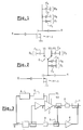
- FIG. 1 there is conventionally shown an RF transistor 1 for amplifying an input signal E having a high average P peak / P ratio.
- the output signal is available at S and the drain bias of the transistor by the voltage Vdrain is provided by a quarter wave line constituting a first decoupling stage D1 comprising a low loss RF capacitor C1 of sufficient value to present a short -circuit, a second decoupling stage D2 comprising a capacitor C2 of higher value than that of C1, capable of supplying current very quickly to transistor 1 during an abrupt rise in power of the signal E and a third decoupling stage D3 comprising a capacitor C3 capable of supplying a strong current for a longer time corresponding to a relatively long power peak consecutive to the presence of low frequency components in the input signal E.
- the capacitors C1, C2, C3 can have respective values of 68 pF, 1000 pF and a few tens of ⁇ F.
- the drain voltage of transistor 1 is provided from two separate supply voltages V1 and V2 respectively, the voltage V2 being greater than the voltage V1.
- This switch 2 makes it possible to apply to the drain of transistor 1, just upstream of the second decoupling stage D2, either the higher (V2) of the two voltages, via the third decoupling stage D3, or the lower (V1) via a fourth decoupling stage D4 comprising a capacitor C4 constituting a long-term charge reservoir ensuring the stability of the drain voltage for a significant period of time.
- the switch 2 is controlled by a control circuit 3 connected to the input E of the amplifier via a signal envelope detection circuit 4.
- the third decoupling stage D3 ensuring the drain a strong current for the time required which can be relatively long, while during the periods off peaks the switch is controlled to apply the lower voltage V1 by replacing stage D3 with the fourth stage D4, which is more appropriate to the situation and capable of ensuring the stability of the drain voltage over a long period which can reach 90% of the time of the amplifier.
- the components 2, C2, C3, C4 constituting all of the decoupling and charge storage stages according to the invention are chosen for their qualities of low inductance and of low internal resistance limiting the parasites generated and are integrated as closely as possible. of transistor 1 in order to ensure very fast and nevertheless clean switching operations.
- the switching system of the invention can be generalized to more than two voltages, with each voltage being associated with a specific decoupling stage, so as to modulate the supply voltage of the amplifier at the rate of l 'envelope of signal E so as to optimize the yield.
- the amplifier requires a high linearity of the output signal S, it is advantageously possible to associate with the device of the invention a correction of the feedforward type which will make it possible to further reduce disturbances such as noise or intermodulation.
- FIG. 3 illustrates such an application of the invention.
- the main amplifier stage receiving at E the input signal and delivering at S the output signal.
- the amplifier stage 1 integrates the decoupling stages D1 to D4 and the switch 2 in FIG. 2 and is connected to the supply voltages V1 and V2.
- the switch 2 integrated in stage 1 ′ is controlled by a control circuit 3 also receiving the input signal E via an envelope detection circuit 4.
- a sample of the signal S is taken at the output of the main amplifier 1 'and compared to the input signal E in a coupler 5.
- the result of this comparison called the error signal, consists of the distortion undergone by the signal and noise introduced by the main amplifier 1 '.
- This error signal is then amplified by a so-called error amplifier 6, its phase is rotated by 180 °, then it is reinjected using a coupler 7 on the main path of the output signal S so as to cancel the distortion. All the delays introduced by the various amplifiers are compensated by delay lines 8 so as to make the cancellation independent of the frequency.
Applications Claiming Priority (2)
| Application Number | Priority Date | Filing Date | Title |
|---|---|---|---|
| FR0213381 | 2002-10-25 | ||
| FR0213381A FR2846489B1 (fr) | 2002-10-25 | 2002-10-25 | Amplificateur de puissance pour systemes de transmission radiofrequences |
Publications (2)
| Publication Number | Publication Date |
|---|---|
| EP1414148A1 true EP1414148A1 (de) | 2004-04-28 |
| EP1414148B1 EP1414148B1 (de) | 2008-08-13 |
Family
ID=32050675
Family Applications (1)
| Application Number | Title | Priority Date | Filing Date |
|---|---|---|---|
| EP03362020A Expired - Lifetime EP1414148B1 (de) | 2002-10-25 | 2003-10-23 | Leistungsverstärker für Hochfrequenz-Transmissionssysteme |
Country Status (4)
| Country | Link |
|---|---|
| EP (1) | EP1414148B1 (de) |
| AT (1) | ATE405028T1 (de) |
| DE (1) | DE60322812D1 (de) |
| FR (1) | FR2846489B1 (de) |
Citations (6)
| Publication number | Priority date | Publication date | Assignee | Title |
|---|---|---|---|---|
| JPS574607A (en) * | 1980-06-11 | 1982-01-11 | Fujitsu Ltd | High-frequency amplifier |
| EP0524772A2 (de) * | 1991-07-23 | 1993-01-27 | Matra Marconi Space UK Limited | Mikrowellenleistungsverstärker |
| EP0673112A1 (de) * | 1994-03-14 | 1995-09-20 | Matsushita Electronics Corporation | Leistungsverstärker und Verfahren dazu |
| US6008698A (en) * | 1998-05-18 | 1999-12-28 | Omnipoint Corporation | Amplifier with dynamically adaptable supply current |
| US20020014920A1 (en) * | 2000-07-14 | 2002-02-07 | Masami Ohnishi | High frequency power amplifier |
| WO2002017478A1 (en) * | 2000-08-24 | 2002-02-28 | Nokia Corporation | Power amplifier arrangement |
-
2002
- 2002-10-25 FR FR0213381A patent/FR2846489B1/fr not_active Expired - Fee Related
-
2003
- 2003-10-23 AT AT03362020T patent/ATE405028T1/de not_active IP Right Cessation
- 2003-10-23 EP EP03362020A patent/EP1414148B1/de not_active Expired - Lifetime
- 2003-10-23 DE DE60322812T patent/DE60322812D1/de not_active Expired - Lifetime
Patent Citations (6)
| Publication number | Priority date | Publication date | Assignee | Title |
|---|---|---|---|---|
| JPS574607A (en) * | 1980-06-11 | 1982-01-11 | Fujitsu Ltd | High-frequency amplifier |
| EP0524772A2 (de) * | 1991-07-23 | 1993-01-27 | Matra Marconi Space UK Limited | Mikrowellenleistungsverstärker |
| EP0673112A1 (de) * | 1994-03-14 | 1995-09-20 | Matsushita Electronics Corporation | Leistungsverstärker und Verfahren dazu |
| US6008698A (en) * | 1998-05-18 | 1999-12-28 | Omnipoint Corporation | Amplifier with dynamically adaptable supply current |
| US20020014920A1 (en) * | 2000-07-14 | 2002-02-07 | Masami Ohnishi | High frequency power amplifier |
| WO2002017478A1 (en) * | 2000-08-24 | 2002-02-28 | Nokia Corporation | Power amplifier arrangement |
Non-Patent Citations (2)
| Title |
|---|
| "The PM2105 Power Amplifier. Application note 2594", 30 June 2000, PACIFIC MONOLITHICS, WWW.RFPOWERNET.COM, XP002241148 * |
| PATENT ABSTRACTS OF JAPAN vol. 006, no. 064 (E - 103) 23 April 1982 (1982-04-23) * |
Also Published As
| Publication number | Publication date |
|---|---|
| EP1414148B1 (de) | 2008-08-13 |
| ATE405028T1 (de) | 2008-08-15 |
| FR2846489A1 (fr) | 2004-04-30 |
| DE60322812D1 (de) | 2008-09-25 |
| FR2846489B1 (fr) | 2005-03-25 |
Similar Documents
| Publication | Publication Date | Title |
|---|---|---|
| EP0283074B1 (de) | Hyperfrequenz-Mischer | |
| FR2816132A1 (fr) | Dispositif reconfigurable pour amplifier des signaux rf | |
| FR2798244A1 (fr) | Circuit et procede d'amplification de puissance a rendement eleve autorisant une large gamme de reduction de puissance dynamique | |
| FR2911019A1 (fr) | Dispositif de linearisation a pre-distortion a amplitude et galbe reglables | |
| FR2558997A1 (fr) | Amplificateur correcteur du temps de propagation de groupe de signaux electriques et chaine d'amplification a frequence intermediaire de faisceaux hertziens comportant un tel amplificateur | |
| FR2770053A1 (fr) | Circuit amplificateur a double gain | |
| EP2339744A1 (de) | Niedrigspannungs-Mischschaltung für eine Übertragungsvorrichtung von UWB-Signalen | |
| FR2826205A1 (fr) | Procede de modulation de l'amplitude d'un signal radiofrequence, et dispositif pour sa mise en oeuvre | |
| EP3381123B1 (de) | Gleichspannungswandlerblock mit mehreren versorgungsspannungen, gleichspannungswandler mit mehreren versorgungsspannungen und zugehöriges hüllkurvennachführungssystem | |
| EP0549043A1 (de) | Integrierte Schaltung mit einem Verstärker mit variabler Verstärkung | |
| EP1414148B1 (de) | Leistungsverstärker für Hochfrequenz-Transmissionssysteme | |
| FR2844066A1 (fr) | Procede de controle des courants de repos d'un dispositif de transposition de frequence du type a conversion directe, et dispositif correspondant | |
| EP2543136B1 (de) | Stromsapnnungswandler mit stromreflektor, eingangsstufe eines verstärkers und entsprechender verstärker | |
| EP0078189B1 (de) | Hyperfrequenter Sender mit hoher Leistung mit Feldeffekttransistoren, insbesondere für Doppler-Radar | |
| EP0060164B1 (de) | Linearer, in gleitendem Klasse A-Betrieb arbeitender Breitbandverstärker mit niedrigem Verbrauch und Schaltung mit wenigstens einem solchen Verstärker | |
| EP2182631A2 (de) | Mikrowellen-Breitband-Verstärkerzelle mit regelbarer Verstärkung und eine solche Zelle umfassender Verstärker | |
| EP0318379A1 (de) | Ultrahochfrequenzverstärker mit sehr breitem Durchlassbereich | |
| EP0201964B1 (de) | Verstärker für Hochfrequenzen | |
| FR2730363A1 (fr) | Amplificateur a gain eleve en hautes frequences et oscillateur a circuit resonant muni d'un tel amplificateur | |
| FR2744304A1 (fr) | Convertisseur numerique-analogique differentiel a fonction de filtrage et compensation de decalage | |
| EP1039652B1 (de) | Antenneanordnung | |
| EP1251634A1 (de) | Transkonduktanzstufe und RF Kommunikationsvorrichtung, die eine solche Stufe umfasst | |
| FR2768277A1 (fr) | Emetteur ayant un rendement de puissance additionnelle ameliore et radio l'employant | |
| FR3048315B1 (fr) | Convertisseur courant-tension, etage d'entree d'un amplificateur et amplificateur correspondant. | |
| FR2890802A1 (fr) | Procede de reduction du niveau d'intermodulation d'ordre 2 d'un transconducteur, et transconducteur correspondant |
Legal Events
| Date | Code | Title | Description |
|---|---|---|---|
| PUAI | Public reference made under article 153(3) epc to a published international application that has entered the european phase |
Free format text: ORIGINAL CODE: 0009012 |
|
| AK | Designated contracting states |
Kind code of ref document: A1 Designated state(s): AT BE BG CH CY CZ DE DK EE ES FI FR GB GR HU IE IT LI LU MC NL PT RO SE SI SK TR |
|
| AX | Request for extension of the european patent |
Extension state: AL LT LV MK |
|
| 17P | Request for examination filed |
Effective date: 20040924 |
|
| AKX | Designation fees paid |
Designated state(s): AT BE BG CH CY CZ DE DK EE ES FI FR GB GR HU IE IT LI LU MC NL PT RO SE SI SK TR |
|
| GRAP | Despatch of communication of intention to grant a patent |
Free format text: ORIGINAL CODE: EPIDOSNIGR1 |
|
| GRAS | Grant fee paid |
Free format text: ORIGINAL CODE: EPIDOSNIGR3 |
|
| GRAA | (expected) grant |
Free format text: ORIGINAL CODE: 0009210 |
|
| AK | Designated contracting states |
Kind code of ref document: B1 Designated state(s): AT BE BG CH CY CZ DE DK EE ES FI FR GB GR HU IE IT LI LU MC NL PT RO SE SI SK TR |
|
| REG | Reference to a national code |
Ref country code: GB Ref legal event code: FG4D Free format text: NOT ENGLISH |
|
| REG | Reference to a national code |
Ref country code: CH Ref legal event code: EP |
|
| REG | Reference to a national code |
Ref country code: IE Ref legal event code: FG4D Free format text: LANGUAGE OF EP DOCUMENT: FRENCH |
|
| REF | Corresponds to: |
Ref document number: 60322812 Country of ref document: DE Date of ref document: 20080925 Kind code of ref document: P |
|
| REG | Reference to a national code |
Ref country code: SE Ref legal event code: TRGR |
|
| PG25 | Lapsed in a contracting state [announced via postgrant information from national office to epo] |
Ref country code: ES Free format text: LAPSE BECAUSE OF FAILURE TO SUBMIT A TRANSLATION OF THE DESCRIPTION OR TO PAY THE FEE WITHIN THE PRESCRIBED TIME-LIMIT Effective date: 20081124 Ref country code: NL Free format text: LAPSE BECAUSE OF FAILURE TO SUBMIT A TRANSLATION OF THE DESCRIPTION OR TO PAY THE FEE WITHIN THE PRESCRIBED TIME-LIMIT Effective date: 20080813 |
|
| PG25 | Lapsed in a contracting state [announced via postgrant information from national office to epo] |
Ref country code: SI Free format text: LAPSE BECAUSE OF FAILURE TO SUBMIT A TRANSLATION OF THE DESCRIPTION OR TO PAY THE FEE WITHIN THE PRESCRIBED TIME-LIMIT Effective date: 20080813 Ref country code: AT Free format text: LAPSE BECAUSE OF FAILURE TO SUBMIT A TRANSLATION OF THE DESCRIPTION OR TO PAY THE FEE WITHIN THE PRESCRIBED TIME-LIMIT Effective date: 20080813 Ref country code: FI Free format text: LAPSE BECAUSE OF FAILURE TO SUBMIT A TRANSLATION OF THE DESCRIPTION OR TO PAY THE FEE WITHIN THE PRESCRIBED TIME-LIMIT Effective date: 20080813 |
|
| REG | Reference to a national code |
Ref country code: IE Ref legal event code: FD4D |
|
| BERE | Be: lapsed |
Owner name: LPA CONCEPTS Effective date: 20081031 |
|
| PG25 | Lapsed in a contracting state [announced via postgrant information from national office to epo] |
Ref country code: DK Free format text: LAPSE BECAUSE OF FAILURE TO SUBMIT A TRANSLATION OF THE DESCRIPTION OR TO PAY THE FEE WITHIN THE PRESCRIBED TIME-LIMIT Effective date: 20080813 Ref country code: BG Free format text: LAPSE BECAUSE OF FAILURE TO SUBMIT A TRANSLATION OF THE DESCRIPTION OR TO PAY THE FEE WITHIN THE PRESCRIBED TIME-LIMIT Effective date: 20081113 Ref country code: IE Free format text: LAPSE BECAUSE OF FAILURE TO SUBMIT A TRANSLATION OF THE DESCRIPTION OR TO PAY THE FEE WITHIN THE PRESCRIBED TIME-LIMIT Effective date: 20080813 |
|
| PG25 | Lapsed in a contracting state [announced via postgrant information from national office to epo] |
Ref country code: MC Free format text: LAPSE BECAUSE OF NON-PAYMENT OF DUE FEES Effective date: 20081031 Ref country code: SK Free format text: LAPSE BECAUSE OF FAILURE TO SUBMIT A TRANSLATION OF THE DESCRIPTION OR TO PAY THE FEE WITHIN THE PRESCRIBED TIME-LIMIT Effective date: 20080813 Ref country code: RO Free format text: LAPSE BECAUSE OF FAILURE TO SUBMIT A TRANSLATION OF THE DESCRIPTION OR TO PAY THE FEE WITHIN THE PRESCRIBED TIME-LIMIT Effective date: 20080813 Ref country code: PT Free format text: LAPSE BECAUSE OF FAILURE TO SUBMIT A TRANSLATION OF THE DESCRIPTION OR TO PAY THE FEE WITHIN THE PRESCRIBED TIME-LIMIT Effective date: 20090113 Ref country code: CZ Free format text: LAPSE BECAUSE OF FAILURE TO SUBMIT A TRANSLATION OF THE DESCRIPTION OR TO PAY THE FEE WITHIN THE PRESCRIBED TIME-LIMIT Effective date: 20080813 |
|
| REG | Reference to a national code |
Ref country code: CH Ref legal event code: PL |
|
| PLBE | No opposition filed within time limit |
Free format text: ORIGINAL CODE: 0009261 |
|
| STAA | Information on the status of an ep patent application or granted ep patent |
Free format text: STATUS: NO OPPOSITION FILED WITHIN TIME LIMIT |
|
| 26N | No opposition filed |
Effective date: 20090514 |
|
| PG25 | Lapsed in a contracting state [announced via postgrant information from national office to epo] |
Ref country code: EE Free format text: LAPSE BECAUSE OF FAILURE TO SUBMIT A TRANSLATION OF THE DESCRIPTION OR TO PAY THE FEE WITHIN THE PRESCRIBED TIME-LIMIT Effective date: 20080813 |
|
| PG25 | Lapsed in a contracting state [announced via postgrant information from national office to epo] |
Ref country code: IT Free format text: LAPSE BECAUSE OF FAILURE TO SUBMIT A TRANSLATION OF THE DESCRIPTION OR TO PAY THE FEE WITHIN THE PRESCRIBED TIME-LIMIT Effective date: 20080813 |
|
| PG25 | Lapsed in a contracting state [announced via postgrant information from national office to epo] |
Ref country code: BE Free format text: LAPSE BECAUSE OF NON-PAYMENT OF DUE FEES Effective date: 20081031 |
|
| PG25 | Lapsed in a contracting state [announced via postgrant information from national office to epo] |
Ref country code: LI Free format text: LAPSE BECAUSE OF NON-PAYMENT OF DUE FEES Effective date: 20081031 Ref country code: CH Free format text: LAPSE BECAUSE OF NON-PAYMENT OF DUE FEES Effective date: 20081031 |
|
| PG25 | Lapsed in a contracting state [announced via postgrant information from national office to epo] |
Ref country code: LU Free format text: LAPSE BECAUSE OF NON-PAYMENT OF DUE FEES Effective date: 20081023 Ref country code: HU Free format text: LAPSE BECAUSE OF FAILURE TO SUBMIT A TRANSLATION OF THE DESCRIPTION OR TO PAY THE FEE WITHIN THE PRESCRIBED TIME-LIMIT Effective date: 20090214 Ref country code: CY Free format text: LAPSE BECAUSE OF FAILURE TO SUBMIT A TRANSLATION OF THE DESCRIPTION OR TO PAY THE FEE WITHIN THE PRESCRIBED TIME-LIMIT Effective date: 20080813 |
|
| PG25 | Lapsed in a contracting state [announced via postgrant information from national office to epo] |
Ref country code: TR Free format text: LAPSE BECAUSE OF FAILURE TO SUBMIT A TRANSLATION OF THE DESCRIPTION OR TO PAY THE FEE WITHIN THE PRESCRIBED TIME-LIMIT Effective date: 20080813 |
|
| PG25 | Lapsed in a contracting state [announced via postgrant information from national office to epo] |
Ref country code: GR Free format text: LAPSE BECAUSE OF FAILURE TO SUBMIT A TRANSLATION OF THE DESCRIPTION OR TO PAY THE FEE WITHIN THE PRESCRIBED TIME-LIMIT Effective date: 20081114 |
|
| REG | Reference to a national code |
Ref country code: FR Ref legal event code: PLFP Year of fee payment: 13 |
|
| REG | Reference to a national code |
Ref country code: FR Ref legal event code: PLFP Year of fee payment: 14 |
|
| PGFP | Annual fee paid to national office [announced via postgrant information from national office to epo] |
Ref country code: FR Payment date: 20161028 Year of fee payment: 14 Ref country code: DE Payment date: 20161024 Year of fee payment: 14 Ref country code: GB Payment date: 20161027 Year of fee payment: 14 |
|
| PGFP | Annual fee paid to national office [announced via postgrant information from national office to epo] |
Ref country code: SE Payment date: 20161027 Year of fee payment: 14 |
|
| REG | Reference to a national code |
Ref country code: DE Ref legal event code: R119 Ref document number: 60322812 Country of ref document: DE |
|
| REG | Reference to a national code |
Ref country code: SE Ref legal event code: EUG |
|
| GBPC | Gb: european patent ceased through non-payment of renewal fee |
Effective date: 20171023 |
|
| REG | Reference to a national code |
Ref country code: FR Ref legal event code: ST Effective date: 20180629 |
|
| PG25 | Lapsed in a contracting state [announced via postgrant information from national office to epo] |
Ref country code: DE Free format text: LAPSE BECAUSE OF NON-PAYMENT OF DUE FEES Effective date: 20180501 Ref country code: GB Free format text: LAPSE BECAUSE OF NON-PAYMENT OF DUE FEES Effective date: 20171023 |
|
| PG25 | Lapsed in a contracting state [announced via postgrant information from national office to epo] |
Ref country code: SE Free format text: LAPSE BECAUSE OF NON-PAYMENT OF DUE FEES Effective date: 20171024 Ref country code: FR Free format text: LAPSE BECAUSE OF NON-PAYMENT OF DUE FEES Effective date: 20171031 |