EP1414010A1 - LCD driver power saving - Google Patents
LCD driver power saving Download PDFInfo
- Publication number
- EP1414010A1 EP1414010A1 EP20020368116 EP02368116A EP1414010A1 EP 1414010 A1 EP1414010 A1 EP 1414010A1 EP 20020368116 EP20020368116 EP 20020368116 EP 02368116 A EP02368116 A EP 02368116A EP 1414010 A1 EP1414010 A1 EP 1414010A1
- Authority
- EP
- European Patent Office
- Prior art keywords
- lcd
- power saving
- backplane
- common
- address
- Prior art date
- Legal status (The legal status is an assumption and is not a legal conclusion. Google has not performed a legal analysis and makes no representation as to the accuracy of the status listed.)
- Withdrawn
Links
- 239000004973 liquid crystal related substance Substances 0.000 claims abstract description 9
- 238000000034 method Methods 0.000 claims description 28
- 238000012360 testing method Methods 0.000 claims description 14
- 238000011156 evaluation Methods 0.000 claims description 9
- 239000011159 matrix material Substances 0.000 description 14
- 238000010586 diagram Methods 0.000 description 11
- 230000003213 activating effect Effects 0.000 description 4
- 240000008042 Zea mays Species 0.000 description 1
- 235000005824 Zea mays ssp. parviglumis Nutrition 0.000 description 1
- 235000002017 Zea mays subsp mays Nutrition 0.000 description 1
- 235000005822 corn Nutrition 0.000 description 1
- 239000010409 thin film Substances 0.000 description 1
- 230000007704 transition Effects 0.000 description 1
Images




Classifications
-
- G—PHYSICS
- G09—EDUCATION; CRYPTOGRAPHY; DISPLAY; ADVERTISING; SEALS
- G09G—ARRANGEMENTS OR CIRCUITS FOR CONTROL OF INDICATING DEVICES USING STATIC MEANS TO PRESENT VARIABLE INFORMATION
- G09G3/00—Control arrangements or circuits, of interest only in connection with visual indicators other than cathode-ray tubes
- G09G3/006—Electronic inspection or testing of displays and display drivers, e.g. of LED or LCD displays
-
- G—PHYSICS
- G09—EDUCATION; CRYPTOGRAPHY; DISPLAY; ADVERTISING; SEALS
- G09G—ARRANGEMENTS OR CIRCUITS FOR CONTROL OF INDICATING DEVICES USING STATIC MEANS TO PRESENT VARIABLE INFORMATION
- G09G2330/00—Aspects of power supply; Aspects of display protection and defect management
- G09G2330/02—Details of power systems and of start or stop of display operation
- G09G2330/021—Power management, e.g. power saving
-
- G—PHYSICS
- G09—EDUCATION; CRYPTOGRAPHY; DISPLAY; ADVERTISING; SEALS
- G09G—ARRANGEMENTS OR CIRCUITS FOR CONTROL OF INDICATING DEVICES USING STATIC MEANS TO PRESENT VARIABLE INFORMATION
- G09G3/00—Control arrangements or circuits, of interest only in connection with visual indicators other than cathode-ray tubes
- G09G3/20—Control arrangements or circuits, of interest only in connection with visual indicators other than cathode-ray tubes for presentation of an assembly of a number of characters, e.g. a page, by composing the assembly by combination of individual elements arranged in a matrix no fixed position being assigned to or needed to be assigned to the individual characters or partial characters
- G09G3/34—Control arrangements or circuits, of interest only in connection with visual indicators other than cathode-ray tubes for presentation of an assembly of a number of characters, e.g. a page, by composing the assembly by combination of individual elements arranged in a matrix no fixed position being assigned to or needed to be assigned to the individual characters or partial characters by control of light from an independent source
- G09G3/36—Control arrangements or circuits, of interest only in connection with visual indicators other than cathode-ray tubes for presentation of an assembly of a number of characters, e.g. a page, by composing the assembly by combination of individual elements arranged in a matrix no fixed position being assigned to or needed to be assigned to the individual characters or partial characters by control of light from an independent source using liquid crystals
- G09G3/3611—Control of matrices with row and column drivers
- G09G3/3622—Control of matrices with row and column drivers using a passive matrix
Definitions
- This invention relates to a method and an apparatus for saving power dissipation during the testing and evaluation of liquid crystal display LCD panels. More particularly this invention relates to the changing of the order of backplane and segment addressing to reduce the power consumed by LCD panels.
- liquid crystal display LCD panels are evaluated by using a checkerboard pattern displayed on the LCD panel as a worst case.
- This checkerboard panel display represents the worst case example for LCD panel power dissipation.
- the checkerboard pattern of LCD panel data 470 is shown in figure 4.
- the ones value is denoted by an 'X' in the LCD cell location 410.
- a zero value is illustrated with a blank square cell area 420 in Fig. 4.
- the LCD panel shown in Figure 4 is an 8 by 8 matrix.
- An even common or 'com' address is also highlighted 440.
- Figure 4 shows the com address 450.
- the com address line selects which row of the matrix in figure 4 is selected for writing to or reading from.
- Figure 4 also shows the segment address 460.
- the segment address would select which column of the LCD panel is being written to or read from.
- a uniquely selected LCD panel cell is selecting by activating the combination of the appropriate segment address and com address in figure 4. For example, cell 420 in Fig. 4 is selected for writing to or reading from by activating com line 1 and segment line 2.
- FIG. 1 shows a conventional prior art block diagram of an LCD panel display subsystem.
- the LCD panel 160 has segment addresses, Seg0, Seg1, Seg2, ... Seg_n 110. These addresses are from the data output of a random access memory 140.
- An address control block 150 produces the read address 120 to the RAM as well as the Common or backplane connections Com0, Com1, Com2, ... Com_n 130.
- the segment address selects the row of the LCD panel matrix while the Com lines select the column of the LCD panel matrix.
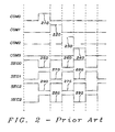
- Figure 2 illustrates the timing diagram for the conventional RAM.
- the common backplane signals Com0, Com1, Com2, and Com3 210, 220.230. 240 occur sequentially every period.
- the timing diagram of the segment population is shown in Fig. 2.
- the column of the matrix is selected when the segment lines are low as we see 250, 290 in figure 2.
- the even columns of the LCD matrix are selected via Seg0 and Seg 2 - 250, 290.
- the odd columns of the LCD matrix are selected via Seg1 and Seg 3 - 270, 285.
- the even columns of the LCD matrix are selected via Seg0 and Seg 2 - 260, 275.
- the odd columns of the LCD matrix are selected via Seg1 and Seg 3 - 280, 295.
- the objects of this invention are achieved by a method that saves power consumption during the testing and evaluation of LCDs.
- the method includes the step of interlacing the access of common or backplane addresses to an LCD.
- the LCD power saving method also includes the interlacing the access of the RAM data driving the LCD segment drivers.
- the LCD power saving method continues with the presenting a common or backplane address to the LCD panel which selects the even common or backplane LCD drivers as a group in time sequence.
- the common or backplane signals are developed from an address control logic block.
- the common or backplane LCD addresses are activated in a time order of com0 first, com1 second, com2 third and com3 fourth.
- the com0, com1, com2 and com3 signals are each active for a period of time, which is the inverse of the frequency required to refresh, said LCD panel.
- the method also includes the presenting of a common or backplane address to the LCD panel which selects the odd common or backplane LCD drivers as a group in time sequence.
- the segment address signals are developed from data read out of a random access memory, RAM.
- the segment address signals are activated such that alternating LCD panel locations are written with ones and zeros in a checkerboard pattern so as to stress the LCD panel in the worst case. This method provides for the saving of power dissipation during testing and evaluation by reducing the amount of segment switching from once every backplane cycle to once every frame.
- the LCD power saving method also saves power consumption during normal operation as well as during testing and evaluation by either interlacing the access of the common or backplane addresses or non-interlacing the access of the common or backplane addresses.
- This method of saving power during normal mode requires the selecting of either interlace or non-interlace modes depending on the content of the LCD display data.
- This normal mode LCD power saving method includes user selection of either interlace or non-interlace modes. This user selection is controlled by a programmable circuit, which senses the content of said display data.
- figure 1 shows the block diagram for the reading and writing of LCD panels.
- the segment address, Seg0-n (110) selects which columns of the LCD panel 160 are being accessed for reading or writing.
- the common or backplane address connections, Com0-3 (130) determine which row of the LCD panel is accessed. These addresses are from the data output of a random access memory 140.
- An address control block 150 produces the read address 120 to the RAM as well as the Common or backplane connections Com0, Com1, Com2, ... Com_n (130).
- Figure 4 illustrates an 8 by 8 LCD panel matrix.
- the LCD panel 470 in figure 4 is loaded with a checkerboard pattern of alternating ones and zeros, which 'X' denotes a one is stored..
- An even common or 'com' address is also highlighted 440.
- Figure 4 shows the com address 450.
- the com address line selects which row of the matrix in figure 4 is selected for writing to or reading from.
- Figure 4 also shows the segment address 460.
- the segment address would select which column of the LCD panel is being written to or read from.
- a uniquely selected LCD panel cell is selecting by activating the combination of the appropriate segment address and com address in figure 4. For example, cell 420 in Fig. 4 is selected for writing to or reading from by activating com line 1 and segment line 2.
- Figure 3 illustrates the timing diagram for the main embodiment of this invention.
- the common backplane signals Com0, Com1, Com2, and Com3 310, 320,330, 340 occur as shown in figure 3.
- the timing diagram of the segment signals is shown in Fig. 3.
- the column of the matrix is selected when the segment lines are low as we see 350, 370 in figure 3.
- the even columns of the LCD matrix are selected via Seg0 and Seg 2 - 350, 370.
- the odd columns of the LCD matrix are selected via Seg1 and Seg 3 - 360, 380.
- Figure 5 shows the prior art case of traditional non-interlaced LCD panel accessing.
- Figure 5 gives the checkerboard data pattern loaded into the LCD panel 510.
- Figure 6b shows the timing diagram of the main embodiment of this invention of the new case of interlaced LCD panel accessing.
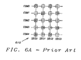
- Figure 6a gives the checkerboard data pattern loaded into the LCD panel 610.
- the advantage of this LCD panel testing invention is the reduction of the total current, Idd drawn, in checkerboard testing mode. This is accomplished by reducing the amount of segment switching from once every backplane cycle to once every once every frame. As seen in figure 5, with the prior art non-interlace method the segment switches every backplane cycle 520. As seen in figure 6b, with the new interlace method the segment switches every frame 620. In addition, figure 6b shows the essence of the interlaced mechanism of this invention. On the plot of Seg1 in figure 6b, the transition from even to odd scan 630 shows that the operation of the segment lines is inverted during the odd frame, which follows the even frame. The segment line is inverted during the odd frame 630, which follows the even frame. Similarly, the Corn signals are inverted during the odd frame which follows the even frame. Another advantage is the the principles of this invention in the testing and evaluating of LCD panels can be used during normal LCD panel operation in the field. This normal mode operation depends on the LCD data patterns.
Landscapes
- Engineering & Computer Science (AREA)
- Physics & Mathematics (AREA)
- Computer Hardware Design (AREA)
- General Physics & Mathematics (AREA)
- Theoretical Computer Science (AREA)
- Control Of Indicators Other Than Cathode Ray Tubes (AREA)
- Liquid Crystal Display Device Control (AREA)
Abstract
Description
- This invention relates to a method and an apparatus for saving power dissipation during the testing and evaluation of liquid crystal display LCD panels. More particularly this invention relates to the changing of the order of backplane and segment addressing to reduce the power consumed by LCD panels.
- Currently, liquid crystal display LCD panels are evaluated by using a checkerboard pattern displayed on the LCD panel as a worst case. This checkerboard panel display represents the worst case example for LCD panel power dissipation. The checkerboard pattern of
LCD panel data 470 is shown in figure 4. The ones value is denoted by an 'X' in theLCD cell location 410. A zero value is illustrated with a blanksquare cell area 420 in Fig. 4. The LCD panel shown in Figure 4 is an 8 by 8 matrix. There are 8 common or backplane addresses shown such as 430 which is an odd common address. An even common or 'com' address is also highlighted 440. Figure 4 shows thecom address 450. The com address line selects which row of the matrix in figure 4 is selected for writing to or reading from. Figure 4 also shows thesegment address 460. The segment address would select which column of the LCD panel is being written to or read from. A uniquely selected LCD panel cell is selecting by activating the combination of the appropriate segment address and com address in figure 4. For example,cell 420 in Fig. 4 is selected for writing to or reading from by activatingcom line 1 andsegment line 2. - Figure 1 shows a conventional prior art block diagram of an LCD panel display subsystem. The
LCD panel 160 has segment addresses, Seg0, Seg1, Seg2, ... Seg_n 110. These addresses are from the data output of arandom access memory 140. Anaddress control block 150 produces theread address 120 to the RAM as well as the Common or backplane connections Com0, Com1, Com2, ... Com_n 130. As we showed in the previous discussion on figure 4, the segment address selects the row of the LCD panel matrix while the Com lines select the column of the LCD panel matrix. - Figure 2 illustrates the timing diagram for the conventional RAM. The common backplane signals Com0, Com1, Com2, and
Com3 210, 220.230. 240 occur sequentially every period. The timing diagram of the segment population is shown in Fig. 2. The column of the matrix is selected when the segment lines are low as we see 250, 290 in figure 2. DuringCom0 time 210, the even columns of the LCD matrix are selected via Seg0 and Seg 2 - 250, 290. During Com1 time 220, the odd columns of the LCD matrix are selected via Seg1 and Seg 3 - 270, 285. During Com2 time, the even columns of the LCD matrix are selected via Seg0 and Seg 2 - 260, 275. DuringCom3 time 240, the odd columns of the LCD matrix are selected via Seg1 and Seg 3 - 280, 295. - U. S. Patent 6,172,661 (Imajo, et al.) "Low power driving method for reducing non-display area of TFT-LCD" describes a low power driving method for reducing non-display area of a thin film transistor liquid crystal display.
- U. S. Patent 6,275,209 (Yamamoto) "LCD driver" describes a liquid crystal display driver.
- U. S. Patent 6,137,465 (Sekine, et al.) "Drive circuit for a LCD device" discloses a drive circuit for a liquid crystal display device.
- It is the objective of this invention to provide a method and an apparatus for saving power dissipation during the testing and evaluation of liquid crystal display LCD panels.
- It is further an object of this invention to the changing of the order of backplane and segment addressing to reduce the power consumed by LCD panels.
- The objects of this invention are achieved by a method that saves power consumption during the testing and evaluation of LCDs. The method includes the step of interlacing the access of common or backplane addresses to an LCD. The LCD power saving method also includes the interlacing the access of the RAM data driving the LCD segment drivers. The LCD power saving method continues with the presenting a common or backplane address to the LCD panel which selects the even common or backplane LCD drivers as a group in time sequence. The common or backplane signals are developed from an address control logic block. The common or backplane LCD addresses are activated in a time order of com0 first, com1 second, com2 third and com3 fourth. The com0, com1, com2 and com3 signals are each active for a period of time, which is the inverse of the frequency required to refresh, said LCD panel. The method also includes the presenting of a common or backplane address to the LCD panel which selects the odd common or backplane LCD drivers as a group in time sequence. The segment address signals are developed from data read out of a random access memory, RAM. The segment address signals are activated such that alternating LCD panel locations are written with ones and zeros in a checkerboard pattern so as to stress the LCD panel in the worst case. This method provides for the saving of power dissipation during testing and evaluation by reducing the amount of segment switching from once every backplane cycle to once every frame.
- The LCD power saving method also saves power consumption during normal operation as well as during testing and evaluation by either interlacing the access of the common or backplane addresses or non-interlacing the access of the common or backplane addresses. This method of saving power during normal mode requires the selecting of either interlace or non-interlace modes depending on the content of the LCD display data. This normal mode LCD power saving method includes user selection of either interlace or non-interlace modes. This user selection is controlled by a programmable circuit, which senses the content of said display data.
-
- FIG. 1 shows a block diagram of an LCD panel system which helps to explain both the prior art and this invention.
- FIG. 2 gives a timing diagram of a prior art LCD panel system.
- FIG. 3 gives a timing diagram of the LCD panel system of this invention.
- FIG. 4 illustrates the checkerboard data pattern that is used to test LCD panels.
- FIG. 5A and 5B illustrate the prior art checkerboard data pattern and non-interlace control signals for LCD panels.
- Fig. 6a illustrates a prior art checkerboard data pattern for testing the LCD.
- FIG. 6b illustrates the interlace timing diagram for the main embodiment of this invention.
- As described previously in the prior art section, figure 1 shows the block diagram for the reading and writing of LCD panels. The segment address, Seg0-n (110) selects which columns of the
LCD panel 160 are being accessed for reading or writing. The common or backplane address connections, Com0-3 (130) determine which row of the LCD panel is accessed. These addresses are from the data output of arandom access memory 140. Anaddress control block 150 produces the readaddress 120 to the RAM as well as the Common or backplane connections Com0, Com1, Com2, ... Com_n (130). - Figure 4 illustrates an 8 by 8 LCD panel matrix. The
LCD panel 470 in figure 4 is loaded with a checkerboard pattern of alternating ones and zeros, which 'X' denotes a one is stored.. There are 8 common or backplane addresses shown such as 430 which is an odd common address. An even common or 'com' address is also highlighted 440. Figure 4 shows thecom address 450. The com address line selects which row of the matrix in figure 4 is selected for writing to or reading from. Figure 4 also shows thesegment address 460. The segment address would select which column of the LCD panel is being written to or read from. A uniquely selected LCD panel cell is selecting by activating the combination of the appropriate segment address and com address in figure 4. For example,cell 420 in Fig. 4 is selected for writing to or reading from by activatingcom line 1 andsegment line 2. - Figure 3 illustrates the timing diagram for the main embodiment of this invention. The common backplane signals Com0, Com1, Com2, and
Com3 310, 320,330, 340 occur as shown in figure 3. The timing diagram of the segment signals is shown in Fig. 3. The column of the matrix is selected when the segment lines are low as we see 350, 370 in figure 3. DuringCom0 310 andCom1 time 330, the even columns of the LCD matrix are selected via Seg0 and Seg 2 - 350, 370. During Com1 time 320 and Com3 time 340, the odd columns of the LCD matrix are selected via Seg1 and Seg 3 - 360, 380. - Figure 5 shows the prior art case of traditional non-interlaced LCD panel accessing. Figure 5 gives the checkerboard data pattern loaded into the
LCD panel 510. - Figure 6b shows the timing diagram of the main embodiment of this invention of the new case of interlaced LCD panel accessing. Figure 6a gives the checkerboard data pattern loaded into the
LCD panel 610. - The advantage of this LCD panel testing invention is the reduction of the total current, Idd drawn, in checkerboard testing mode. This is accomplished by reducing the amount of segment switching from once every backplane cycle to once every once every frame. As seen in figure 5, with the prior art non-interlace method the segment switches every
backplane cycle 520. As seen in figure 6b, with the new interlace method the segment switches everyframe 620. In addition, figure 6b shows the essence of the interlaced mechanism of this invention. On the plot of Seg1 in figure 6b, the transition from even toodd scan 630 shows that the operation of the segment lines is inverted during the odd frame, which follows the even frame. The segment line is inverted during theodd frame 630, which follows the even frame. Similarly, the Corn signals are inverted during the odd frame which follows the even frame. Another advantage is the the principles of this invention in the testing and evaluating of LCD panels can be used during normal LCD panel operation in the field. This normal mode operation depends on the LCD data patterns. - While this invention has been particularly shown and described with Reference to the preferred embodiments thereof, it will be understood by those Skilled in the art that various changes in form and details may be made without Departing from the spirit and scope of this invention.
Claims (26)
- An LCD, liquid crystal display, driver power saving method which saves power consumption during the testing and evaluation of LCDs comprising the steps of:- interlacing the access of common or backplane addresses to a LCD.
- The LCD power saving method of claim 1 further comprising the step of:Interlacing the access of RAM data driving the LCD segment drivers.
- The LCD power saving method of claim 1 further comprising the step of:presenting a common or backplane address to the LCD panel which selects the even common or backplane LCD drivers as a group in time sequence.
- The LCD power saving method of claim 3 wherein the common or backplane signals are developed from an address control logic block.
- The LCD power saving method of claim 3 wherein said common or backplane LCD addresses are activated in a time order of a first address bit (com0), a second address bit (com1), a third address bit (com2) and a fourth address bit (com3).
- The LCD power saving method of claim 5 wherein said first address bit (com0), second address bit (com1), third address bit (com2) and fourth address bit (com3) signals are each active for a period of time which is the inverse of the frequency required to refresh said LCD panel.
- The LCD power saving method of claim 1 further comprising the step of:presenting a common or backplane address to the LCD panel which selects the odd common or backplane LCD drivers as a group in time sequence.
- The LCD power saving method of claim 7 wherein the segment address signals are developed from data read out of a random access memory, RAM.
- The LCD power saving method of claim 7 wherein said segment address signals are activated such that alternating LCD panel locations are written with ones and zeros in a checkerboard pattern so as to stress the LCD panel in the worst case.
- The LCD power saving method of claim 1 wherein power dissipation is saved during testing and evaluation by reducing the amount of segment switching from once every backplane cycle to once every frame.
- An LCD power saving method which saves power consumption during normal operation of the LCD panel comprising the steps of:providing an interlacing mode to the access of the common or backplane addresses, andproviding a non-interlacing mode to the access of the common or backplane addresses.
- The LCD power saving method of claim 11 further comprising the step of:- selecting of said interlace or non-interlace modes depending on the content of the display data.
- The LCD power saving method of claim 12 wherein said user selection of said interlace or non-interlace modes is controlled by a programmable circuit which senses the content of said display data.
- An LCD, liquid crystal display, driver power saving apparatus which saves power consumption during the testing and evaluation of LCDs comprising the means for:- interlacing the access of common or backplane addresses to a LCD.
- The LCD power saving apparatus of claim 14 further comprising the means for:- interlacing the access of RAM data driving the LCD segment drivers.
- The LCD power saving apparatus of claim 14 further comprising the means for:- presenting a common or backplane address to the LCD panelwhich selects the even common or backplane LCD drivers as a group in time sequence.
- The LCD power saving apparatus of claim 16 wherein the common or backplane signals are developed from an address control logic block.
- The LCD power saving apparatus of claim 16 wherein said common or backplane LCD addresses are activated in a time order of a first address bit (com0), a second address bit (com1), a third address bit (com2) and a fourth address bit (com3).
- The LCD power saving apparatus of claim 18 wherein said first address bit (com0), said second address bit (com1), said third address bit (com2) and said fourth address bit (com3) signals are each active for a period of time which is the inverse of the frequency required to refresh said LCD panel.
- The LCD power saving apparatus of claim 14 further comprising the means for:- presenting a common or backplane address to the LCD panel which selects the odd common or backplane LCD drivers as a group in time sequence.
- The LCD power saving apparatus of claim 20 wherein the segment address signals are developed from data read out of a random access memory, RAM.
- The LCD power saving apparatus of claim 20 wherein said segment address signals are activated such that alternating LCD panel locations are written with ones and zeros in a checkerboard pattern so as to stress the LCD panel in the worst case.
- The LCD power saving apparatus of claim 14 wherein power dissipation is saved during testing and evaluation by reducing the amount of segment switching from once every backplane cycle to once every frame.
- An LCD power saving apparatus which saves power consumption during normal operation of the LCD panel comprising the steps of:providing an interlacing mode to access of the common or backplane addresses, andproviding a non-interlacing mode to access of the common or backplane addresses.
- The LCD power saving apparatus of claim 24 further comprising a means for:- selecting of said interlace or non-interlace modes depending on the content of the display data.
- The LCD power saving apparatus of claim 25 wherein said user selection of said interlace or non-interlace modes is controlled by a programmable circuit which senses the content of said display data
Priority Applications (2)
| Application Number | Priority Date | Filing Date | Title |
|---|---|---|---|
| EP20020368116 EP1414010A1 (en) | 2002-10-24 | 2002-10-24 | LCD driver power saving |
| US10/290,129 US7256777B2 (en) | 2002-10-24 | 2002-11-07 | LCD driver power saving during evaluation |
Applications Claiming Priority (1)
| Application Number | Priority Date | Filing Date | Title |
|---|---|---|---|
| EP20020368116 EP1414010A1 (en) | 2002-10-24 | 2002-10-24 | LCD driver power saving |
Publications (1)
| Publication Number | Publication Date |
|---|---|
| EP1414010A1 true EP1414010A1 (en) | 2004-04-28 |
Family
ID=32050137
Family Applications (1)
| Application Number | Title | Priority Date | Filing Date |
|---|---|---|---|
| EP20020368116 Withdrawn EP1414010A1 (en) | 2002-10-24 | 2002-10-24 | LCD driver power saving |
Country Status (2)
| Country | Link |
|---|---|
| US (1) | US7256777B2 (en) |
| EP (1) | EP1414010A1 (en) |
Families Citing this family (4)
| Publication number | Priority date | Publication date | Assignee | Title |
|---|---|---|---|---|
| KR100515318B1 (en) * | 2003-07-30 | 2005-09-15 | 삼성에스디아이 주식회사 | Display and driving method thereof |
| KR100620519B1 (en) * | 2004-02-16 | 2006-09-13 | 비오이 하이디스 테크놀로지 주식회사 | Interlacing video signal compensation method and apparatus |
| WO2010123620A1 (en) * | 2009-04-24 | 2010-10-28 | Arizona Board of Regents, a body corporate acting for and on behalf of Arizona State University | Methods and system for electrostatic discharge protection of thin-film transistor backplane arrays |
| CN113899967A (en) * | 2021-09-08 | 2022-01-07 | 信利半导体有限公司 | Method and system for testing serial leakage pen of liquid crystal display screen |
Citations (3)
| Publication number | Priority date | Publication date | Assignee | Title |
|---|---|---|---|---|
| EP0945844A2 (en) * | 1998-03-26 | 1999-09-29 | Fujitsu Limited | Display and method of driving the display |
| WO2001082284A1 (en) * | 2000-04-26 | 2001-11-01 | Ultrachip, Inc. | Low power lcd driving scheme |
| US20020075217A1 (en) * | 2000-11-02 | 2002-06-20 | Masafumi Hoshino | Method of driving liquid crystal display panel |
Family Cites Families (5)
| Publication number | Priority date | Publication date | Assignee | Title |
|---|---|---|---|---|
| TW275684B (en) | 1994-07-08 | 1996-05-11 | Hitachi Seisakusyo Kk | |
| JP3554135B2 (en) * | 1997-04-24 | 2004-08-18 | ローム株式会社 | LCD driver |
| JP3024618B2 (en) | 1997-11-19 | 2000-03-21 | 日本電気株式会社 | LCD drive circuit |
| US7362294B2 (en) * | 2000-04-26 | 2008-04-22 | Jps Group Holdings, Ltd | Low power LCD with gray shade driving scheme |
| US7375760B2 (en) * | 2001-12-31 | 2008-05-20 | Texas Instruments Incorporated | Content-dependent scan rate converter with adaptive noise reduction |
-
2002
- 2002-10-24 EP EP20020368116 patent/EP1414010A1/en not_active Withdrawn
- 2002-11-07 US US10/290,129 patent/US7256777B2/en not_active Expired - Lifetime
Patent Citations (3)
| Publication number | Priority date | Publication date | Assignee | Title |
|---|---|---|---|---|
| EP0945844A2 (en) * | 1998-03-26 | 1999-09-29 | Fujitsu Limited | Display and method of driving the display |
| WO2001082284A1 (en) * | 2000-04-26 | 2001-11-01 | Ultrachip, Inc. | Low power lcd driving scheme |
| US20020075217A1 (en) * | 2000-11-02 | 2002-06-20 | Masafumi Hoshino | Method of driving liquid crystal display panel |
Also Published As
| Publication number | Publication date |
|---|---|
| US7256777B2 (en) | 2007-08-14 |
| US20040080503A1 (en) | 2004-04-29 |
Similar Documents
| Publication | Publication Date | Title |
|---|---|---|
| JP3253481B2 (en) | Memory interface circuit | |
| JP3588802B2 (en) | Electro-optical device and driving method thereof, liquid crystal display device and driving method thereof, driving circuit of electro-optical device, and electronic apparatus | |
| CN100356433C (en) | Driving method for display, display and electronic device | |
| US6040826A (en) | Driving circuit for driving simple matrix type display apparatus | |
| US20020109653A1 (en) | Liquid crystal driver circuit and liquid crystal display device | |
| JP3428593B2 (en) | Display device and driving method thereof | |
| US20030085858A1 (en) | Cholesteric liquid crystal display device and display driver | |
| JPWO1996016346A1 (en) | Display device, display device driving method, and electronic device | |
| JPWO1999040561A1 (en) | Electro-optical device and driving method thereof, liquid crystal display device and driving method thereof, driving circuit for electro-optical device, and electronic device | |
| JPH10105085A (en) | Liquid crystal display device and driving method thereof | |
| JP2002156954A (en) | Liquid crystal display | |
| US8421807B2 (en) | Display device | |
| US7969427B2 (en) | Control device for display panel and display apparatus having same | |
| US20100026617A1 (en) | Method and device for activating scan lines of a passive matrix liquid crystal display (lcd) panel | |
| CN119360796A (en) | Display panel, driving method thereof, driving circuit and display device | |
| US20040080503A1 (en) | LCD driver power saving during evaluation | |
| US6870531B2 (en) | Circuit and method for controlling frame ratio of LCD and LCD system having the same | |
| JP2002156953A (en) | Display device and driving method thereof | |
| JPH09197377A (en) | Liquid crystal driving method and liquid crystal driving device | |
| JP3633455B2 (en) | Drive device incorporating storage device, electro-optical device using the drive device, and electronic apparatus | |
| JP3632697B2 (en) | Liquid crystal display device, driving method thereof, and electronic apparatus | |
| JP3318667B2 (en) | Liquid crystal display | |
| JP3578164B2 (en) | Electro-optical device, driving circuit of electro-optical device, and electronic apparatus | |
| JP2001125071A (en) | Electro-optical device and driving method thereof, liquid crystal display device and driving method thereof, driving circuit of electro-optical device, and electronic apparatus | |
| US8068081B2 (en) | Driver for driving display panel and method for reading/writing in memory thereof and thin film transistor liquid crystal display using the same |
Legal Events
| Date | Code | Title | Description |
|---|---|---|---|
| PUAI | Public reference made under article 153(3) epc to a published international application that has entered the european phase |
Free format text: ORIGINAL CODE: 0009012 |
|
| AK | Designated contracting states |
Kind code of ref document: A1 Designated state(s): AT BE BG CH CY CZ DE DK EE ES FI FR GB GR IE IT LI LU MC NL PT SE SK TR |
|
| AX | Request for extension of the european patent |
Extension state: AL LT LV MK RO SI |
|
| 17P | Request for examination filed |
Effective date: 20041025 |
|
| AKX | Designation fees paid |
Designated state(s): AT BE BG CH CY CZ DE DK EE ES FI FR GB GR IE IT LI LU MC NL PT SE SK TR |
|
| APBN | Date of receipt of notice of appeal recorded |
Free format text: ORIGINAL CODE: EPIDOSNNOA2E |
|
| APBR | Date of receipt of statement of grounds of appeal recorded |
Free format text: ORIGINAL CODE: EPIDOSNNOA3E |
|
| APAF | Appeal reference modified |
Free format text: ORIGINAL CODE: EPIDOSCREFNE |
|
| APAF | Appeal reference modified |
Free format text: ORIGINAL CODE: EPIDOSCREFNE |
|
| APBT | Appeal procedure closed |
Free format text: ORIGINAL CODE: EPIDOSNNOA9E |
|
| STAA | Information on the status of an ep patent application or granted ep patent |
Free format text: STATUS: THE APPLICATION IS DEEMED TO BE WITHDRAWN |
|
| 18D | Application deemed to be withdrawn |
Effective date: 20130502 |