EP1412940B1 - Verfahren und vorrichtung zum betreiben eines zeitkontinuierlichen filters eines lese-/schreibkanals für ein festplattenlaufwerk - Google Patents
Verfahren und vorrichtung zum betreiben eines zeitkontinuierlichen filters eines lese-/schreibkanals für ein festplattenlaufwerk Download PDFInfo
- Publication number
- EP1412940B1 EP1412940B1 EP02737115A EP02737115A EP1412940B1 EP 1412940 B1 EP1412940 B1 EP 1412940B1 EP 02737115 A EP02737115 A EP 02737115A EP 02737115 A EP02737115 A EP 02737115A EP 1412940 B1 EP1412940 B1 EP 1412940B1
- Authority
- EP
- European Patent Office
- Prior art keywords
- filter
- read
- servo
- signal
- continuous time
- Prior art date
- Legal status (The legal status is an assumption and is not a legal conclusion. Google has not performed a legal analysis and makes no representation as to the accuracy of the status listed.)
- Expired - Lifetime
Links
- 238000000034 method Methods 0.000 title claims description 19
- 238000001914 filtration Methods 0.000 claims description 10
- 238000012546 transfer Methods 0.000 claims description 6
- 230000001419 dependent effect Effects 0.000 claims description 4
- 230000004907 flux Effects 0.000 description 12
- 238000005516 engineering process Methods 0.000 description 8
- 230000008569 process Effects 0.000 description 7
- 238000010586 diagram Methods 0.000 description 6
- 238000012545 processing Methods 0.000 description 6
- 238000001514 detection method Methods 0.000 description 5
- 230000004044 response Effects 0.000 description 4
- 238000007476 Maximum Likelihood Methods 0.000 description 3
- 238000012937 correction Methods 0.000 description 3
- 238000004519 manufacturing process Methods 0.000 description 3
- 238000011084 recovery Methods 0.000 description 3
- 239000003990 capacitor Substances 0.000 description 2
- 238000013500 data storage Methods 0.000 description 2
- 238000012986 modification Methods 0.000 description 2
- 230000004048 modification Effects 0.000 description 2
- 230000002238 attenuated effect Effects 0.000 description 1
- 230000008859 change Effects 0.000 description 1
- 238000004891 communication Methods 0.000 description 1
- 230000000295 complement effect Effects 0.000 description 1
- 230000003247 decreasing effect Effects 0.000 description 1
- 238000013461 design Methods 0.000 description 1
- 230000005672 electromagnetic field Effects 0.000 description 1
- 239000002184 metal Substances 0.000 description 1
- 229910044991 metal oxide Inorganic materials 0.000 description 1
- 150000004706 metal oxides Chemical class 0.000 description 1
- 229910021420 polycrystalline silicon Inorganic materials 0.000 description 1
- 229920005591 polysilicon Polymers 0.000 description 1
- 230000035755 proliferation Effects 0.000 description 1
- 230000009467 reduction Effects 0.000 description 1
- 239000004065 semiconductor Substances 0.000 description 1
- 230000035945 sensitivity Effects 0.000 description 1
Images


Classifications
-
- G—PHYSICS
- G11—INFORMATION STORAGE
- G11B—INFORMATION STORAGE BASED ON RELATIVE MOVEMENT BETWEEN RECORD CARRIER AND TRANSDUCER
- G11B20/00—Signal processing not specific to the method of recording or reproducing; Circuits therefor
- G11B20/10—Digital recording or reproducing
- G11B20/14—Digital recording or reproducing using self-clocking codes
- G11B20/1403—Digital recording or reproducing using self-clocking codes characterised by the use of two levels
- G11B20/1423—Code representation depending on subsequent bits, e.g. delay modulation, double density code, Miller code
- G11B20/1426—Code representation depending on subsequent bits, e.g. delay modulation, double density code, Miller code conversion to or from block codes or representations thereof
-
- G—PHYSICS
- G11—INFORMATION STORAGE
- G11B—INFORMATION STORAGE BASED ON RELATIVE MOVEMENT BETWEEN RECORD CARRIER AND TRANSDUCER
- G11B20/00—Signal processing not specific to the method of recording or reproducing; Circuits therefor
- G11B20/10—Digital recording or reproducing
- G11B20/10009—Improvement or modification of read or write signals
Definitions
- Computer hard disk drives also known as fixed disk drives or hard drives, have become a de facto standard data storage component of modem computer systems and are making further inroads into modem consumer electronics as well. Their proliferation can be directly attributed to their low cost, high storage capacity and high reliability, in addition to wide availability, low power consumption, high data transfer speeds and decreasing physical size.
- These disk drives typically consist of one or more rotating magnetic platters encased within an environmentally controlled housing that further includes all of the electronics and mechanics to read and write data and interface with other devices.
- Read/write heads are positioned above each of the platters, and typically on each face, to record and read data.
- the electronics of a hard disk drive are coupled with these read/write heads and include numerous components to control the position of the heads and generate or sense the electromagnetic fields representing data. These components receive data from a host device, such as a personal computer, and translate that data into magnetic encodings written onto the disk platters by the heads.
- the electronics locate the desired data, sense the magnetic encodings which represent that data and translate those encodings back into the binary digital information which the host device can understand. Further, error detection and correction algorithms are applied to ensure accurate storage and retrieval of data.
- the read/write head of which a typical hard disk has several, is the interface between magnetic platters and the disk drive electronics.
- the read/write head actually reads and writes the magnetically encoded data as areas of magnetic flux on the platters.
- Data consisting of binary 1's and 0's, are encoded by sequences of the presence or absence of flux reversals recorded or detected by the read/write head.
- a flux reversal is a change in the magnetic flux in two contiguous areas of the disk platter.
- PRML Partial Response Maximum Likelihood
- PRML-based drives digitally sample this analog waveform (the "Partial Response") and use advanced signal processing technologies to determine the bit pattern represented by that wave form (the “Maximum Likelihood”).
- This technology in conjunction magneto-resistive (“MR”) heads, have permitted manufacturers to further increase data storage densities. PRML technology further tolerates more noise in the sensed magnetic signals permitting the use of lower quality platters and read/write heads which increases manufacturing yields and lowers costs.
- hard disk drives are typically differentiated by factors such as cost/megabyte of storage, data transfer rate, power requirements and form factor (physical dimensions) with the bulk of competition based on cost.
- factors such as cost/megabyte of storage, data transfer rate, power requirements and form factor (physical dimensions) with the bulk of competition based on cost.
- the continuous time filter is adapted to receive an analog signal and includes an input multiplexer and an output multiplexer.
- the input multiplexer receives the analog signal and transmits the analog signal to a read filter circuit when the continuous time filter is in read mode and to a servo filter circuit when the continuous time filter is in servo mode.
- the output multiplexer receives a read filter output signal from the read filter circuit when the continuous time filter is in read mode and receives a servo filter output signal from the servo filter circuit when the continuous time filter is in servo mode.
- the preferred embodiments further relate to a method for operating a continuous time filter of a read/write channel for a hard disk drive.
- the method includes receiving an analog signal by an input multiplexer and routing the analog signal to a read filter circuit when the continuous time filter is in read mode and routing the analog signal to a servo filter circuit when the continuous time filter is in servo mode.
- the method further includes filtering the analog signal using a read filter circuit when the continuous time filter is in read mode and filtering the analog signal using a servo filter circuit when the continuous time filter is in servo mode.
- the method includes generating a read filter output signal when the continuous time filter is in read mode and generating a servo filter output signal when the continuous time filter is in servo mode.
- the embodiments described herein relate to a PRML-based read/write channel device for hard disk drive controllers.
- the read/write channel is a device coupled with the read/write heads of the hard disk drive.
- the phrase "coupled with” is defined to mean directly connected to or indirectly connected with through one or more intermediate components. Such intermediate components may include both hardware and software based components.
- the read/write channel converts binary/digital data from the host device into the electrical impulses which drive the read/write head to magnetically record the data to the disk drive platters. Further, the read/write channel receives the analog waveform magnetically sensed by the read/write heads and converts that waveform back into the binary/digital data stored on the drive.
- FIG. 1A there is shown a block diagram of an exemplary hard disk drive 100 coupled with a host device 112. For clarity, some components, such as the servo/actuator motor control, are not shown.
- the drive 100 includes the magnetic platters and spindle motor 102, the read/write heads and actuator assembly 104, pre-amplifiers 106, a read/write channel 108 and a controller 110.
- the pre-amplifiers 106 are coupled with the read/write channel 108 via interfaces 114, 116.
- the controller 110 interfaces with the read/write channel 108 via interfaces 118, 120.
- the host device 112 For reads from the hard disk 100, the host device 112 provides a location identifier which identifies the location of the data on the disk drive, e.g. a cylinder and sector address.
- the controller 110 receives this address and determines the physical location of the data on the platters 102.
- the controller 110 then moves the read/write heads into the proper position for the data to spin underneath the read/write heads 104.
- the read/write head 104 senses the presence or absence of flux reversals, generating a stream of analog signal data. This data is passed to the pre-amplifiers 106 which amplifies the signal and passes it to the read/write channel 108 via the interface 114.
- the read/write channel receives the amplified analog waveform from the pre-amplifiers 106 and decodes this waveform into the digital binary data that it represents. This digital binary data is then passed to the controller 110 via the interface 118.
- the controller 110 interfaces the hard drive 100 with the host device 112 and may contain additional functionality, such as caching or error detection/correction functionality, intended to increase the operating speed and/or reliability of the hard drive 100.
- the host device 112 provides the controller 110 with the binary digital data to be written and the location, e.g. cylinder and sector address, of where to write it.
- the controller 110 moves the read/write heads 104 to the proper location and sends the binary digital data to be written to the read/write channel 108 via interface 120.
- the read/write channel 108 receives the binary digital data, encodes it and generates analog signals which are used to drive the read/write head 104 to impart the proper magnetic flux reversals onto the magnetic platters 102 representing the binary digital data.
- the generated signals are passed to the pre-amplifiers 106 via interface 116 which drive the read/write heads 104.
- CMOS complementary metal oxide semiconductor
- PRML Partial Response Maximum Likelihood
- the read/write channel 108 is implemented as an integrated circuit using a complementary metal oxide semiconductor (“CMOS") process at 0.18 micron.
- CMOS processes include processes which use metal gates as well as polysilicon gates.
- CMOS processes include processes which use metal gates as well as polysilicon gates.
- other process technologies and feature sizes may be used and that the circuitry disclosed herein may be further integrated with other circuitry comprising the hard disk electronics such as the hard disk controller logic.
- the read/write channel 108 converts between binary digital information and the analog signals representing the magnetic flux on the platters 102.
- the read/write channel 108 is divided into two main sections, the read path 156 and the write path 158.
- the write path 158 includes a parallel-to-serial converter 144, a run-length-limited (“RLL") encoder 146, a parity encoder 148, a write pre-compensation circuit 150 and a driver circuit 152.
- the parallel-to-serial converter 144 receives data from the host device 112 via interface 120 eight bits at a time.
- the converter 144 serializes the input data and sends the serial bit stream to the RLL encoder 146.
- the RLL encoder 146 encodes the serial bit stream into symbolic binary sequences according to a known run-length limited algorithm for recording on the platters 102.
- the exemplary RLL encoder uses a 32/33 bit symbol code to ensure that flux reversals are properly spaced and that long runs of data without flux reversals are not recorded.
- the RLL encoded data is then passed to the parity encoder 148 which adds a parity bit to the data.
- odd parity is used to ensure that long run's of 0's and 1's are not recorded due to the magnetic properties of such recorded data.
- the parity encoded data is subsequently treated as an analog signal rather than a digital signal.
- the analog signal is passed to a write pre-compensation circuit 150 which dynamically adjusts the pulse widths of the bit stream to account for magnetic distortions in the recording process.
- the adjusted analog signal is passed to a driver circuit 152 which drives the signal to the pre-amplifiers 106 via interface 116 to drive the read/write heads 104 and record the data.
- the exemplary driver circuit 152 includes a pseudo emitter coupled logic (“PECL”) driver circuit which generates a differential output to the pre-amplifiers 106.
- PECL pseudo emitter coupled logic
- the read path 156 includes an attenuation circuit/input resistance 122, a variable gain amplifier (“VGA”) 124, a magneto-resistive asymmetry linearizer (“MRA”) 126, a continuous time filter (“CTF”) 128, a buffer 130, an analog to digital converter (“ADC”) 132, a finite impulse response (“FIR”) filter 134, an interpolated timing recovery (“ITR”) circuit 136, a Viterbi algorithm detector 138, a parity decoder 140 and a run-length-limited (“RLL”) decoder 142.
- VGA variable gain amplifier
- MRA magneto-resistive asymmetry linearizer
- CTF continuous time filter
- ADC analog to digital converter
- FIR finite impulse response
- ITR interpolated timing recovery
- the amplified magnetic signals sensed from the platters 102 by the read/write head 104 are received by the read/write channel 108 via interface 114.
- the analog signal waveform representing the sensed magnetic signals is first passed through an input resistance 122 which is a switching circuit to attenuate the signal and account for any input resistance.
- the attenuated signal is then passed to a VGA 124 which amplifies the signal.
- the amplified signal is then passed to the MRA 126 which adjusts the signal for any distortion created by the recording process. Essentially, the MRA 126 performs the opposite function of the write-pre-compensation circuit 150 in the write path 158.
- the signal is next passed through the CTF 128, which is essentially a low pass filter, to filter out noise.
- the filtered signal is then passed to the ADC 132 via the buffer 130 which samples the analog signal and converts it to a digital form.
- the digital signal is then passed to a FIR filter 134 and then to a timing recovery circuit 136.
- the timing recovery circuit 136 is connected (not shown in the figure) to the FIR filter 134, the MRA 126 and the VGA 124 in a feedback orientation to adjust these circuits according to the signals received to provide timing compensation.
- the exemplary FIR filter 134 is a 10 tap FIR filter.
- the digital signal is then passed to the Viterbi algorithm detector 138 which determines the binary bit pattern represented by the digital signal using digital signal processing techniques.
- the exemplary Viterbi algorithm detector 138 uses a 32 state Viterbi processor.
- the binary data represented by the digital signal is then passed to the parity decoder 140 which removes the parity bit and then to the RLL decoder 142 which decodes the binary RLL encoding symbols back into the actual binary data that they represents This data is then passed to the controller 110 via the interface 118.
- the read/write channel 108 further includes a clock synthesizer 154.
- the clock synthesizer 154 generates the clock signals required for operating the read/write channel 108.
- the exemplary clock synthesizer 154 includes a phased lock look (“PLL”) (not shown) with a voltage controlled oscillator and various clock dividers to generate the necessary frequencies.
- PLL phased lock look
- the read/write channel 108 of the hard drive 100 operates in two different modes: a read mode and a servo mode.
- Controller 110 sends a read gate signal 216 and a servo gate signal 218 to the continuous time filter 128 via interface 120, as illustrated in Figure 1A and Figure 2.
- the read gate signal 216 instructs the continuous time filter 128, to go into read mode, while the servo gate signal 218 instruct the continuous time filter 128, to go into servo mode.
- the hard drive 100 reads data stored on the magnetic platters 102.
- the hard drive 100 tries to figure out the absolute position of the read/write head 104 using servo wedges located on the magnetic platters 102.
- the hard drive 100 insures that there is no misalignment of the read/write head 104.
- the continuous time filter 128 alternates between the read mode and the servo mode.
- the time required to alternate between the read mode and the servo mode is referred to herein as switching time.
- the switching time sets a limit on the size of a gap located on the magnetic platters 102 between a read gate and a servo gate or between the servo gate and the read gate.
- the continuous time filter 128 includes filtering circuitry that needs to be calibrated before operation of the continuous time filter 128 can begin.
- the amount of time required to calibrate the filtering circuitry can increase the switching time, and thus increase the size of the gap.
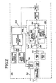
- the continuous time filter 128 includes a separate read filter circuit 254 and a separate servo filter circuit 256 in order to reduce the switching time, as illustrated in Figure 2.
- the continuous time filter 128 is able to calibrate the read filter circuit 254 while the servo filter circuit 256 is in operation, and conversely the continuous time filter 128 is also able to calibrate the servo filter circuit 256 while the read filter circuit 254 is in operation, thus allowing for a reduction in the amount of time required to switch from the read mode to the servo mode, and from the servo mode back to the read mode.
- the limit on the size of the gap between the read gate and the servo gate or between the servo gate and the read gate can be reduced.
- the limit on the size of the gap is reduced from 8 bytes to less than two bytes, and more preferably, to less than one byte.
- the continuous time filter 128 also includes an input multiplexer 220 and an output multiplexer 222.
- the input multiplexer 220 receives an analog signal 215 from the MRA 126 and transmits the analog signal 215 to either the read filter circuit 254 or the servo filter circuit 256, depending on whether the continuous time filter 128 is in read mode or in servo mode. More specifically, if the controller 110 sends a read gate signal 216 through interface 120 to the continuous time filter 128, the continuous time filter 128 is in read mode. If the controller 110 sends a servo gate signal 218 through interface 120 to the continuous time filter 128, the continuous time filter 128 is in servo mode.
- the read gate signal 216 is also received by the input multiplexer 220.
- a gate 217 within the input multiplexer 220 is turned on and the analog signal 215 is directed to the read filter circuit 254, and more specifically, a read filter 224, for processing.
- the read filter 224 Upon processing the analog signal 215, the read filter 224 generates a read filter output signal 225 that is then passed on to the output multiplexer 222.
- the output multiplexer 222 also receives a portion of the read gate signal 216.
- a gate 221 within the output multiplexer 222 is turned on and the read filter output signal 225 is directed to the buffer 130, as illustrated in Figures 2 and 3.
- the servo gate signal 218 is also received by the input multiplexer 220.
- the servo gate signal 218, that is, when the servo gate signal 218 is high, a gate 219 within the input multiplexer 220 is turned on and the analog signal 215 diverted to the servo filter circuit 256, and more specifically, a servo filter 226, for processing.
- the servo filter 224 Upon processing the analog signal 215, the servo filter 224 generates a servo filter output signal 227 that is then passed on to the output multiplexer 222.
- the output multiplexer 222 also receives a portion of the servo gate signal 218.
- a gate 223 within the output multiplexer 222 is turned on and the servo filter output signal 227 is directed to the buffer 130, as illustrated in Figures 2 and 3.
- the input multiplexer 220 receive the analog signal 215 from a stemming node 154.
- the stemming node 154 is connected with an offset correction DAC (ODAC) 160.
- ODAC 160 introduces an analog offset, which is proportional to a digital input controlled by a DC-restore-loop.
- the DC-restore-loop decides based on the output from the ADC 132 if the offset value of the analog offset introduced by the ODAC 160 has to be increased or reduced.
- the goal of the DC-restore-loop is to remove any effective offset in the analog signal path.
- the analog signal path is the signal path that begins with the signal input to the VGA 124 and ends with the ADC 132.
- the DC-restore-loop increases or reduces the value of the analog offset introduced by the ODAC 160 by adding an offset to the analog signal at the output of MRA 126.
- the analog offset introduced by the ODAC 160 has exactly the same absolute value as the effective offset in the analog signal path.
- the sign of the analog offset introduced by the ODAC 160 is opposite from the sign of the effective offset in the analog signal path. In this way, the DC-restore-loop cancels the effective offset in the analog signal path.
- the continuous time filter 128 also receives a read/write clock signal 206 and a servo clock signal 202, as illustrated in Figure 2.
- a read/write clock generator 204 generates the read/write clock signal 206 and a servo clock generator 200 generates the servo clock signal 202, as illustrated in Figure 2.
- the read/write clock signal 206 and the servo clock signal 202 are also sent to a clock multiplexer 208.
- the clock multiplexer 208 then allows either the read/write clock signal 206 or the servo clock signal 202, depending on whether the read write channel 108 is in read mode or in servo mode, to pass through the clock multiplexer 208 and pass to both the ADC 132 and a view DAC 212, as illustrated in Figure 2.
- the view DAC 212 also receives a 7 bit view DAC data from another portion of the read/write channel 108 and generates a view DAC output signal 214.
- the read filter circuit 254 includes a divider 228, a resistor capacitor (RC) filter 230, a limiter 232, a level shifter 234, an inverter 236, an NMOS device 237, a phase detector 238, a charge pump 244, a loop filter 246, and a read filter (RCTF) 224.
- RC resistor capacitor
- the divider 228, the RC filter 230, the limiter 232, the level shifter 234, the inverter 236, and the NMOS device 237 form a calibration signal generator circuit designed to generate a calibration signal 241 used to calibrate the read filter 224.
- the divider 228 receives the read/write clock signal 206, having a set frequency, from the read/write clock generator 204. While in this embodiment, the divider 228 receives the read/write clock signal 206, the divider 228 may receive a clock signal generated by an alternate clock generator. The divider 228 divides the frequency of the read/write clock signal 206 by a fixed multiple to generate a divided signal 229.
- the divider 228 may receive a read/write clock signal 206 having a frequency of 800 MHz and divide that signal by 4 to produce a divided signal 229 having a frequency of 200 MHz.
- the divider 228 sends the divided signal 229 to the RC filter 230 which slows the rise and fall time of the divided signal 229 so that the divided signal 229 has a "softer" appearance.
- the RC filter 230 then sends the resultant signal to the limiter 232 which then reduces the strength of the signal by essentially reducing the voltage of the signal to produce a voltage limited signal 233.
- the voltage limited signal 233 then is sent to the level shifter 234 which offsets the value of the voltage limited signal 233 by adding or subtracting a fixed amount of voltage to the voltage limited signal 233, thus creating a calibration signal 241.
- the calibration signal 241 is sent to the NMOS device 237.
- the inverter 236 receives the read gate signal 216.
- the inverter 236 inverts the read gate signal 216 and creates an inverted signal 239.
- the inverted signal 239 is then sent to the NMOS device 237 and the charge pump 244.
- the NMOS device 237 has a gate that is controlled by the inverted signal 239. For example, in one preferred embodiment, if the value of the read gate signal 216 is high, the value of the inverted signal 239 is low, and therefore the gate within the NMOS device 237 is turned off and the NMOS device 237 does not allow the calibration signal 241 to pass through to the phase detector 238 and the read filter 224. Additionally, if the value of the read gate signal 216 is high, the value of the inverted signal 239 is low, and therefore the charge pump 244 is disabled, so that regardless of the outputs of the phase detector 238, the charge pump 244 does not generate any current output.
- the NMOS device 237 is used to control whether or not the calibration signal 241 is allowed to pass to the phase detector 238 and the read filter 224, other devices known to those skilled in the art may be used.
- the calibration signal 241 has been generated in order to calibrate the read filter 224. If the read gate signal 216 is low, the gate within the NMOS device 237 turns on and allows the calibration signal 241 to pass through to the phase detector 238 and the read filter 224. Additionally, if the read gate signal 216 is low, that is, if the read gate signal 216 is not received, the gate 217 of the input multiplexer 220 is turned off and does not allow the analog signal 215 to pass through to the read filter 224. However, if the read gate signal 216 is high, the gate within the NMOS device 237 turns off and does not allow the calibration signal 241 to pass through to the phase detector 238 and the read filter 224.
- the gate 217 of the input multiplexer 220 is turned on and allows the analog signal 215 to pass through to the read filter 224.
- the read filter 224 is calibrated, and when the read gate signal 216 is high, the read filter 224 immediately receives and filters the analog signal 215 without having to wait.
- the switching time for the continuous time filter 128 is reduced.
- the phase detector 238, the charge pump 244, and the loop filter 246 form a read filter calibration circuit.
- the goal of the read filter calibration circuit is to calibrate and tune the cut off frequency of read filter 224 to a value, which is related to the value of the read/write clock signal 206. This is done in such a way that the calibration signal 241 input into the read filter 224 and the signal output from the read filter 224, a read filter output signal 225, have the same phase. If the read gate signal 216 is low signal, the calibration signal 241 passes through the NMOS device 237 and enters the phase detector 238 and the read filter 224, as illustrated in Figure 3.
- the phase detector 238 receives the calibration signal 241 and compares the phase of the calibration signal 241 with the phase of the read filter output signal 225.
- the read filter output signal 225 is the signal that is generated by and output from the read filter 224.
- the read filter calibration circuit also includes a phase shifter 250.
- the read filter output signal 225 enters the phase shifter 250, which shifts the phase of the read filter output signal 225 by a nominal amount and then send the phase shifted read filter output signal 225 to the phase detector 238.
- the phase detector 238 Upon comparing the phase of the calibration signal 241 with the phase of the read filter output signal 225, the phase detector 238 generates either an up signal 240 or a down signal 242, if the phases of the calibration signal 241 and the read filter output signal 225 are not the same.
- the signal that is output from the phase detector 238 then enters the charge pump 244.
- the charge pump 244 generates positive or negative output current depending on the value of the up signal 240 and the down signal 242 output from the phase detector 238.
- the charge pump 244 in combination with the loop filter 246 generates a read tuning voltage 248 which is then used to increase or decrease the cut off frequency of the read filter 224 until the phase of the analog signal 215 entering the read filter 224 and the phase of the read filter output signal 225 are the same.
- Read filter 224 includes a frequency dependent transfer function which then filters and modifies the analog signal 215 by either amplifying or attenuating portions of the analog signal 215 depending on the frequency of the analog signal 215. As a result, read filter 224 generates the read filter output signal 225, as illustrated in Figure 3.
- the read filter output signal 225 is then sent to the output multiplexer 222, which, depending on the value of the read gate signal 216, either lets the read filter output signal 225 pass through the output multiplexer 222 and go to the buffer 130, or prevents the read filter output signal 225 from passing through the output multiplexer 222.
- the servo filter circuit 256 includes a divider 328, a resistor capacitor (RC) filter 330, a limiter 332, a level shifter 334, an inverter 336, an NMOS device 337, a phase detector 338, a charge pump 344, a loop filter 346, and a servo filter (SCTF) 226.
- the divider 328, the RC filter 330, the limiter 332, the level shifter 334, the inverter 336, and the NMOS device 337 form a calibration signal generator circuit designed to generate a calibration signal 341 used to calibrate the servo filter 226.
- the divider 328 receives the servo clock signal 202, having a set frequency, from the servo clock generator 200.
- the divider 328 may receive a clock signal generated by an alternate clock generator.
- the divider 328 divides the frequency of the servo clock signal 202 by a fixed multiple to generate a divided signal 329.
- the divider 328 sends the divided signal 329 to the RC filter 330 which slows the rise and fall time of the divided signal 329 so that the divided signal 329 has a "softer" appearance.
- the RC filter 330 then sends the resultant signal to the limiter 332 which then reduces the strength of the signal by essentially reducing the voltage of the signal to produce a voltage limited signal 333.
- the voltage limited signal 333 then is sent to the level shifter 334 which offsets the value of the voltage limited signal 333 by adding or subtracting a fixed amount of voltage to the voltage limited signal 333, thus creating a calibration signal 341.
- the calibration signal 341 is sent to the NMOS device 337.
- the inverter 336 receives the servo gate signal 218.
- the inverter 336 inverts the servo gate signal 218 and creates an inverted signal 339.
- the inverted signal 339 is then sent to the NMOS device 337 and the charge pump 344.
- the NMOS device 337 has a gate that is controlled by the inverted signal 339. For example, in one preferred embodiment, if the value of the servo gate signal 218 is high, the value of the inverted signal 339 is low, and therefore the gate within the NMOS device 337 is turned off and the NMOS device 337 does not allow the calibration signal 341 to pass through to the phase detector 338 and the servo filter 226. Additionally, if the value of the servo gate signal 218 is high, the value of the inverted signal 339 is low, and therefore the charge pump 344 is disabled, so that regardless of the outputs of the phase detector 338, the charge pump 344 does not generate any current output.
- the NMOS device 337 is used to control whether or not the calibration signal 341 is allowed to pass to the phase detector 338 and the servo filter 226, other devices known to those skilled in the art may be used.
- the calibration signal 341 has been generated in order to calibrate the servo filter 226. If the servo gate signal 218 is low, the gate within the NMOS device 337 turns on and allows the calibration signal 341 to pass through to the phase detector 338 and the servo filter 226. Additionally, if the servo gate signal 218 is low, that is, the servo gate signal 218 is not received, the gate 219 within the input multiplexer 220 is turned off and does not allow the analog signal 215 to pass through to the servo filter 226. However, if the servo gate signal 218 is high, the gate within the NMOS device 337 turns off and does not allow the calibration signal 341 to pass through to the phase detector 338 and the servo filter 226.
- the gate 219 within the input multiplexer 220 is turned on and allows the analog signal 215 to pass through to the servo filter 226.
- the servo filter 226 is calibrated, and when the servo gate signal 218 is high, the servo filter 226 immediately receives and filters the analog signal 215 without having to wait.
- the switching time for the continuous time filter 128 is reduced.
- the phase detector 338, the charge pump 344, and the loop filter 346 form a servo filter calibration circuit.
- the goal of the servo filter calibration circuit is to calibrate and tune the cut off frequency of the servo filter 226 to a value, which is related to the value of the read/write clock signal 206. This is done in such a way that the calibration signal 341 input into the servo filter 226, and the signal output from the servo filter 226, a servo filter output signal 227, have the same phase. If the servo gate signal 218 is low signal, the calibration signal 341 passes through the NMOS device 337 and enters the phase detector 338 and the servo filter 226, as illustrated in Figure 3.
- the phase detector 338 receives the calibration signal 341 and compares the phase of the calibration signal 341 with the phase of the servo filter output signal 227.
- the servo filter output signal 227 is the signal that is generated by and output from the servo filter 226.
- the servo filter calibration circuit also includes a phase shifter 350.
- the servo filter output signal 227 enters the phase shifter 350, which shifts the phase of the servo filter output signal 227 by a nominal amount and then send the phase shifted servo filter output signal 227 to the phase detector 338.
- the phase detector 338 Upon comparing the phase of the calibration signal 341 with the phase of the servo filter output signal 227, the phase detector 338 generates either an up signal 340 or a down signal 342, if the phases of the calibration signal 341 and the servo filter output signal 227 are not the same. The signal that is output from the phase detector 338 then enters the charge pump 344. The charge pump 344 generates positive or negative output current depending on the value of the up signal 340 and the down signal 342 output from the phase detector 338.
- the charge pump 344 in combination with the loop filter 346 generate a servo tuning voltage 252 which is then used to increase or decrease the cut off frequency of the servo filter 226 until the phase of the analog signal 215 entering the servo filter 226 and the phase of the servo filter output signal 227 are the same.
- servo filter 226 Once the servo filter 226 is calibrated, the servo filter 226 is ready to filter the analog signal 215 entering the servo filter 226.
- Servo filter 226 includes a frequency dependent transfer function which then filters and modifies the analog signal 215 by either amplifying or attenuating portions of the analog signal 215 depending on the frequency of the analog signal 215. As a result, servo filter 226 generates the servo filter output signal 227, as illustrated in Figure 3.
- the servo filter output signal 227 is then sent to the output multiplexer 222, which, depending on the value of the servo gate signal 218, either lets the servo filter output signal 227 pass through the output multiplexer 222 and go to the buffer 130, or prevents the servo filter output signal 227 from passing through the output multiplexer 222.
Landscapes
- Engineering & Computer Science (AREA)
- Signal Processing (AREA)
- Signal Processing For Digital Recording And Reproducing (AREA)
- Moving Of The Head To Find And Align With The Track (AREA)
Claims (11)
- Lese-/Schreibkanal für ein Festplattenlaufwerk mit einem zeitkontinuierlichen Filter, wobei das zeitkontinuierliche Filter dafür ausgelegt ist, ein Analogsignal zu empfangen, wobei das zeitkontinuierliche Filter folgendes umfaßt:eine Lesefilterschaltung, die dafür ausgelegt ist, das Analogsignal zu filtern, wenn sich das zeitkontinuierliche Filter im Lesemodus befindet, und ein Lesefilter-Ausgangssignal zu erzeugen;eine Servofilterschaltung, die dafür ausgelegt ist, das Analogsignal zu filtern, wenn sich das zeitkontinuierliche Filter im Servomodus befindet, und ein Servofilter-Ausgangssignal zu erzeugen;einen Eingangsmultiplexer, wobei der Eingangsmultiplexer dafür ausgelegt ist, das Analogsignal zu empfangen und das Analogsignal zu der Lesefilterschaltung zu senden, wenn sich das zeitkontinuierliche Filter im Lesemodus befindet, und zu der Servofilterschaltung, wenn sich das zeitkontinuierliche Filter im Servomodus befindet; undeinen Ausgangsmultiplexer, wobei der Ausgangsmultiplexer dafür ausgelegt ist, das Lesefilter-Ausgangssignal zu empfangen und zu senden, wenn sich das zeitkontinuierliche Filter im Lesemodus befindet, und das Servofilter-Ausgangssignal zu empfangen und zu senden, wenn sich das zeitkontinuierliche Filter im Servomodus befindet,
wobei die Lesefilterschaltung eine Kalibrationssignalgeneratorschaltung, eine Lesefilterkalibrationsschaltung und ein Lesefilter umfaßt;
wobei die Servofilterschaltung eine Kalibrationssignalgeneratorschaltung, eine Servofilterkalibrationsschaltung und ein Servofilter umfaßt, und
wobei die Lesefilterschaltung dafür ausgelegt ist, kalibriert zu werden, während die Servofilterschaltung das Analogsignal filtert, und wobei die Servofilterschaltung dafür ausgelegt ist, kalibriert zu werden, während die Lesefilterschaltung das Analogsignal filtert. - Lese-/Schreibkanal nach Anspruch 1, wobei die Kalibrationssignalgeneratorschaltung der Lesefilterschaltung des zeitkontinuierlichen Filters einen Teiler, ein RC-Filter, einen Begrenzer, einen Pegelumsetzer, einen Inverter und ein NMOS-Bauelement umfaßt.
- Lese-/Schreibkanal nach einem der vorhergehenden Ansprüche, wobei die Lesefilterkalibrationsschaltung des zeitkontinuierlichen Filters einen Phasendetektor, eine Ladungspumpe und ein Schleifenfilter umfaßt.
- Lese-/Schreibkanal nach einem der vorhergehenden Ansprüche, wobei die Lesefilterkalibrationsschaltung des zeitkontinuierlichen Filters ferner einen Phasenschieber umfaßt.
- Lese-/Schreibkanal nach einem der vorhergehenden Ansprüche, wobei die Kalibrationssignalgeneratorschaltung der Servofilterschaltung des zeitkontinuierlichen Filters einen Teiler, ein RC-Filter, einen Begrenzer, einen Pegelumsetzer, einen Inverter und ein NMOS-Bauelement umfaßt.
- Lese-/Schreibkanal nach einem der vorhergehenden Ansprüche, wobei die Servofilterkalibrationsschaltung des zeitkontinuierlichen Filters einen Phasendetektor, eine Ladungspumpe und ein Schleifenfilter umfaßt.
- Lese-/Schreibkanal nach einem der vorhergehenden Ansprüche, wobei die Servofilterkalibrationsschaltung des zeitkontinuierlichen Filters ferner einen Phasenschieber umfaßt.
- Lese-/Schreibkanal nach einem der vorhergehenden Ansprüche, wobei die Lesefilterschaltung des zeitkontinuierlichen Filters eine frequenzabhängige Übertragungsfunktion umfaßt.
- Lese-/Schreibkanal nach einem der vorhergehenden Ansprüche, wobei die Servofilterschaltung des zeitkontinuierlichen Filters eine frequenzabhängige Übertragungsfunktion umfaßt.
- Verfahren zum Betrieb des zeitkontinuierlichen Filters des Lese-/Schreibkanals nach einem der vorhergehenden Ansprüche, mit den folgenden Schritten:Empfangen eines Analogsignals durch den Eingangsmultiplexer;Routen des Analogsignals zu der Lesefilterschaltung, wenn sich das zeitkontinuierliche Filter im Lesemodus befindet, und Routen des Analogsignals zu der Servofilterschaltung, wenn sich das zeitkontinuierliche Filter im Servomodus befindet;Filtern des Analogsignals mit der Lesefilterschaltung, wenn sich das zeitkontinuierliche Filter im Lesemodus befindet, und Filtern des Analogsignals mit der Servofilterschaltung, wenn sich das zeitkontinuierliche Filter im Servomodus befindet; undErzeugen eines Lesefilter-Ausgangssignals, wenn sich das zeitkontinuierliche Filter im Lesemodus befindet, und Erzeugen eines Servofilter-Ausgangssignals, wenn sich das zeitkontinuierliche Filter im Servomodus befindet;wobei das Verfahren zum Betrieb des zeitkontinuierlichen Filters folgendes umfaßt: Kalibrieren der Lesefilterschaltung, während die Servofilterschaltung das Analogsignal filtert, und Kalibrieren der Servofilterschaltung, während die Lesefilterschaltung das Analogsignal filtert.
- Verfahren nach Anspruch 10, ferner umfassend das Empfangen des Lesefilter-Ausgangssignals durch den Ausgangsmultiplexer, wenn sich das zeitkontinuierliche Filter im Lesemodus befindet, und das Empfangen des Servofilter-Ausgangssignals durch den Ausgangsmultiplexer, wenn sich das zeitkontinuierliche Filter im Servomodus befindet.
Applications Claiming Priority (3)
| Application Number | Priority Date | Filing Date | Title |
|---|---|---|---|
| US865861 | 2001-05-25 | ||
| US09/865,861 US6697204B2 (en) | 2001-05-25 | 2001-05-25 | Method and apparatus for operating a continuous time filter of a read/write channel for a hard disk drive |
| PCT/US2002/016328 WO2002097799A2 (en) | 2001-05-25 | 2002-05-22 | Method and apparatus for operating a continuous time filter of a read/write channel for a hard disk drive |
Publications (2)
| Publication Number | Publication Date |
|---|---|
| EP1412940A2 EP1412940A2 (de) | 2004-04-28 |
| EP1412940B1 true EP1412940B1 (de) | 2007-03-07 |
Family
ID=25346404
Family Applications (1)
| Application Number | Title | Priority Date | Filing Date |
|---|---|---|---|
| EP02737115A Expired - Lifetime EP1412940B1 (de) | 2001-05-25 | 2002-05-22 | Verfahren und vorrichtung zum betreiben eines zeitkontinuierlichen filters eines lese-/schreibkanals für ein festplattenlaufwerk |
Country Status (5)
| Country | Link |
|---|---|
| US (1) | US6697204B2 (de) |
| EP (1) | EP1412940B1 (de) |
| CN (1) | CN1305062C (de) |
| DE (1) | DE60218692T2 (de) |
| WO (1) | WO2002097799A2 (de) |
Families Citing this family (9)
| Publication number | Priority date | Publication date | Assignee | Title |
|---|---|---|---|---|
| US6552865B2 (en) * | 2001-05-25 | 2003-04-22 | Infineon Technologies Ag | Diagnostic system for a read/write channel in a disk drive |
| EP1563500B1 (de) * | 2002-11-22 | 2017-04-26 | Marvell International, Ltd. | Ein effizienter analoger front-end für einen lese-/schreibkanal eines festplattenlaufwerks, betrieben mit einer hochregulierten stromversorgung |
| KR100564624B1 (ko) * | 2004-05-07 | 2006-03-28 | 삼성전자주식회사 | 데이터 저장 시스템에서의 기록 및 재생 주파수 설계 방법및 이를 이용한 디스크 드라이브 |
| US7583459B1 (en) | 2004-11-18 | 2009-09-01 | Marvell International Ltd. | Method and apparatus for write precompensation in a magnetic recording system |
| US7211973B1 (en) * | 2005-01-07 | 2007-05-01 | Marvell Asia Pte, Ltd. | System and process for utilizing back electromotive force in disk drives |
| US7974037B2 (en) * | 2008-02-21 | 2011-07-05 | Hitachi Global Storage Technologies Netherlands, B.V. | Techniques for providing DC-free detection of DC equalization target |
| US8261173B2 (en) * | 2009-04-29 | 2012-09-04 | Menara Networks, Inc. | Calibration method and circuit for an add-compare-select loop |
| US8947821B1 (en) * | 2014-07-17 | 2015-02-03 | International Business Machines Corporation | Detecting a servo pattern using a data channel in a magnetic tape drive |
| US11900970B2 (en) * | 2021-01-29 | 2024-02-13 | Seagate Technology Llc | Magnetoresistive asymmetry compensation |
Family Cites Families (13)
| Publication number | Priority date | Publication date | Assignee | Title |
|---|---|---|---|---|
| KR900001594B1 (ko) * | 1985-04-30 | 1990-03-15 | 가부시끼가이샤 도오시바 | 플로피디스크장치의 독출회로 |
| JP2799071B2 (ja) * | 1990-11-21 | 1998-09-17 | 株式会社東芝 | 磁気記録再生装置 |
| US5463603A (en) * | 1992-03-18 | 1995-10-31 | Imp, Inc. | Computer disk drive integrated data path circuit optimized for handling both data and servo signals |
| US5642244A (en) * | 1993-02-03 | 1997-06-24 | Texas Instruments Incorporated | Method and apparatus for switching between data and servo modes |
| US5956196A (en) * | 1993-04-09 | 1999-09-21 | Western Digital Corporation | Disk drive employing dynamically reconfigured read channel to process a read signal at two different frequencies |
| JPH08212736A (ja) * | 1995-02-02 | 1996-08-20 | Toshiba Corp | 磁気ディスク装置におけるサーボ信号検出装置及びサーボ信号検出方法 |
| US5796535A (en) * | 1995-05-12 | 1998-08-18 | Cirrus Logic, Inc. | Sampled amplitude read channel employing a user data frequency synthesizer and a servo data frequency synthesizer |
| US6219387B1 (en) | 1996-04-04 | 2001-04-17 | Texas Instruments Incorporated | Metric circuit and method for use in a viterbi detector |
| US5862007A (en) * | 1996-04-18 | 1999-01-19 | Samsung Electronics Co., Ltd. | Method and apparatus for removing baseline shifts in a read signal using filters |
| US6437932B1 (en) * | 1996-05-16 | 2002-08-20 | Lsi Logic Corporation | Decision based time-varying equalizers |
| US6411452B1 (en) * | 1997-03-11 | 2002-06-25 | Western Digital Technologies, Inc. | Disk drive employing read error tolerant sync mark detection |
| JP3464121B2 (ja) | 1997-06-11 | 2003-11-05 | 沖電気工業株式会社 | ビタビ復号方法及びビタビ復号装置 |
| US6148431A (en) | 1998-03-26 | 2000-11-14 | Lucent Technologies Inc. | Add compare select circuit and method implementing a viterbi algorithm |
-
2001
- 2001-05-25 US US09/865,861 patent/US6697204B2/en not_active Expired - Lifetime
-
2002
- 2002-05-22 CN CNB028106652A patent/CN1305062C/zh not_active Expired - Lifetime
- 2002-05-22 WO PCT/US2002/016328 patent/WO2002097799A2/en not_active Ceased
- 2002-05-22 EP EP02737115A patent/EP1412940B1/de not_active Expired - Lifetime
- 2002-05-22 DE DE60218692T patent/DE60218692T2/de not_active Expired - Lifetime
Also Published As
| Publication number | Publication date |
|---|---|
| DE60218692T2 (de) | 2007-12-06 |
| US20020176196A1 (en) | 2002-11-28 |
| US6697204B2 (en) | 2004-02-24 |
| CN1531731A (zh) | 2004-09-22 |
| EP1412940A2 (de) | 2004-04-28 |
| DE60218692D1 (de) | 2007-04-19 |
| WO2002097799A2 (en) | 2002-12-05 |
| CN1305062C (zh) | 2007-03-14 |
| WO2002097799A3 (en) | 2004-02-26 |
Similar Documents
| Publication | Publication Date | Title |
|---|---|---|
| EP1393437B1 (de) | Verfahren und vorrichtung zur kompensation einer verzerrung zweiter ordnung | |
| US20020176188A1 (en) | Offset cancellation of charge pump based phase detector | |
| US6583660B2 (en) | Active auto zero circuit for time continuous open loop amplifiers | |
| EP1390950B1 (de) | Diagnosesystem für einen lese-/schreib-kanal in einem plattenlaufwerk | |
| EP1390949B1 (de) | Daw rückkopplung in einer analogen eingangsschaltung | |
| EP1417763B1 (de) | Niederspannungs-ladungspumpe zur verwendung in einem phasenregelkreis | |
| EP1417761B1 (de) | Schneller programmierbarer synchronzähler für eine phasenregelschleife | |
| EP1412940B1 (de) | Verfahren und vorrichtung zum betreiben eines zeitkontinuierlichen filters eines lese-/schreibkanals für ein festplattenlaufwerk | |
| US6661590B2 (en) | Efficient analog front end for a read/write channel of a hard disk drive running from a highly regulated power supply | |
| US6628467B2 (en) | Input/output multiplex system for a read/write channel in a disk drive | |
| EP1410388B1 (de) | Verfahren und gerät zur handhabung des datenverarbeitungsendes in einer datenspeichervorrichtung | |
| US20020175738A1 (en) | Method and apparatus for reducing leakage current and improving high frequency isolation of mos switch in off state | |
| EP1400024A1 (de) | Verfahren und vorrichtung zur viterbi-detektorzustandsmetrik-renormierung | |
| US20020176299A1 (en) | High-speed zero phase restart of a multiphase clock | |
| EP1563500B1 (de) | Ein effizienter analoger front-end für einen lese-/schreibkanal eines festplattenlaufwerks, betrieben mit einer hochregulierten stromversorgung |
Legal Events
| Date | Code | Title | Description |
|---|---|---|---|
| PUAI | Public reference made under article 153(3) epc to a published international application that has entered the european phase |
Free format text: ORIGINAL CODE: 0009012 |
|
| 17P | Request for examination filed |
Effective date: 20031211 |
|
| AK | Designated contracting states |
Kind code of ref document: A2 Designated state(s): AT BE CH CY DE DK ES FI FR GB GR IE IT LI LU MC NL PT SE TR |
|
| AX | Request for extension of the european patent |
Extension state: AL LT LV MK RO SI |
|
| RIN1 | Information on inventor provided before grant (corrected) |
Inventor name: CYRUSIAN, SASAN |
|
| RIC1 | Information provided on ipc code assigned before grant |
Ipc: G11B 20/10 20060101ALI20060419BHEP Ipc: G11B 3/00 20060101AFI20060419BHEP |
|
| GRAP | Despatch of communication of intention to grant a patent |
Free format text: ORIGINAL CODE: EPIDOSNIGR1 |
|
| RBV | Designated contracting states (corrected) |
Designated state(s): DE FR GB IE IT NL |
|
| GRAS | Grant fee paid |
Free format text: ORIGINAL CODE: EPIDOSNIGR3 |
|
| GRAA | (expected) grant |
Free format text: ORIGINAL CODE: 0009210 |
|
| AK | Designated contracting states |
Kind code of ref document: B1 Designated state(s): DE FR GB IE IT NL |
|
| PG25 | Lapsed in a contracting state [announced via postgrant information from national office to epo] |
Ref country code: NL Free format text: LAPSE BECAUSE OF FAILURE TO SUBMIT A TRANSLATION OF THE DESCRIPTION OR TO PAY THE FEE WITHIN THE PRESCRIBED TIME-LIMIT Effective date: 20070307 |
|
| REG | Reference to a national code |
Ref country code: GB Ref legal event code: FG4D |
|
| REF | Corresponds to: |
Ref document number: 60218692 Country of ref document: DE Date of ref document: 20070419 Kind code of ref document: P |
|
| REG | Reference to a national code |
Ref country code: IE Ref legal event code: FG4D |
|
| NLV1 | Nl: lapsed or annulled due to failure to fulfill the requirements of art. 29p and 29m of the patents act | ||
| EN | Fr: translation not filed | ||
| PLBE | No opposition filed within time limit |
Free format text: ORIGINAL CODE: 0009261 |
|
| STAA | Information on the status of an ep patent application or granted ep patent |
Free format text: STATUS: NO OPPOSITION FILED WITHIN TIME LIMIT |
|
| 26N | No opposition filed |
Effective date: 20071210 |
|
| PG25 | Lapsed in a contracting state [announced via postgrant information from national office to epo] |
Ref country code: IT Free format text: LAPSE BECAUSE OF FAILURE TO SUBMIT A TRANSLATION OF THE DESCRIPTION OR TO PAY THE FEE WITHIN THE PRESCRIBED TIME-LIMIT Effective date: 20070307 Ref country code: FR Free format text: LAPSE BECAUSE OF FAILURE TO SUBMIT A TRANSLATION OF THE DESCRIPTION OR TO PAY THE FEE WITHIN THE PRESCRIBED TIME-LIMIT Effective date: 20071026 |
|
| PG25 | Lapsed in a contracting state [announced via postgrant information from national office to epo] |
Ref country code: IE Free format text: LAPSE BECAUSE OF NON-PAYMENT OF DUE FEES Effective date: 20070522 |
|
| PG25 | Lapsed in a contracting state [announced via postgrant information from national office to epo] |
Ref country code: FR Free format text: LAPSE BECAUSE OF FAILURE TO SUBMIT A TRANSLATION OF THE DESCRIPTION OR TO PAY THE FEE WITHIN THE PRESCRIBED TIME-LIMIT Effective date: 20070307 |
|
| REG | Reference to a national code |
Ref country code: GB Ref legal event code: 732E Free format text: REGISTERED BETWEEN 20090611 AND 20090617 |
|
| PGFP | Annual fee paid to national office [announced via postgrant information from national office to epo] |
Ref country code: GB Payment date: 20190529 Year of fee payment: 18 |
|
| REG | Reference to a national code |
Ref country code: DE Ref legal event code: R081 Ref document number: 60218692 Country of ref document: DE Owner name: MARVELL ASIA PTE, LTD., SG Free format text: FORMER OWNER: MARVELL INTERNATIONAL LTD., HAMILTON, BM Ref country code: DE Ref legal event code: R082 Ref document number: 60218692 Country of ref document: DE Representative=s name: GRUENECKER PATENT- UND RECHTSANWAELTE PARTG MB, DE |
|
| REG | Reference to a national code |
Ref country code: GB Ref legal event code: 732E Free format text: REGISTERED BETWEEN 20201022 AND 20201028 |
|
| GBPC | Gb: european patent ceased through non-payment of renewal fee |
Effective date: 20200522 |
|
| PG25 | Lapsed in a contracting state [announced via postgrant information from national office to epo] |
Ref country code: GB Free format text: LAPSE BECAUSE OF NON-PAYMENT OF DUE FEES Effective date: 20200522 |
|
| PGFP | Annual fee paid to national office [announced via postgrant information from national office to epo] |
Ref country code: DE Payment date: 20210729 Year of fee payment: 20 |
|
| REG | Reference to a national code |
Ref country code: DE Ref legal event code: R071 Ref document number: 60218692 Country of ref document: DE |