EP1411639A2 - A Sigma-Delta (SD) Analog-To-Digital Converter (ADC) structure incorporating a direct sampling mixer - Google Patents
A Sigma-Delta (SD) Analog-To-Digital Converter (ADC) structure incorporating a direct sampling mixer Download PDFInfo
- Publication number
- EP1411639A2 EP1411639A2 EP03103860A EP03103860A EP1411639A2 EP 1411639 A2 EP1411639 A2 EP 1411639A2 EP 03103860 A EP03103860 A EP 03103860A EP 03103860 A EP03103860 A EP 03103860A EP 1411639 A2 EP1411639 A2 EP 1411639A2
- Authority
- EP
- European Patent Office
- Prior art keywords
- discrete
- signal
- sigma
- time
- coupled
- Prior art date
- Legal status (The legal status is an assumption and is not a legal conclusion. Google has not performed a legal analysis and makes no representation as to the accuracy of the status listed.)
- Granted
Links
- 238000005070 sampling Methods 0.000 title claims abstract description 118
- 239000003990 capacitor Substances 0.000 claims abstract description 175
- 238000012545 processing Methods 0.000 claims description 26
- 230000008713 feedback mechanism Effects 0.000 claims description 9
- 238000013461 design Methods 0.000 abstract description 2
- 238000007493 shaping process Methods 0.000 abstract 1
- 238000001914 filtration Methods 0.000 description 23
- 238000010586 diagram Methods 0.000 description 15
- 239000000872 buffer Substances 0.000 description 12
- 238000004891 communication Methods 0.000 description 6
- 230000011664 signaling Effects 0.000 description 6
- 238000002347 injection Methods 0.000 description 5
- 239000007924 injection Substances 0.000 description 5
- 230000001413 cellular effect Effects 0.000 description 2
- 238000006243 chemical reaction Methods 0.000 description 2
- 230000001276 controlling effect Effects 0.000 description 2
- 238000005516 engineering process Methods 0.000 description 2
- 230000010354 integration Effects 0.000 description 2
- 238000000034 method Methods 0.000 description 2
- 238000012986 modification Methods 0.000 description 2
- 230000004048 modification Effects 0.000 description 2
- 238000009825 accumulation Methods 0.000 description 1
- 230000001464 adherent effect Effects 0.000 description 1
- 230000003247 decreasing effect Effects 0.000 description 1
- 238000004519 manufacturing process Methods 0.000 description 1
- 230000007246 mechanism Effects 0.000 description 1
- 238000010295 mobile communication Methods 0.000 description 1
- 230000001105 regulatory effect Effects 0.000 description 1
- 238000012546 transfer Methods 0.000 description 1
Images


Classifications
-
- H—ELECTRICITY
- H03—ELECTRONIC CIRCUITRY
- H03M—CODING; DECODING; CODE CONVERSION IN GENERAL
- H03M3/00—Conversion of analogue values to or from differential modulation
- H03M3/30—Delta-sigma modulation
- H03M3/458—Analogue/digital converters using delta-sigma modulation as an intermediate step
- H03M3/466—Multiplexed conversion systems
- H03M3/468—Interleaved, i.e. using multiple converters or converter parts for one channel, e.g. using Hadamard codes, pi-delta-sigma converters
- H03M3/47—Interleaved, i.e. using multiple converters or converter parts for one channel, e.g. using Hadamard codes, pi-delta-sigma converters using time-division multiplexing
-
- H—ELECTRICITY
- H03—ELECTRONIC CIRCUITRY
- H03M—CODING; DECODING; CODE CONVERSION IN GENERAL
- H03M3/00—Conversion of analogue values to or from differential modulation
- H03M3/30—Delta-sigma modulation
- H03M3/458—Analogue/digital converters using delta-sigma modulation as an intermediate step
- H03M3/494—Sampling or signal conditioning arrangements specially adapted for delta-sigma type analogue/digital conversion systems
- H03M3/496—Details of sampling arrangements or methods
-
- H—ELECTRICITY
- H04—ELECTRIC COMMUNICATION TECHNIQUE
- H04B—TRANSMISSION
- H04B1/00—Details of transmission systems, not covered by a single one of groups H04B3/00 - H04B13/00; Details of transmission systems not characterised by the medium used for transmission
- H04B1/06—Receivers
- H04B1/10—Means associated with receiver for limiting or suppressing noise or interference
- H04B1/1027—Means associated with receiver for limiting or suppressing noise or interference assessing signal quality or detecting noise/interference for the received signal
- H04B1/1036—Means associated with receiver for limiting or suppressing noise or interference assessing signal quality or detecting noise/interference for the received signal with automatic suppression of narrow band noise or interference, e.g. by using tuneable notch filters
Definitions
- This invention relates generally to wireless communications systems and particularly to implementing an oversampling sigma-delta ADC structure within a receiver that incorporates a direct sampling mixer.
- ADC Analog-to-digital converters
- PCM pulse-code modulated
- sigma-delta ADCs sigma-delta ADCs
- Sigma-delta ADCs typically use single-bit quantizers (although, multi-bit sigma-delta ADCs exist) to convert an error function into a digital bit stream, rather than the signal to be converted.
- the error function is defined to be the difference between the signal to be converted and an analog version of the quantized output.
- Sigma-delta ADCs are commonly used in applications where high resolution with low to moderate conversion rates are required.
- An advantage of sigma-delta ADCs over PCM ADCs is that the sigma-delta ADCs normally make use of single- or low multi-bit (two, three, or four bit) quantizers, making the precision requirements of the sigma-delta ADC much lower than the PCM ADCs which normally use quantizers with a large number of bits (eight or greater).
- An additional advantage of sigma-delta ADCs is that they can operate at frequencies that are typically much higher than the bandwidth of the signal they are converting. Operating at a frequency greater than the required frequency is commonly referred to as oversampling and an ADC that is operating at a frequency that is K times greater than the required frequency is referred to as a K-times oversampling ADC.
- a difficulty encountered with the use of a typical implementation of a sigma-delta ADC operating at a high oversampling rate is the sampling of the signal to be converted, commonly referred to as an analog signal, so that a discrete-time sample stream with a high oversampling rate can be provided to the actual sigma-delta ADC for actual analog-to-digital conversion.
- Clock jitter (or variations from the expected clock frequency) is a common problem in sampling circuitry.
- a discrete-time sample stream with a significant amount of clock jitter, when converted into a digital data stream possesses a significant amount of noise, resulting in decreased performance of the overall system.
- a typical sample-and-hold circuit (a circuit commonly used to provide samples) is prone to having non-ideal properties that may place severe compromises on the quality of the sample stream that they provide.
- the typical sample-and-hold circuit can have problems with gain mismatch and offset, and timing mismatch.
- the present invention provides a circuit to provide a discrete-time sample stream, the circuit comprising a switch to regulate the flow of a signal, the switch controlled by a control signal, a history capacitor coupled to the switch, the history capacitor to integrate the signal when the switch permits the flow of the signal, at least two rotating capacitors coupled in a parallel fashion to the history capacitor, the rotating capacitors to integrate the signal and the signal accumulated on the rotating capacitors is read out to produce a sample, and a feedback signal line coupled to the rotating capacitors.
- the present invention provides a sigma-delta mixer comprising a signal input, a sampling circuit that operates in a discrete-time charge domain, coupled to the signal input, the sampling circuit containing circuitry to convert a signal provided by the signal input into a discrete-time sample stream (DTSS), a discrete-time processing unit coupled to the sampling unit, the discrete time processing unit containing circuitry to filter the discrete-time sample stream, and a feedback signal line coupled to the discrete-time processing unit and the sampling unit, the feedback signal line to carry information outputted by the discrete-time processing unit to the sampling unit.
- DTSS discrete-time sample stream
- the present invention provides a number of advantages. For example, use of a preferred embodiment of the present invention provides a sampling structure capable of providing a quality sample stream without the use of complex amplifiers or other active circuits.
- the present invention makes use of simple to fabricate capacitors and switches and timing circuitry.
- use of a preferred embodiment of the present invention provides a quality sample stream with a high sample rate and only a minimal amount of noise on the sample stream.
- the low noise levels help to increase the overall performance of the sigma-delta mixer and any digital circuits connected to the sigma-delta mixer.
- use of a preferred embodiment of the present invention provides a method for providing very highly oversampled and down-converted signal stream to a traditional sigma-delta ADC structure.
- the Bluetooth technical standard specifies a short-range wireless communications network whose intended purpose is a low-power and low-cost replacement for physical cabling.
- the Bluetooth technical standard is specified in a document entitled "Specification of the Bluetooth System, Version 1.1, February 22, 2001,". While the discussion focuses on Bluetooth radios, the present invention is operable in other frequency bands and other technical standards; therefore, the discussion should not be construed as limiting the present invention to Bluetooth transceivers operating at 2.4 Gigahertz.
- the present invention also has application in global positioning systems (GPS), low-earth orbit satellite system based communications systems and cellular based communications systems.
- GPS global positioning systems
- the cellular based systems may include first, second, and third generation (and beyond) digital phone systems, time-division multiple access (TDMA), code-division multiple access (CDMA), global system for mobile communications (GSM) technology along with other digital communications technologies operating at various carrier frequencies.
- TDMA time-division multiple access
- CDMA code-division multiple access
- GSM global system for mobile communications
- the receiver mixer of the present invention has application in wired receivers as well.
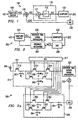
- FIG. 1 a block diagram illustrates a first order sigma-delta ADC 100.
- Figure 1 a displays a sigma-delta ADC 100 with a sampling circuit 105.
- the sampling circuit 105 is typically not considered to be a part of a sigma-delta ADC 100.
- the sampling circuit 105 provides a discrete-time sample stream, x[n], from a continuous time (analog) signal, x(t).
- a commonly used sampling technique is a sample and hold circuit, which holds the value of its input signal for a specified amount of time. After the amount of time expires, the track-and-hold circuit holds the current value of its input signal for an additional amount of time.
- Figure 1 labels the names of the signals on the interconnections between functional blocks of the sigma-delta ADC 100.
- signal x[n] represents a discrete-time sample stream of the analog signal x(t).
- the discrete-time sample stream, x[n] is integrated (summed) by a discrete-time integrator 110.
- the discrete-time integrator 110 integrates (sums) an error sample stream, u[n]. This is because in the initial iteration, the difference sample stream, y a [n], is equal to zero.
- the discrete-time integrator 110 is implemented as a delay block (represented as a delay in the z-domain, z -1 ) 115 and a summing point 117.
- the output of the discrete-time integrator 110 becomes an input to a quantizer 120.
- the quantizer 120 is normally a single-bit quantizer, but it is possible to use a multi-bit quantizer.
- the quantizer 120 takes the output of the discrete-time integrator 110 and converts it into a digital bit value.
- the output of the quantizer 120, y[n] is also the output of the sigma-delta ADC 100.
- the output of the quantizer 120 is also fed back into the summing node 140, through a digital-to-analog converter (DAC) 130.
- the DAC 130 converts the digital value, y[n], back into an analog value, y a [n], that is subtracted from the discrete-time sample stream, x[n]. The subtraction is performed at a summing point 140.
- the operation of a first order sigma-delta ADC is considered well understood by those of ordinary skill in the art of the present invention and will not be discussed further.
- FIG. 2 a block diagram illustrates a general block diagram of a sigma-delta mixer 200 with a switched capacitor sampling circuit and the sigma-delta mixer 200 being constructed using switched capacitors according to a preferred embodiment of the present invention.
- a sampling circuit 210 is used to convert a continuous-time analog signal, x(t), into a discrete-time sample stream, x[n].
- the discrete-time sample stream, x[n] is then provided to a discrete-time signal processing unit 220, whose function may include gain control and/or filtering.
- the order of the sigma-delta mixer 200 can vary. If the discrete-time signal processing unit 220 performs first order integration, then the sigma-delta mixer 200 behaves similarly to a first order sigma-delta ADC. After being filtered (and possibly gain controlled), the discrete-time sample stream is forwarded to a quantizer 230.
- the quantizer 230 may be a single-bit or a multi-bit quantizer.
- a single-bit quantizer simply converts a sample value into one of two values, typically either a +1 or a -1, depending on the value of the sample.
- the output of the quantizer 230 is a digital data stream, y[n], and is also the output of the sigma-delta mixer 200.
- the output of the quantizer 230 is fedback into the sampling circuit 210 for use in generating subsequent outputs of the sigma-delta mixer 200.
- the digital data stream, y[n] is fedback into the sigma-delta mixer 200 through a feedback loop.
- a digital-to-analog converter (DAC) 240 In the feedback loop is a digital-to-analog converter (DAC) 240.
- the DAC 240 converts the digital data stream, y[n], into a discrete-time sample stream, y a [n].
- the discrete-time sample stream is then provided to a feedback mechanism 250 that is used to combine of the discrete-time sample stream, y a [n], with the discrete-time sample stream of the input signal, x[n]. Since sampling circuit 210 uses switched capacitors, the combination of the two discrete-time sample streams, y a [n] and x[n], is not accomplished by simply adding (or subtracting) the two discrete-time sample streams.
- FIG. 3a a block diagram illustrates a portion of a first order sigma-delta mixer 300 with switched capacitor sampling and feedback circuits where the mixer/sampling circuit is outside of the feedback loop according to a preferred embodiment of the present invention.
- Figure 3a displays a single signal path through a sigma-delta mixer that uses a switched capacitor sampling circuit and a switched capacitor feedback circuit with the sampling circuit not a part of the feedback loop.
- differential signaling the actual signal is carried on two different signals (and signal lines), one is referred to as a positive signal and the other is a negative signal.
- a second signal path is added.
- the second signal path is essentially identical to the signal path as displayed and persons of ordinary skill in the art of the present invention can readily see how to extend the sigma-delta mixer of Figure 3a into a sigma-delta mixer that uses differential signaling.
- the sigma-delta mixer 300 includes a transconductance amplifier (TA) 305 that provides a radio frequency (RF) current.
- the RF current represents the signal that is to be converted into digital form.
- the RF current may be brought to the TA 305 by an antenna (not shown) or some other RF source (also not shown).
- the RF current is then forwarded to a sampling circuit 310.
- the sampling circuit 310 is implemented using switched capacitors. The use of switched capacitors in a sampling circuit is explored in greater detailed in a copending non-provisional patent application entitled "Sampling Mixer with Asynchronous Clock and Signal Domains", filed 04/12/2002.
- the RF current is integrated by a history capacitor 307, C H , i.e., a charge is accumulated on the history capacitor 307.
- the flow of the RF current to the history capacitor 307 is controlled by a switch 312.
- the switch 312 is preferably coupled to a signal generated by a local oscillator (LO) and closes whenever the signal generated by the LO is positive.
- the signal is referred to as LO+.
- the switch 312 is controlled by a signal generated by a digital control unit (DCU) 317.
- DCU digital control unit
- each of the rotating capacitors 308 and 309 displayed in Figure 3a is actually a bank of M (preferably, four) rotating capacitors.
- Figure 3a displays the capacitance value of the two rotating capacitors 308 and 309 as M*C R , where C R is the capacitance of a single rotating capacitor. At any given time, however, only one of the rotating capacitors plus the history capacitor 307 is integrating the RF current.
- the ratio of the capacitance of C H to C R is greater than or equal to 50.
- the control and selection of the particular rotating capacitor used to integrate the RF current is performed by the DCU 317.
- the DCU 317 controls and selects the rotating capacitors through the use of switches 314 and 315.
- switches 314 and 315 According to a preferred embodiment of the present invention, when the DCU 317 selects a particular rotating capacitor, it deactivates all of the other rotating capacitors and activates only the chosen rotating capacitors.
- the history capacitor 307 integrates the RF current once every RF cycle rather than continuously integrating the RF current.
- the DCU 317 also controls the history capacitor 307 through the use of the RF switch 312.
- the charge accumulated on the rotating capacitors is read out.
- the read out charge provides a single discrete-time sample of the RF current.
- the rotating capacitors are reset and a bias voltage is preset on the rotating capacitors. The use of the rotating capacitors and the charge reset and voltage preset is explored in great detail in another non-provisional patent application entitled "Efficient Charge Transfer Using a Switched Capacitor Resistor", filed 05/16/2002.
- the sampling circuit 310 By periodically reading out the charge accumulated by the rotating capacitors, the sampling circuit 310 produces a discrete-time sample stream, u[n] (the difference of the discretized input signal, x[n], and the feedback signal, y a [n] (this is displayed functionally in Figure 1 )). After each discrete-time sample is produced, it is then provided to a discrete-time analog signal processing unit (DTASP) 320.
- the DTASP 320 can be used to perform gain control and filtering among other operations.
- the DTASP 320 is implemented using switched capacitors and buffers. Due to its implementation from switched capacitors and buffers, the DTASP 320 operates via charge sharing in a fashion similar to the sampling circuit 310.
- FIG. 4 a diagram illustrates the use of an active buffer 405 to realize an infinite-impulse response (IIR) filtering stage 400 in a DTASP 320 according to a preferred embodiment of the present invention.
- the buffer 405 actually does not play an active role in the IIR filtering operation. Rather, it is used to sense voltage from a buffer capacitor 410, C B , and to present it to the output with a low driving impedance.
- An RF switch 415 couples the rotating capacitors 420 (displayed here as a single capacitor of value M*C R ) to the buffer capacitor 410 during the charge read out phase.
- the switch 415 opens, disconnecting the rotating capacitors 420 from the capacitor 410. After being disconnected, the rotating capacitors 420 have their charge reset. It is the resetting of the charge stored on the rotating capacitors that gives rise to the IIR filtering operation.
- the IIR filtering operation is of a first order. Should gain control be desired, a gain can be achieved either through active or passive means at the output buffer 405.
- the output of the DTASP 320 is then provided to a quantizer 330.
- the quantizer 330 is used to convert an analog value (in this case, an analog sample value) into a digital value. For example, if the quantizer 330 is a single bit quantizer, then it compares the analog value against a threshold. If the analog value is below the threshold, then the quantizer 330 would output one specified bit value and if the analog value is greater than or equal to the threshold, the quantizer would output the other bit value.
- Multi-bit quantizers operate in a similar manner, but they compare the analog value against 2 N - 1 thresholds, where N is the number of bits in the multi-bit quantizer, and produce one of 2 N possible bit values as output.
- a more traditional sigma-delta ADC integrator may be used.
- the DTASP 320 uses switched capacitors and an output buffer to provide filtering and possibly gain control.
- the more traditional sigma-delta ADC integrator would attach immediately after the history capacitors 308 and 309 and the switches 314 and 315 and before the quantizer 330.
- the quantizer 330 may also be similar to one that is usable in a conventional sigma-delta ADC. According to a preferred embodiment of the present invention, there are no special requirements or restrictions placed on the quantizer 330, i.e., an ordinary quantizer could be used.
- the output of the quantizer 330, y[n] is the output of the sigma-delta mixer 300. As described previously, the output of the quantizer 330 is also fedback into the sampling circuit 310 for use in the generation of a difference function between it and the input signal.
- the output of the quantizer 330, y[n], is a digital value and must be converted back into an analog value. This is accomplished via a digital-to-analog converter (DAC) 340.
- a current-mode DAC would be an example of a DAC usable as the DAC 340.
- a current-mode DAC produces a certain amount of current, dependant upon the digital value it is receiving as input.
- the current-mode DAC operates as a switchable current source.
- the DAC 340 can be configured to produce currents of different magnitude, rather than simply switching the current on and off. For example, if a k-bit quantizer were used rather than a single-bit quantizer, then the DAC 340 would produce one of 2 k different output values.
- the current produced by the DAC 340 is used by a feedback mechanism 350 to subtract the output of the quantizer 330, y[n], from the discrete-time sample stream, x[n]. Since the sampling circuit uses switched capacitors, y[n] cannot be simply subtracted from x[n].
- the current produced by the DAC 340 is integrated by a pre-feedback capacitor 351, C X . The integration of the current results in the accumulation of a charge on the pre-feedback capacitor 351. After the pre-feedback capacitor 351 integrates the current for a specified period of time, a pair of switches (353 or 355) is closed by control signals provided by the DCU 317.
- the charge accumulated on the buffer capacitor 351 is shared with one of two feedback capacitors (C F ) 352 or 354, depending upon the pair of switches closed.
- the charge shared with one of the feedback capacitors, C F is subsequently shared with one of the two rotating capacitors 308 or 309 (again, dependant upon which pair of switches are closed). It is through the charge shared with the rotating capacitors that the output of the quantizer, y[n], is subtracted from the discrete-time sample stream, x[n].
- the sampling structure of Figure 3a samples the RF current only when the signal LO+ is active. Therefore, if left alone, approximately half of the RF current is lost.
- a similar sampling structure (not shown), referred to as an inverse structure, with a switch that is controlled by an inverse of the LO+ signal (LO-), is used to sample the RF current when the structure as displayed in Figure 3a is inactive.
- the output of the two sampling structures provides a discrete-time sample stream of the complete RF current.
- the output of the inverse sampling structure is also provided to the DTASP 320. The DTASP 320 then combines the two discrete-time sample streams into one and uses it in further processing.
- FIG. 3b a diagram illustrates a sampling circuit 310 in greater detail according to a preferred embodiment of the present invention.
- the sampling circuit 310 as displayed in Figure 3a had a single merged sampling capacitor with a capacitance of M*C R , where C R is defined as the capacitance of a single rotating capacitor and M is the number of rotating capacitors in a single rotating capacitor bank.
- C R is defined as the capacitance of a single rotating capacitor
- M is the number of rotating capacitors in a single rotating capacitor bank.
- the purpose of displaying the sampling capacitor as a single merged capacitor is to simplify the diagram. It is actually preferred that the single sampling capacitor be replaces with a plurality of rotating capacitors.
- Figure 3b displays a preferred embodiment of the sampling circuit.
- Figure 3b displays only a portion of the sigma-delta mixer 300 displayed in Figure 3a.
- the portion of the sigma-delta mixer 300 includes the transconductance amplifier 305 and the sampling circuit 310.
- the sampling circuit 310 includes the switch 312 that is driven by the signal generated by the local oscillator and the history capacitor 307.
- the sampling capacitors 308 and 309 are each replaced with a rotating capacitor bank.
- Each rotating capacitor bank has several rotating capacitors, in this case, there are four rotating capacitors in each rotating capacitor bank.
- the sampling capacitor 308 now is a bank of four rotating capacitors, for example, rotating capacitor 316.
- the switches 314 that are driven by the DCU 317 are replaced by a single switch 318.
- the switch 318 is also driven by the DCU 317 and is used to activate or deactivate the rotating capacitor 316.
- Another switch 319 is used to read out the charge accumulated on the rotating capacitor. While the sampling circuit displayed in Figure 3b is a preferred embodiment, use of the sampling circuit displayed in Figure 3a will result in a fully functional sigma-delta mixer.
- the presence of the buffer capacitor 351 is not necessary for proper operation of the present invention. If the buffer capacitor 351 is not present, then the current provided by the DAC 340 can be directly integrated by either of the feedback capacitors 352 or 354. As displayed in Figure 3a, the feedback provided could be a two-level feedback (+/- 1). This is the realization of a signal bit quantizer. The two-level feedback can be modified to provide multi-level feedback through the addition of additional DAC 340 outputs.
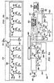
- FIG. 3c a block diagram illustrates a sigma-delta mixer 360 with switched capacitor sampling and feedback circuits where the sampling circuit is structurally outside of the feedback loop according to a preferred embodiment of the present invention. While Figure 3a displays a portion of a sigma-delta mixer, Figure 3c displays a complete sigma-delta mixer when quadrature-phased, differential mode is being used.
- the sigma-delta mixer 360 is essentially the same as the sigma-delta mixer 300 with the signal path replicated three additional times.
- the sigma-delta mixers presented in Figures 3a and 3b are configured so that the sampling circuit is structurally outside of the feedback loop. Alternatively, the sampling circuit can be brought structurally inside the feedback loop.
- FIG. 5 a diagram illustrates a high-level view of a sigma-delta mixer 500 with a switched capacitor sampling and feedback circuits where the sampling circuit is structurally inside the feedback loop according to a preferred embodiment of the present invention.
- the sigma-delta mixer 500 is similar in design to the sigma-delta mixer displayed in Figure 2 with the exception of the placement of the feedback loop. Rather than having the feedback be injected structurally after the sampling circuit, such as sampling circuit 210 ( Figure 2), the feedback is injected structurally prior to a sampling circuit, such as sampling circuit 510. Other functional blocks are essentially the same.
- FIG. 6a a block diagram illustrates a portion of a first order sigma-delta mixer 600 with a switched capacitor sampling and feedback circuits where a sampling circuit 610 is structurally inside the feedback loop according to a preferred embodiment of the present invention.
- the sigma-delta mixer 600 displays one signal path out of several required for a sigma-delta mixer 600 that operates with differential signaling.
- the sigma-delta mixer 600 includes a transconductance amplifier (TA) 605 that provides a RF current.
- the RF current is forwarded to the sampling circuit 610 that is responsible for sampling the RF current and providing a discrete-time sample stream representation of the RF current.
- the flow of the RF current is controlled by a switch 611.
- the switch 611 is driven by a signal generated by a local oscillator (LO).
- LO local oscillator
- DCU digital control unit
- the sampling circuit 610 is created using switched capacitors and a detailed explanation of the operation is provided above.
- the discrete-time sample stream is provided to a discrete-time analog signal processing unit (DTASP) 615.
- the DTASP 615 is used to provide gain control and filtering.
- the DTASP 615 is configured to provide a first order filtering operation, hence providing the filtering required for a first order sigma-delta ADC.
- the output of the DTASP 615 is then converted into a digital data stream by a quantizer 617.
- the quantizer 617 is a single-bit quantizer.
- the output of the quantizer 617 is provided to a digital signal processing unit (DSP) 619.
- the DSP 619 is used to provide additional filtering of the output of the quantizer.
- the output of the DSP 619 is the output of the sigma-delta mixer 600.
- the output of the quantizer 617 is also used to provide feedback to a point structurally prior to the sampling circuit 610.
- the output of the quantizer 617 is subtracted from the input signal to provide a difference function that is subsequently converted into a digital bit stream.
- the output of the quantizer 617 is converted back into an analog signal by a digital-to-analog converter (DAC) 622.
- the analog signal is then provided to a feedback mechanism 620.
- the sampling circuit 610 uses switched capacitors and therefore, the analog signals provided by the DAC 622 may not be simply subtracted from the input signal. Rather, the DAC 622 produces a current corresponding to the output of the quantizer 617 and the current is integrated by a pre-feedback capacitor 623, C X . After the pre-feedback capacitor 623 integrates the current for a specified period of time, a pair of switches (626 or 627) is closed by control signals provided by the DCU 609.
- the charge accumulated on the pre-feedback capacitor 623 is shared with one of two feedback capacitors (C F ) 624 or 625, depending upon the pair of switches closed.
- the charge shared with one of the feedback capacitors, C F is subsequently shared with the history capacitor 606, C H . It is through the charge shared with the history capacitor that the output of the quantizer, y[n], is subtracted from the discrete-time sample stream, x[n].
- the presence of the pre-feedback capacitor 623 is not necessary for proper operation of the present invention. If the pre-feedback capacitor 623 is not present, then the current provided by the DAC 622 can be directly integrated by either of the feedback capacitors 624 or 625. As displayed in Figure 6a, the feedback provided may be a two-level feedback (+/- 1). This is the realization of a signal bit quantizer. The two-level feedback can be modified to provide multi-level feedback through the addition of additional DAC 622 outputs.
- FIG. 6b a block diagram illustrates a sigma-delta mixer 650 with a switched capacitor sampling and feedback circuits where the sampling circuit is structurally inside the feedback loop according to a preferred embodiment of the present invention. While Figure 6a displays a portion of a sigma-delta ADC, Figure 6b displays a complete sigma-delta mixer when quadrature-phased, differential signaling is being used.
- the sigma-delta mixer 650 is essentially the same as the sigma-delta mixer 600 with the signal path replicated three additional times.
- Figures 3a-b and 6a-b display sigma-delta mixers that use charge sharing to complete the feedback loop.
- Charge sharing is an efficient way to feed the output of the quantizer, y[n], back to the sampling circuit so that y[n] can be subtracted from the input to provide the difference function that is then integrated.
- charge sharing is not the only way to accomplish the feedback mechanism.
- the feedback loop can also be completed using charge injection.
- the sigma-delta mixer 700 includes a transconductance amplifier (TA) 705 coupled to a history capacitor 710 and sampling capacitors 716.
- TA transconductance amplifier
- the sampling capacitors 716 have been referred to as rotating capacitors and typically, there are multiple rotating capacitors arrange in capacitor banks.
- the sampling capacitors 716 may be multiple banks of rotating capacitors.
- DCU digital control unit
- the history capacitor 710 and the sampling capacitors 716 form a sampling circuit and are used to convert a RF current provided by the TA 705 into a discrete-time sample stream.
- the flow of the RF current is regulated by a switch 712, which is controlled by a signal generated by a local oscillator (LO), LO+.
- LO local oscillator
- the discrete-time sample stream is then provided to a discrete-time analog signal processing unit (DTASP) 720 wherein the discrete-time sample stream may be gain controlled and filtered.
- DTASP discrete-time analog signal processing unit
- the output of the DTASP 720 is provided to a quantizer 725, which converts the discrete-time sample stream into a digital bit stream.
- the output of the quantizer 725 is the output of the sigma-delta mixer 700. Additionally, the output of the quantizer 725 is used to provide feedback information to the sampling circuit
- the feedback mechanism as previously described uses charge sharing to combine (subtract) the output of the quantizer 725 from the input signal.
- the sigma-delta mixer 700 uses charge injection to accomplish a similar result.
- the output of the quantizer 725 is provided to a current steering DAC 730.
- the DAC 730 converts the output of the quantizer 725 into a current of specified magnitude.
- the current produced by the DAC 730 is equal to gm*v FB where gm is a transconductance gain and v FB is a voltage provided by the output of the quantizer 725.
- the current produced by the DAC 730 is directed to the history capacitor 710 by a switch 742.
- the switch 742 is controlled by an inverse of the signal generated by the LO, LO-, in a fashion similar to the switch 712. When the signal LO- is high, the switch 742 closes and the current produced by the DAC 730 is integrated by the history capacitor 710 and the sampling capacitors 716.
- the current produced by the DAC 730 is also directed to a dummy capacitor 740 by another switch 744.
- the switch 744 is driven preferably by the signal generated by the LO, LO+.
- the signals LO+ and LO- are inverses of one another, i.e., when the signal LO+ is active, the signal LO- is inactive and vice versa.
- the current produced by the DAC 730 is either directed to the history capacitor 710 or to the dummy capacitor 740.
- the sigma-delta mixer 700 is discarding the output of the quantizer 725 (by integrating the current produced by the DAC 730 with the dummy capacitor 740) when LO+ is active.
- the output of the quantizer 725 are discarded when LO+ signal is active, the information carried in the current when the LO+ signal is active is not lost since there is preferably a similar structure to that shown in Figure 7 that discards the output of the quantizer 725 when LO- is active.
- the two structures provide (in the form of feedback) all of the output produced by the quantizer 725.
- a first order sigma-delta ADC provides a first order filtering of the signal that it is converting and a second order sigma-delta ADC provides a second order filtering of the signal that it is converting.
- a second order sigma-delta ADC (and higher order ones for that matter) cannot be created by simply cascading first order sigma-delta ADCs.
- a block diagram illustrates a second order sigma-delta ADC 800.
- the order of a sigma-delta ADC refers to the order of the filtering performed by the sigma-delta ADC.
- the first order sigma-delta ADC 100 illustrated in Figure 1 has effectively a first order filter that is created in the discrete-time integrator. Therefore, a second order sigma-delta ADC, such as one displayed in Figure 8 has a behavior that corresponds to a second order filter.
- the second order sigma-delta ADC 800 has a first discrete-time integrator 815 that provides a first order filter.
- the second order sigma-delta ADC 800 has a second discrete-time integrator 810. It is the second discrete-time integrator 810, in conjunction with the first discrete-time integrator 815 that provides a second first order filter. When cascaded, the two first order filters become a second order filter. By cascading additional filter sections, sigma-delta ADCs of order greater than two can be created.
- FIG. 9 a diagram illustrates a second-order sigma-delta mixer 900 with a switched capacitor sampling circuit 902 according to a preferred embodiment of the present invention.
- the switched-capacitor sampling circuit 902 is similar to the switched capacitor sampling circuit for the first-order sigma-delta mixer discussed previously.
- the switched-capacitor sampling circuit 902 includes a sampling capacitor 910 that is controlled by a pair of switches 915 and 922.
- the first switch 915 regulates the flow of the signal current to the sampling capacitor 910 and is controlled by a signal generated by a local oscillator (LO) and is referred to as LO+.
- LO local oscillator
- the switch 915 is active whenever LO+ is active.
- the switch 915 Whenever the switch 915 is active, the signal provided by a transconductance amplifier 905 flows and is integrated by the sampling capacitor 910.
- the second switch 922 is controlled by a digital control unit (DCU) 920.
- the DCU 920 controls the operation of the sampling capacitor 910.
- the DCU 920 controls when the charge accumulated on the sampling capacitor 910 is read out, providing a discrete-time sample.
- the switched-capacitor sampling circuit 902 can be replaced with one of the previously discussed switched-capacitor sampling circuits wherein the single sampling capacitor 910 is replaced with a history capacitor and several banks of rotating capacitors.
- the switched-capacitor sampling circuit 902 When the switched-capacitor sampling circuit 902 is configured as a combination of a history capacitor and several banks of rotating capacitors, the switched-capacitor sampling circuit 902 performs a filtering operation on the signal provided by the transconductance amplifier 905. This filtering operation is a first-order operation and provides one of the two first-order filtering operations required in a second-order sigma-delta mixer.
- the discrete-time sample stream produced by the switched-capacitor sampling circuit 902 is provided to a first discrete-time analog signal processing circuit (DTASP) 925.
- the DTASP 925 is similar to the DTASP discussed previously in conjunction with first-order sigma-delta mixers. As previously discussed, the DTASP 925 can be configured to provide gain control and filtering. The operation of the DTASP 925 is controlled by signals provided by the DCU 920.
- a second-order sigma-delta ADC has two integrators.
- the DTASP 925 provided one of the two integrators.
- a second integrator another DTASP
- a second sampling capacitor 929 is inserted between the first DTASP 925 and a second DTASP 930.
- the second sampling capacitor 929 is used to integrate the current provided by the first DTASP 925, which is a discrete-time sample stream. It is the charge accumulated on the second sampling capacitor that is read out and provided to the second DTASP 930.
- the second sampling capacitor 929 also accumulates feedback information. The feedback information and how it is provided to the second sampling capacitor will be discussed below.
- the second DTASP 930 can be configured to provide gain control and/or filtering.
- the second DTASP 930 is configured to operate as a first-order filter. Therefore, when combined with the first-order filtering provided by the switched-capacitor sampling circuit 902, the necessary filtering of order two is provided.
- the output of the second DTASP 930 is provided to a quantizer 935.
- the output of the quantizer 935 is the output of the second-order sigma-delta mixer 900.
- the operation of the second DTASP 930 is also controlled by the DCU 920.
- the output of the quantizer 935 is also used to provide feedback information. As is displayed in Figure 8, there are two feedback loops in a second-order sigma-delta mixer, one for each integrator. Because the two integrators (previously referred to as DTASPs) use switched capacitors, the feedback information cannot be simply combined with the inputs of the integrators. The feedback information must be combined with the inputs of the integrators through a charge sharing (or charge injection) mechanism as discussed previously.
- a digital-to-analog converter (DAC) 940 is used to convert the output of the quantizer 935 into a current that is integrated by the sampling capacitors at the inputs of the integrators. The output of the DAC 940 is controlled by switches 942 and 944.
- the first switch 942 controls the output of the DAC 940 that coupled to the first sampling capacitor 910.
- the switch 942 itself, is controlled by the inverse of the signal controlling the switch 915.
- the LO- signal permits the current provided by the DAC 940 to be integrated by the sampling capacitor 910 when the switch 915 prevents the signal provided by the transconductance amplifier 905 from flowing.
- a second switch 944 controlled by the DCU 920, controls the flow of the current produced by the DAC 940 to the second sampling capacitor 929.
Landscapes
- Engineering & Computer Science (AREA)
- Theoretical Computer Science (AREA)
- Compression, Expansion, Code Conversion, And Decoders (AREA)
Abstract
Description
Claims (10)
- A circuit to provide a discrete-time sample stream, the circuit comprising:a switch to regulate the flow of a signal, the switch controlled by a control signal;a history capacitor coupled to the switch, the history capacitor to integrate the signal when the switch permits the flow of the signal;at least two rotating capacitors coupled in a parallel fashion to the history capacitor, the rotating capacitors to integrate the signal and the signal accumulated on the rotating capacitors is read out to produce a sample; anda feedback signal line coupled to the rotating capacitors.
- The circuit of claim 1, wherein the history capacitor and one of the rotating capacitors is integrating the signal at any given time.
- The circuit of claims 1 or 2, wherein each rotating capacitor is a bank of M rotating capacitors, where M is an integer number.
- The circuit of claims 1, 2 or 3, wherein each rotating capacitor has a capacitance value of CR and the history capacitor has a capacitance value of CH, and the capacitance value of CR is much smaller than the capacitance value of CH.
- The circuit of claim 4, wherein each rotating capacitor is controlled by a separate switch coupled to a control signal.
- A sigma-delta mixer comprising:a signal input;a sampling circuit that operates in a discrete-time charge domain, coupled to the signal input, the sampling circuit containing circuitry to convert a signal provided by the signal input into a discrete-time sample stream (DTSS);a discrete-time processing unit coupled to the sampling unit, the discrete time processing unit containing circuitry to filter the discrete-time sample stream; anda feedback signal line coupled to the discrete-time processing unit and the sampling unit, the feedback signal line to carry information outputted by the discrete-time processing unit to the sampling unit.
- The sigma-delta mixer of claim 6, wherein the discrete-time processing unit comprises:a discrete-time signal processing unit coupled to the sampling circuit, the discrete-time signal processing unit containing circuitry to filter the discrete-time sample stream; anda quantizer coupled to the discrete-time signal processing unit, the quantizer containing circuitry to digitize the filtered discrete-time sample stream.
- The sigma-delta mixer of claim 6 or 7, wherein the discrete-time processing unit also contains circuitry to gain control the discrete-time sample stream.
- The sigma-delta mixer of claim 6, 7, or 8 further comprising a digital-to-analog converter coupled having an input coupled to the discrete-time processing unit and an output coupled to the feedback signal line, the digital-to-analog converter to convert a digital signal into an analog signal.
- The sigma-delta mixer of claim 6, 7, 8 or 9, wherein:the discrete-time processing unit (DTP) comprises:a discrete-time analog signal processing unit (DTASP) coupled to the sampling unit, the DTASP containing circuitry to filter the DTSS;a quantizer coupled to the DTASP, the quantizer to convert an output produced by the DTASP into a digital value;the sigma-delta mixer further comprising:a digital-to-analog converter (DAC) coupled to the output of the quantizer, the DAC to convert an output of the quantizer into an analog signal; anda feedback mechanism coupled to the DAC, having an output coupled to the feedback signal line, the feedback mechanism containing circuitry to convert the analog signal produced by the DAC into a feedback signal that is combined with the input signal.
Priority Applications (1)
| Application Number | Priority Date | Filing Date | Title |
|---|---|---|---|
| EP06117965A EP1724929A1 (en) | 2002-10-17 | 2003-10-17 | A Sigma-Delta (SD) Analog-To-Digital Converter (ADC) structure incorporating a direct sampling mixer |
Applications Claiming Priority (2)
| Application Number | Priority Date | Filing Date | Title |
|---|---|---|---|
| US10/273,217 US7057540B2 (en) | 2001-10-26 | 2002-10-17 | Sigma-delta (ΣΔ) analog-to-digital converter (ADC) structure incorporating a direct sampling mixer |
| US273217 | 2008-11-18 |
Related Child Applications (1)
| Application Number | Title | Priority Date | Filing Date |
|---|---|---|---|
| EP06117965A Division EP1724929A1 (en) | 2002-10-17 | 2003-10-17 | A Sigma-Delta (SD) Analog-To-Digital Converter (ADC) structure incorporating a direct sampling mixer |
Publications (3)
| Publication Number | Publication Date |
|---|---|
| EP1411639A2 true EP1411639A2 (en) | 2004-04-21 |
| EP1411639A3 EP1411639A3 (en) | 2005-01-19 |
| EP1411639B1 EP1411639B1 (en) | 2008-03-26 |
Family
ID=32042950
Family Applications (2)
| Application Number | Title | Priority Date | Filing Date |
|---|---|---|---|
| EP03103860A Expired - Lifetime EP1411639B1 (en) | 2002-10-17 | 2003-10-17 | A Sigma-Delta (SD) Analog-To-Digital Converter (ADC) structure incorporating a direct sampling mixer |
| EP06117965A Withdrawn EP1724929A1 (en) | 2002-10-17 | 2003-10-17 | A Sigma-Delta (SD) Analog-To-Digital Converter (ADC) structure incorporating a direct sampling mixer |
Family Applications After (1)
| Application Number | Title | Priority Date | Filing Date |
|---|---|---|---|
| EP06117965A Withdrawn EP1724929A1 (en) | 2002-10-17 | 2003-10-17 | A Sigma-Delta (SD) Analog-To-Digital Converter (ADC) structure incorporating a direct sampling mixer |
Country Status (4)
| Country | Link |
|---|---|
| US (1) | US7057540B2 (en) |
| EP (2) | EP1411639B1 (en) |
| JP (1) | JP2004289793A (en) |
| DE (1) | DE60319935T2 (en) |
Cited By (4)
| Publication number | Priority date | Publication date | Assignee | Title |
|---|---|---|---|---|
| WO2007049199A1 (en) * | 2005-10-26 | 2007-05-03 | Nxp B.V. | Electronic device for receiving rf signals and method for rf sampling |
| US7962115B2 (en) | 2007-12-31 | 2011-06-14 | Industrial Technology Research Institute | Circuit with programmable signal bandwidth and method thereof |
| US8340617B2 (en) | 2007-12-12 | 2012-12-25 | Panasonic Corporation | Sampling mixer, quadrature demodulator, and wireless device |
| US8385874B2 (en) | 2007-03-06 | 2013-02-26 | Panasonic Corporation | Discrete time direct sampling circuit and receiver |
Families Citing this family (51)
| Publication number | Priority date | Publication date | Assignee | Title |
|---|---|---|---|---|
| US7006813B2 (en) * | 2001-08-15 | 2006-02-28 | Texas Instruments Incorporated | Efficient charge transfer using a switched capacitor resistor |
| US7519135B2 (en) * | 2001-08-15 | 2009-04-14 | Texas Instruments Incorporated | Direct radio frequency (RF) sampling with recursive filtering method |
| US8027657B2 (en) * | 2001-10-26 | 2011-09-27 | Texas Instruments Incorporated | Sampling mixer with asynchronous clock and signal domains |
| US20040223553A1 (en) * | 2003-02-07 | 2004-11-11 | Kumar Derek D. | Method and system for wireless audio transmission using low bit-weight words |
| US7304591B2 (en) * | 2003-08-13 | 2007-12-04 | Sandlinks Systems Ltd. | Method and system for providing a digital signal representing an analog signal |
| US7006023B2 (en) * | 2003-09-12 | 2006-02-28 | Texas Instruments Inc. | Sigma-delta modulator with passive bandpass loop filter |
| US7382834B2 (en) * | 2004-05-06 | 2008-06-03 | Beceem Communications Inc. | Phase rotation estimation |
| DE602004009779T2 (en) * | 2004-07-09 | 2008-08-28 | Stmicroelectronics S.R.L., Agrate Brianza | Device for converting an analog signal into a digital signal, corresponding method and voltage regulator control circuit with this device |
| JP2006140825A (en) | 2004-11-12 | 2006-06-01 | Sanyo Electric Co Ltd | Trap filter |
| JP5022672B2 (en) * | 2005-11-22 | 2012-09-12 | パナソニック株式会社 | Sampling mixer and receiver |
| US7605733B2 (en) * | 2005-12-13 | 2009-10-20 | Nxp B.V. | Radio frequency ΣΔ-modulator |
| US7436338B2 (en) * | 2005-12-21 | 2008-10-14 | Slicex, Inc. | Current mode sigma-delta modulator |
| DE102005061813B4 (en) * | 2005-12-23 | 2012-10-11 | Intel Mobile Communications GmbH | receiver circuit |
| JP5270110B2 (en) * | 2006-05-24 | 2013-08-21 | パナソニック株式会社 | Mixer with frequency selection function |
| US7671658B2 (en) * | 2006-05-24 | 2010-03-02 | Panasonic Corporation | Mixer having frequency selection function |
| WO2007142341A1 (en) | 2006-06-08 | 2007-12-13 | Panasonic Corporation | Discrete filter, sampling mixer, and radio device |
| WO2007148693A1 (en) * | 2006-06-20 | 2007-12-27 | Panasonic Corporation | Discrete filter, sampling mixer, and radio device |
| GB0617848D0 (en) * | 2006-09-11 | 2006-10-18 | Global Silicon Ltd | A random number generator |
| JP4692461B2 (en) * | 2006-10-11 | 2011-06-01 | ソニー株式会社 | Receiver, receiving method, filter circuit, control method |
| US7822389B2 (en) * | 2006-11-09 | 2010-10-26 | Texas Instruments Incorporated | Methods and apparatus to provide an auxiliary receive path to support transmitter functions |
| JP4296518B2 (en) * | 2006-12-07 | 2009-07-15 | ソニー株式会社 | Information processing apparatus and information processing method |
| US7973586B2 (en) * | 2007-03-29 | 2011-07-05 | Panasonic Corporation | Sampling mixer, filter device, and radio device |
| US7495595B2 (en) * | 2007-04-30 | 2009-02-24 | Infineon Technologies Ag | Analog-to-digital converter, receiver arrangement, filter arrangement and signal processing method |
| US7904048B2 (en) * | 2007-06-29 | 2011-03-08 | Texas Instruments Incorporated | Multi-tap direct sub-sampling mixing system for wireless receivers |
| JP4954150B2 (en) | 2007-07-05 | 2012-06-13 | パナソニック株式会社 | Discrete filter, sampling mixer, and radio apparatus |
| US8380781B2 (en) * | 2007-07-18 | 2013-02-19 | Panasonic Corporation | Sampling filter and radio communication apparatus |
| GB2452524A (en) * | 2007-09-06 | 2009-03-11 | Cambridge Silicon Radio Ltd | A jitter insensitive sigma-delta modulator |
| WO2009031886A2 (en) * | 2007-09-07 | 2009-03-12 | Fujifilm Manufacturing Europe B.V. | Method and apparatus for atomic layer deposition using an atmospheric pressure glow discharge plasma |
| WO2009041047A1 (en) * | 2007-09-27 | 2009-04-02 | Panasonic Corporation | Sampling filter device |
| US7489263B1 (en) * | 2007-09-28 | 2009-02-10 | Cirrus Logic, Inc. | Discrete-time programmable-gain analog-to-digital converter (ADC) input circuit with multi-phase reference application |
| US7492296B1 (en) | 2007-09-28 | 2009-02-17 | Cirrus Logic, Inc. | Discrete-time programmable-gain analog-to-digital converter (ADC) input circuit with input signal and common-mode current nulling |
| TWI358911B (en) * | 2007-12-24 | 2012-02-21 | Ind Tech Res Inst | Receiver with discrete-time down-conversion and fi |
| JP4978550B2 (en) * | 2008-04-28 | 2012-07-18 | トヨタ自動車株式会社 | Mixer and ΔΣ modulator |
| JP4978549B2 (en) * | 2008-04-28 | 2012-07-18 | トヨタ自動車株式会社 | Mixer and ΔΣ modulator |
| US8542616B2 (en) * | 2008-10-14 | 2013-09-24 | Texas Instruments Incorporated | Simultaneous multiple signal reception and transmission using frequency multiplexing and shared processing |
| US8433276B2 (en) * | 2008-12-03 | 2013-04-30 | Panasonic Corporation | Sampling circuit and receiver |
| JP5355589B2 (en) * | 2008-12-04 | 2013-11-27 | パナソニック株式会社 | Sampling circuit and receiver using the same |
| WO2010087199A1 (en) | 2009-01-29 | 2010-08-05 | パナソニック株式会社 | Harmonic rejection mixer |
| JP5622592B2 (en) | 2009-01-29 | 2014-11-12 | パナソニック株式会社 | Polyphase mixer |
| KR20100133748A (en) * | 2009-06-12 | 2010-12-22 | 삼성전자주식회사 | Discrete time filter and receiver containing it |
| JP5607904B2 (en) * | 2009-08-31 | 2014-10-15 | パナソニック株式会社 | Direct sampling circuit and receiver |
| EP2555433A4 (en) * | 2010-04-01 | 2014-06-04 | Japan Science & Tech Agency | METHOD OF CONVERTING DATA BASED ON -MAP SCALE |
| JP5623877B2 (en) * | 2010-11-15 | 2014-11-12 | ルネサスエレクトロニクス株式会社 | Semiconductor integrated circuit and operation method thereof |
| US8643528B1 (en) * | 2012-08-02 | 2014-02-04 | Texas Instruments Incorporated | Analog-to-digital converter |
| US10148253B2 (en) | 2015-05-11 | 2018-12-04 | The Trustees Of Columbia University In The City Of New York | Circuits for switched capacitor receiver front-ends |
| JP2016225840A (en) * | 2015-05-29 | 2016-12-28 | 株式会社東芝 | Amplifier circuit, ad converter, radio communication device, and sensor system |
| JP2017046058A (en) * | 2015-08-24 | 2017-03-02 | 株式会社東芝 | AD converter, analog front end, and sensor system |
| US10298245B1 (en) * | 2018-03-16 | 2019-05-21 | Synaptics Incorporated | Audio analog-to-digital converter systems and methods |
| US10305507B1 (en) * | 2018-03-20 | 2019-05-28 | Texas Instruments Incorporated | First-order sigma-delta analog-to-digital converter |
| US10972319B2 (en) * | 2018-09-12 | 2021-04-06 | Texas Instruments Incorporated | Clockless decision feedback equalization (DFE) for multi-level signals |
| EP4152622B1 (en) | 2021-09-17 | 2025-07-30 | Nxp B.V. | A baseband receiver circuit |
Family Cites Families (12)
| Publication number | Priority date | Publication date | Assignee | Title |
|---|---|---|---|---|
| US5039989A (en) | 1989-10-27 | 1991-08-13 | Crystal Semiconductor Corporation | Delta-sigma analog-to-digital converter with chopper stabilization at the sampling frequency |
| US5079550A (en) * | 1989-10-27 | 1992-01-07 | Crystal Semiconductor Corporation | Combining continuous time and discrete time signal processing in a delta-sigma modulator |
| US5068660A (en) * | 1989-10-27 | 1991-11-26 | Crystal Semiconductor Corporation | Combining fully-differential and single-ended signal processing in a delta-sigma modulator |
| US5640698A (en) * | 1995-06-06 | 1997-06-17 | Stanford University | Radio frequency signal reception using frequency shifting by discrete-time sub-sampling down-conversion |
| CA2157690A1 (en) | 1995-09-07 | 1997-03-08 | Bosco Leung | Lower power passive sigma-delta converter |
| US6037887A (en) * | 1996-03-06 | 2000-03-14 | Burr-Brown Corporation | Programmable gain for delta sigma analog-to-digital converter |
| US5691720A (en) * | 1996-03-08 | 1997-11-25 | Burr- Brown Corporation | Delta sigma analog-to-digital converter having programmable resolution/bias current circuitry and method |
| US6218972B1 (en) * | 1997-09-11 | 2001-04-17 | Rockwell Science Center, Inc. | Tunable bandpass sigma-delta digital receiver |
| US6040793A (en) | 1998-03-18 | 2000-03-21 | Analog Devices, Inc. | Switched-capacitor sigma-delta analog-to-digital converter with input voltage overload protection |
| JP4233761B2 (en) * | 1998-06-30 | 2009-03-04 | エヌエックスピー ビー ヴィ | Receiver with integrated mixer and sigma delta A / D converter |
| US6160859A (en) * | 1998-10-19 | 2000-12-12 | Motorola, Inc. | Integrated multi-mode bandpass sigma-delta receiver subsystem with interference mitigation and method of using the same |
| WO2002023732A2 (en) * | 2000-09-11 | 2002-03-21 | Broadcom Corporation | Methods and systems for high speed quantizers |
-
2002
- 2002-10-17 US US10/273,217 patent/US7057540B2/en not_active Expired - Lifetime
-
2003
- 2003-10-16 JP JP2003389948A patent/JP2004289793A/en active Pending
- 2003-10-17 DE DE60319935T patent/DE60319935T2/en not_active Expired - Lifetime
- 2003-10-17 EP EP03103860A patent/EP1411639B1/en not_active Expired - Lifetime
- 2003-10-17 EP EP06117965A patent/EP1724929A1/en not_active Withdrawn
Cited By (4)
| Publication number | Priority date | Publication date | Assignee | Title |
|---|---|---|---|---|
| WO2007049199A1 (en) * | 2005-10-26 | 2007-05-03 | Nxp B.V. | Electronic device for receiving rf signals and method for rf sampling |
| US8385874B2 (en) | 2007-03-06 | 2013-02-26 | Panasonic Corporation | Discrete time direct sampling circuit and receiver |
| US8340617B2 (en) | 2007-12-12 | 2012-12-25 | Panasonic Corporation | Sampling mixer, quadrature demodulator, and wireless device |
| US7962115B2 (en) | 2007-12-31 | 2011-06-14 | Industrial Technology Research Institute | Circuit with programmable signal bandwidth and method thereof |
Also Published As
| Publication number | Publication date |
|---|---|
| US7057540B2 (en) | 2006-06-06 |
| DE60319935D1 (en) | 2008-05-08 |
| US20030080888A1 (en) | 2003-05-01 |
| DE60319935T2 (en) | 2009-04-02 |
| EP1411639A3 (en) | 2005-01-19 |
| JP2004289793A (en) | 2004-10-14 |
| EP1724929A1 (en) | 2006-11-22 |
| EP1411639B1 (en) | 2008-03-26 |
Similar Documents
| Publication | Publication Date | Title |
|---|---|---|
| EP1411639B1 (en) | A Sigma-Delta (SD) Analog-To-Digital Converter (ADC) structure incorporating a direct sampling mixer | |
| US8063806B2 (en) | Apparatus comprising frequency selective circuit and method | |
| US7006813B2 (en) | Efficient charge transfer using a switched capacitor resistor | |
| KR100923481B1 (en) | Multibit Quantization Sigma Delta Modulator with Current-Mode Dynamic Element Matching and Dynamic Element Match Decision Logic | |
| JP4897825B2 (en) | Feedforward Sigma-Delta AD Converter with Optimal Built-in Filter Function | |
| US7129875B1 (en) | Tracking reference system for analog-to-digital converter systems | |
| US6346898B1 (en) | Multilevel analog to digital data converter having dynamic element matching in a reference data path | |
| US6121910A (en) | Frequency translating sigma-delta modulator | |
| US7528754B1 (en) | Finite impulse response digital to analog converter | |
| EP1980021B1 (en) | Continuous-time sigma-delta analog-to-digital converter with capacitor and/or resistance digital self-calibration means for rc spread compensation | |
| US7116260B2 (en) | Mismatch shaped analog to digital converter | |
| CA2502451C (en) | Mixed technology mems/bicmos lc bandpass sigma-delta for direct rf sampling | |
| US6518905B2 (en) | Parallel time interleaved delta sigma modulator | |
| US8248280B2 (en) | Successive approximation register (SAR) analog-to-digital converter (ADC) having optimized filter | |
| KR19990083479A (en) | Sigma-delta modulator and method for digitizing a signal | |
| US6864818B1 (en) | Programmable bandpass analog to digital converter based on error feedback architecture | |
| US7974363B2 (en) | Receiver, receiving method, filter circuit, and control method | |
| US8462030B2 (en) | Programmable loop filter for use with a sigma delta analog-to-digital converter and method of programming the same | |
| US7576670B2 (en) | Sigma-delta analog-digital converter for an xDSL multistandard input stage | |
| US6943715B2 (en) | Bandpass sigma-delta analog-to-digital converter and mash-sigma-delta converter incorporating same | |
| Yan et al. | A continuous-time/spl Sigma//spl Delta/modulator with 88dB dynamic range and 1.1 MHz signal bandwidth | |
| JP3367800B2 (en) | Selection device, A / D converter and D / A converter using the same | |
| US8994571B1 (en) | Compact high-speed analog-to-digital converter for both I and Q analog to digital conversion | |
| Jamin | RF receiver architecture state of the art | |
| Pelgrom | Time-Continuous Σ Δ Modulation |
Legal Events
| Date | Code | Title | Description |
|---|---|---|---|
| PUAI | Public reference made under article 153(3) epc to a published international application that has entered the european phase |
Free format text: ORIGINAL CODE: 0009012 |
|
| AK | Designated contracting states |
Kind code of ref document: A2 Designated state(s): AT BE BG CH CY CZ DE DK EE ES FI FR GB GR HU IE IT LI LU MC NL PT RO SE SI SK TR |
|
| AX | Request for extension of the european patent |
Extension state: AL LT LV MK |
|
| PUAL | Search report despatched |
Free format text: ORIGINAL CODE: 0009013 |
|
| AK | Designated contracting states |
Kind code of ref document: A3 Designated state(s): AT BE BG CH CY CZ DE DK EE ES FI FR GB GR HU IE IT LI LU MC NL PT RO SE SI SK TR |
|
| AX | Request for extension of the european patent |
Extension state: AL LT LV MK |
|
| 17P | Request for examination filed |
Effective date: 20050719 |
|
| AKX | Designation fees paid |
Designated state(s): DE FR GB |
|
| 17Q | First examination report despatched |
Effective date: 20050914 |
|
| GRAP | Despatch of communication of intention to grant a patent |
Free format text: ORIGINAL CODE: EPIDOSNIGR1 |
|
| GRAS | Grant fee paid |
Free format text: ORIGINAL CODE: EPIDOSNIGR3 |
|
| GRAA | (expected) grant |
Free format text: ORIGINAL CODE: 0009210 |
|
| AK | Designated contracting states |
Kind code of ref document: B1 Designated state(s): DE FR GB |
|
| REG | Reference to a national code |
Ref country code: GB Ref legal event code: FG4D |
|
| REF | Corresponds to: |
Ref document number: 60319935 Country of ref document: DE Date of ref document: 20080508 Kind code of ref document: P |
|
| ET | Fr: translation filed | ||
| PLBE | No opposition filed within time limit |
Free format text: ORIGINAL CODE: 0009261 |
|
| STAA | Information on the status of an ep patent application or granted ep patent |
Free format text: STATUS: NO OPPOSITION FILED WITHIN TIME LIMIT |
|
| 26N | No opposition filed |
Effective date: 20081230 |
|
| REG | Reference to a national code |
Ref country code: FR Ref legal event code: PLFP Year of fee payment: 14 |
|
| REG | Reference to a national code |
Ref country code: FR Ref legal event code: PLFP Year of fee payment: 15 |
|
| REG | Reference to a national code |
Ref country code: FR Ref legal event code: PLFP Year of fee payment: 16 |
|
| PGFP | Annual fee paid to national office [announced via postgrant information from national office to epo] |
Ref country code: FR Payment date: 20180920 Year of fee payment: 16 |
|
| PGFP | Annual fee paid to national office [announced via postgrant information from national office to epo] |
Ref country code: GB Payment date: 20180926 Year of fee payment: 16 |
|
| PGFP | Annual fee paid to national office [announced via postgrant information from national office to epo] |
Ref country code: DE Payment date: 20180917 Year of fee payment: 16 |
|
| REG | Reference to a national code |
Ref country code: DE Ref legal event code: R119 Ref document number: 60319935 Country of ref document: DE |
|
| PG25 | Lapsed in a contracting state [announced via postgrant information from national office to epo] |
Ref country code: DE Free format text: LAPSE BECAUSE OF NON-PAYMENT OF DUE FEES Effective date: 20200501 |
|
| GBPC | Gb: european patent ceased through non-payment of renewal fee |
Effective date: 20191017 |
|
| PG25 | Lapsed in a contracting state [announced via postgrant information from national office to epo] |
Ref country code: GB Free format text: LAPSE BECAUSE OF NON-PAYMENT OF DUE FEES Effective date: 20191017 Ref country code: FR Free format text: LAPSE BECAUSE OF NON-PAYMENT OF DUE FEES Effective date: 20191031 |