-
The present invention relates to a method of determining a stray radiation
condition, using a lithographic projection apparatus comprising a projection system with
a numerical aperture NA, the method comprising the steps of:
- supplying a projection beam of radiation, comprising radiation with a wavelength
λ,
- patterning the projection beam according to a pattern comprising a feature;
- projecting the patterned beam onto an image plane to create an image of said
feature.
-
The invention also relates to a lithographic projection apparatus operable
according to the above method.
-
The lithographic proj ection apparatus may comprise:
- a radiation system for supplying said projection beam of radiation;
- a support structure for supporting patterning means, the patterning means serving
to pattern the projection beam according to a desired pattern;
- a substrate table for holding a substrate; and
- a projection system for projecting the patterned beam with a magnification factor
M onto a target portion of the substrate.
-
The term "patterning means" as here employed should be broadly
interpreted as referring to means that can be used to endow an incoming radiation beam
with a patterned cross-section, corresponding to a pattern that is to be created in a target
portion of the substrate; the term "light valve" can also be used in this context. Generally,
the said pattern will correspond to a particular functional layer in a device being created
in the target portion, such as an integrated circuit or other device (see below). Examples
of such patterning means include:
- A mask. The concept of a mask is well known in lithography, and it includes
mask types such as binary, alternating phase-shift, and attenuated phase-shift, as well as
various hybrid mask types. Placement of such a mask in the radiation beam causes
selective transmission (in the case of a transmissive mask) or reflection (in the case of a
reflective mask) of the radiation impinging on the mask, according to the pattern on the
mask. In the case of a mask, the support structure will generally be a mask table, which
ensures that the mask can be held at a desired position in the incoming radiation beam,
and that it can be moved relative to the beam if so desired;
- A programmable mirror array. One example of such a device is a matrix-addressable
surface having a viscoelastic control layer and a reflective surface. The basic
principle behind such an apparatus is that (for example) addressed areas of the reflective
surface reflect incident light as diffracted light, whereas unaddressed areas reflect
incident light as undiffracted light. Using an appropriate filter, the said undiffracted light
can be filtered out of the reflected beam, leaving only the diffracted light behind; in this
manner, the beam becomes patterned according to the addressing pattern of the matrix-addressable
surface. An alternative embodiment of a programmable mirror array employs
a matrix arrangement of tiny mirrors, each of which can be individually tilted about an
axis by applying a suitable localized electric field, or by employing piezoelectric
actuation means. Once again, the mirrors are matrix-addressable, such that addressed
mirrors will reflect an incoming radiation beam in a different direction to unaddressed
mirrors; in this manner, the reflected beam is patterned according to the addressing
pattern of the matrix-addressable mirrors. The required matrix addressing can be
performed using suitable electronic means. In both of the situations described hereabove,
the patterning means can comprise one or more programmable mirror arrays. More
information on mirror arrays as here referred to can be gleaned, for example, from United
States Patents US 5,296,891 and US 5,523,193, and PCT patent applications
WO 98/38597 and WO 98/33096, which are incorporated herein by reference. In the case
of a programmable mirror array, the said support structure may be embodied as a frame
or table, for example, which may be fixed or movable as required; and
- A programmable LCD array. An example of such a construction is given in
United States Patent US 5,229,872, which is incorporated herein by reference. As above,
the support structure in this case may be embodied as a frame or table, for example,
which may be fixed or movable as required.
For purposes of simplicity, the rest of this text may, at certain locations, specifically
direct itself to examples involving a mask and mask table; however, the general
principles discussed in such instances should be seen in the broader context of the
patterning means as hereabove set forth.
Lithographic projection apparatus can be used, for example, in the manufacture of
integrated circuits (ICs). In such a case, the patterning means may generate a circuit
pattern corresponding to an individual layer of the IC, and this pattern can be imaged
onto a target portion (e.g. comprising one or more dies) on a substrate (silicon wafer) that
has been coated with a layer of radiation-sensitive material (resist). In general, a single
wafer will contain a whole network of adjacent target portions that are successively
irradiated via the projection system, one at a time. In current apparatus, employing
patterning by a mask on a mask table, a distinction can be made between two different
types of machine. In one type of lithographic projection apparatus, each target portion is
irradiated by exposing the entire mask pattern onto the target portion in one go; such an
apparatus is commonly referred to as a wafer stepper or step-and-repeat apparatus. In an
alternative apparatus ― commonly referred to as a step-and-scan apparatus ― each target
portion is irradiated by progressively scanning the mask pattern under the projection
beam in a given reference direction (the "scanning" direction) while synchronously
scanning the substrate table parallel or anti-parallel to this direction; since, in general, the
projection system will have a magnification factor M (generally < 1, and typically, for
example, - 0.25), the speed V at which the substrate table is scanned will be a factor M
times that at which the mask table is scanned. More information with regard to
lithographic devices as here described can be gleaned, for example, from US 6,046,792,
incorporated herein by reference.
In a manufacturing process using a lithographic projection apparatus, a pattern (e.g. in a
mask) is imaged onto a substrate that is at least partially covered by a layer of
radiation-sensitive material (resist). Prior to this imaging step, the substrate may undergo
various procedures, such as priming, resist coating and a soft bake. After exposure, the
substrate may be subjected to other procedures, such as a post-exposure bake (PEB),
development, a hard bake and measurement/inspection of the imaged features. This array
of procedures is used as a basis to pattern an individual layer of a device, e.g. an IC. Such
a patterned layer may then undergo various processes such as etching, ion-implantation
(doping), metallization, oxidation, chemo-mechanical polishing, etc., all intended to
finish off an individual layer. If several layers are required, then the whole procedure, or
a variant thereof, will have to be repeated for each new layer. It is extremely important to
ensure that the overlay (juxtaposition) of the various stacked layers is as accurate as
possible. For this purpose, a small reference mark is provided at one or more positions on
the wafer, thus defining the origin of a co-ordinate system on the wafer; using optical and
electronic means in combination with substrate holder positioning means (referred to
hereinafter as "alignment system"), this mark can then be re-located each time a new
layer has to be juxtaposed on an existing layer, and can be used as an alignment
reference. Eventually, an array of devices will be present on the substrate (wafer). These
devices are then separated from one another by a technique such as dicing or sawing,
whence the individual devices can be mounted on a carrier, connected to pins, etc.
Further information regarding such processes can be obtained, for example, from the
book "Microchip Fabrication: A Practical Guide to Semiconductor Processing", Third
Edition, by Peter van Zant, McGraw Hill Publishing Co., 1997, ISBN 0-07-067250-4,
incorporated herein by reference.
-
For the sake of simplicity, the projection system may hereinafter be
referred to as the "lens"; however, this term should be broadly interpreted as
encompassing various types of projection system, including refractive optics, reflective
optics, and catadioptric systems, for example. The radiation system may also include
components operating according to any of these design types for directing, shaping or
controlling the projection beam of radiation, and such components may also be referred
to below, collectively or singularly, as a "lens". Generally, the projection system
comprises means to set the numerical aperture (referred to hereinafter as the "NA") of
the projection system. For example, an aperture adjustable NA-diaphragm is provided in
a pupil of the projection system.
-
Further, the lithographic projection apparatus may be of a type having two
or more substrate tables (and/or two or more mask tables). In such "multiple stage"
devices the additional tables may be used in parallel, or preparatory steps may be carried
out on one or more tables while one or more other tables are being used for exposures.
Dual stage lithographic projection apparatus are described, for example, in US 5,969,441
and WO 98/40791, both incorporated herein by reference.
-
There is a need to produce smaller and smaller semiconductor devices, and
thus a corresponding need to provide projection systems enabling projection of features
with smaller critical dimension (referred to hereinafter as "CD"). Thus, these lithography
apparatus are being pushed to their resolution limits, while maintaining sufficient
"process latitude" (i.e., sufficient depth of focus and sufficient insensitivity to residual
errors in the dose of exposure of irradiated target portions). Therefore, there is a need to
minimize factors which can affect the resolution of the apparatus and the process latitude,
and consequently there is a need to provide accurate monitoring means to monitor these
factors.
-
Many different factors can affect the smallest CD and the process latitude
for a given lithographic projection apparatus, such as, for example, residual aberrations of
the projection system, focus and dose errors, and the occurrence of stray radiation. In
particular, the more stray radiation is present in the image of a pattern projected by the
projection system, the less resolution can be obtained, and the smaller the process latitude
will be. Stray radiation may, for example, be caused by scattering of projection beam
radiation at contaminating particles and/or defects on surfaces of optical elements of the
projection system. Also, optical elements provided with anti-reflection coatings may
cause stray radiation due to degradation of materials used for the anti-reflection coatings.
Degradation of materials may be a radiation induced effect, and like the number of
contaminating particles and/or defects it may increase as a function of time. The word
"condition" in the expression "a stray radiation condition" as used above refers to a
momentary state of the presence of stray radiation causing effects in the projection
system. The stray radiation condition is typically a time-dependent quantity. When the
amount of stray radiation increases, the stray radiation condition deteriorates.
-
To more precisely assess the stray radiation condition of a projection
system, it is useful to identify "ranges" of stray radiation. A point in the object plane and
irradiated by radiation of the projection beam is traversed by rays of the projection beam.
These rays subsequently traverse the projection system whereby a sub-set of the rays is
diverted due to scattering. This sub-set of rays intersect a plane conjugated to the object
plane (referred to hereinafter as "image plane") in an area comprising the geometrical
image of said point at a corresponding sub-set of distances from that geometrical image
point. Said distances can be ordered into ranges of distances, and these ranges constitute
"ranges" of stray radiation. Generally, the projection beam of radiation provided by the
radiation system is such that the rays traversing said point in the object plane are
symmetrically distributed with respect to the optical axis of the projection apparatus.
However, in spite of this situation, the spatial intensity distribution of the stray radiation
in the image plane may not be symmetric with respect to the geometrical image point.
Thus, the range of stray radiation may be an asymmetric function of X and Y coordinates
of a Cartesian coordinate system in the image plane with its origin O coincident with the
geometric image point. This may be indicative for a certain class of defects in the
projection system.
-
Measures for stray radiation in different ranges can be used in a simulator
to estimate the degradation of CD, and hence to estimate the effect on the resolution
performance of the lithographic projection apparatus. The resolution performance can
become out of tolerance and therefore there is the problem of accurately monitoring stray
radiation for different ranges, so that preventive measures such as cleaning lens surfaces
can be taken in time. Further, although lithographic proj ection apparatus are generally
provided with means to measure resolution performance, it is not possible from such
measurements to assess in situ and sufficiently fast the presence of stray radiation in
different ranges and to assess the necessity of taking appropriate measures to reduce stray
radiation.
-
It is an object of the invention to alleviate, at least partially, above
problems.
-
Accordingly, the present invention provides a method of determining a
stray radiation condition as specified in the opening paragraph, characterized in that the
method further comprises the steps of:
- disposing a detector in the path traversed by the projection beam, said detector
having a detector aperture;
- positioning the detector aperture into a position which is substantially coincident
with the image plane and whereby an expanded area obtained by a notional dilatation
over a distance of at least λ/NA of said detector aperture is covered by the image of said
feature;
- measuring detected radiation intensity, and
- calculating a coefficient representative of the stray radiation condition of the
projection system, on the basis of the measured radiation intensity.
-
The invention is based on the insight that, in the absence of scattering of
radiation due to, for example, contaminating particles, a plurality of rays of the projection
beam traversing a point in the object plane, and subsequently traversing the projection
system, intersect the image plane in an area comprising the geometrical image of said
point at a corresponding plurality of distances from that geometrical image point, where
due to diffraction and the presence of residual aberration in the projection system, the
distances typically range from zero to about a distance of λ/NA µm (with the wavelength
λ given in µm). Radiation traversing the image plane at distances from the geometrical
image point greater than λ/NA is typically primarily due to scattering. As a consequence,
an image of a pattern or a test pattern featuring a transmissive area surrounding an opaque
feature consists of an area exposed to radiation of the projection beam which comprises a
substantially unexposed area of the same shape as the shape of the opaque feature, scaled
down by the factor M. The radiation traversing the substantially unexposed area at a
distance greater than λ/NA away from the edge of the exposed area is primarily stray
radiation. So, any area comprised by the substantially unexposed area and having a
notional shape, defined by first scaling down the shape of said feature by the factor M,
and by subsequently displacing each line element constituting the edge of the scaled
down shape, parallel to itself, over a distance of at least λ/NA in a direction perpendicular
to that line element, is traversed primarily by stray radiation. Therefore a detector with a
detector aperture whose extent fits within or matches to said notional shape can be used
to measure stray radiation by positioning the detector aperture within the image of the
feature and measuring the stray radiation. This enables a fast, in situ, real time assessment
of the stray radiation condition of the proj ection system. The detector aperture can be, for
example, the edge of the radiation sensitive surface of the detector, or a diaphragm placed
on top of this surface and limiting the extent of the detector surface which can be exposed
to radiation, or - similarly - any partially or substantially transmissive part or area of a
substantially radiation blocking screen placed proximate to the detector surface. The
situation whereby the extent of the detector aperture fits within or matches to said
notional shape can be realized by shaping the transmissive area or opening of the detector
aperture such that an expanded area of the detector aperture obtained by a notional
dilatation over a distance of at least λ/NA of said detector aperture is covered by or
matches to the image of said feature or when - vice versa - the feature is shaped such that
its image covers or matches said expanded area.
-
The signal provided by the detector in response to the detected stray
radiation intensity is a stray radiation parameter of the image of the isolated area and its
value may serve as a coefficient representative for stray radiation and of the stray
radiation condition of the projection system. Preferably, a coefficient representative of
the stray radiation condition of the proj ection system can be obtained by normalizing the
measured stray radiation intensity with a signal that is referred to hereinafter as a
reference signal, representative for radiation intensity in the image plane in the absence of
a pattern. This signal is provided, for example, by the detector in response to detection of
radiation intensity in an exposed area in the image plane chosen sufficiently far away
from images of any test patterns such as to avoid effects due to the presence of the test
patterns.
-
Preferably said feature is embodied as an isolated area that contrasts with
an area of the pattern comprising said isolated area. Here, the verb "contrast" refers to
having a patterning effect on radiation of the projection beam. For example, contrasting
isolated areas may be embodied as opaque or reflecting chromium areas on a surface of a
substantially transparent reticle, or as substantially transmissive areas in a radiation
blocking or reflecting chromium coating covering a reticle surface. Also, in analogy with
attenuated phase shift masks, the transmittance and/or the phase shifting properties of
isolated areas may differ from the transmittance and/or the phase shifting property of an
area comprising said isolated areas, for example. An advantage of using an isolated test
feature is that the measurement of stray radiation is less sensitive to possible asymetry of
the spatial intensity distribution of the stray radiation in the image plane with respect to a
geometrical image point.
-
In a further embodiment, the shape of an expanded area obtained by a
notional dilatation over a distance of at least λ/NA of the detector aperture is congruent to
the image of the feature or isolated area as projected and imaged at magnification M by
the projection system, and said positioning step further comprises an alignment step for
angularly aligning the detector aperture with the isolated area. As a result control is
provided over the average distance between the edge of the detector aperture and the
edge marking the transition from the exposed to the substantially unexposed area. This in
turn provides control over the range of stray radiation that is measured. In the present
text, two areas of equal shape are said to be "angularly aligned" when the two shapes can
be brought in overlap by exclusively scaling and/or laterally translating one area with
respect to the other area.
-
In a preferred embodiment said alignment step further comprises a
centering step for laterally centering the detector aperture with respect to the image of the
isolated area. Consequently, the average distance between the edge of the detector
aperture and the edge marking the transition from the exposed to the substantially
unexposed area is substantially constant. In the present example the range of stray
radiation detected is limited at the low end by this average distance and since this average
distance is substantially constant the range of detected stray radiation is well defined. An
additional advantage of the present method is that extremely short range stray radiation,
i.e. of ranges just exceeding λ/NA, can be measured.
-
Alternatively, in any of the above described situations, the isolated area
may be transmissive, and be comprised within an opaque area. Then, in a similar way, the
range of stray radiation detected is zero at the low end and limited at the high end by, for
example, said average distance.
-
In an embodiment of the invention said test pattern comprises a plurality
of isolated areas for measuring a corresponding plurality of stray radiation parameters.
An advantage is now that a more detailed analysis of the stray radiation condition of the
projection system can be obtained, for example in terms of stray radiation of different
ranges and/or stray radiation for different points in the field of the projection system (by
providing isolated areas at different lateral positions on the mask). Said more detailed
analysis can be done in situ, and sufficiently fast such as to allow for intermittent checks
on stray radiation during usage of the apparatus.
-
In a further embodiment of the invention there is provided a method of
determining a stray radiation condition, using a lithographic projection apparatus
comprising a projection system with a numerical aperture NA, the method comprising the
steps of:
- supplying a projection beam of radiation, comprising radiation with a wavelength
λ,
- patterning the projection beam according to a pattern comprising a plurality of
features;
- projecting the patterned beam onto an image plane to create an image of said
plurality of features,
characterized in that the method further comprises the steps of:
- disposing a detector in the path traversed by the projection beam, said detector
having a detector aperture comprising plurality of transmissive areas in correspondence
with said plurality of features;
- positioning the detector aperture into a position which is substantially coincident
with the image plane and whereby the image of said plurality of features covers a
corresponding plurality of more expanded areas of the detector aperture obtained by a
notional dilatation over a distance of at least λ/NA of said plurality of transmissive areas;
- measuring detected radiation intensity, and
- calculating a coefficient representative of the stray radiation condition of the
projection system, on the basis of the measured radiation intensity and a reference signal
representative for radiation intensity in the image plane in the absence of a pattern.
-
The plurality of features preferably comprises a one or two dimensional
array or set of identical features such as, for example, opaque lines of a grating, or square,
opaque areas of a checkerboard type array of isolated areas. An advantage of such an
embodiment is that the sensitivity of the measurement can be increased, or that existing
detectors (provided, for example, for alignment measurement or for aberration
measurement) can be used. Preferably, a coefficient representative of the stray radiation
condition of the projection system can be obtained by normalizing the measured stray
radiation intensity - as described above - with a reference signal representative for
radiation intensity in the image plane in the absence of a pattern.
-
The present invention also provides a lithographic projection apparatus
comprising:
- a radiation system for supplying a projection beam of radiation comprising
radiation with a wavelength λ;
- a support structure for supporting patterning means, the patterning means serving
to pattern the projection beam according to a desired pattern;
- a substrate table for holding a substrate; and
- a projection system, with a numerical aperture NA, for projecting the patterned
beam onto a target portion of the substrate and to create an image of the pattern,
characterized by further comprising:
- a detector provided with a detector aperture comprising one or more transmissive
areas in correspondence with the image of one or more features of said pattern, whereby
the image of said one or more features is substantially congruent to one or more expanded
areas of the detector aperture obtained by a notional dilatation over a distance of at least
λ/NA of said one or more transmissive areas, and
- memory means for storing parameters representative for stray radiation, and
processor means for calculating a stray radiation condition of the projection system.
-
According to a further aspect of the invention said detector with a detector
aperture embodied for real-time detection of stray radiation impinging on the target
portion is provided to the substrate table. An advantage is that the positioning means of
the alignment system can be used to align and position the detector according to the
method described above, so that no separate positioning means for this purpose have to
be provided. A further advantage is that the inherent accuracy of the positioning means of
the alignment system (needed for aligning subsequent IC layers as explained above) can
be exploited for accurately controlling the lower limit of the range of stray radiation to be
measured (this lower limit is of the order of λ/NA µm).
-
Although specific reference may be made in this text to the use of the
apparatus according to the invention in the manufacture of ICs, it should be explicitly
understood that such an apparatus has many other possible applications. For example, it
may be employed in the manufacture of integrated optical systems, guidance and
detection patterns for magnetic domain memories, liquid-crystal display panels, thin-film
magnetic heads, etc. The skilled artisan will appreciate that, in the context of such
alternative applications, any use of the terms "reticle", "wafer" or "die" in this text should
be considered as being replaced by the more general terms "mask", "substrate" and
"target portion", respectively.
-
In the present document, the terms "radiation" and "beam" are used to
encompass all types of electromagnetic radiation, including ultraviolet (UV) radiation
(e.g. with a wavelength of 365, 248, 193, 157 or 126 nm) and extreme ultra-violet (EUV)
radiation (e.g. having a wavelength in the range 5-20 nm).
-
Embodiments of the invention will now be described, by way of example
only, with reference to the accompanying schematic drawings in which corresponding
reference symbols indicate corresponding parts, and in which:
- Figure 1 depicts a lithographic projection apparatus according to an embodiment of
the invention;
- Figure 2 depicts an isolated area surrounded by a contrasting area, and the resulting
image as projected by the projection system
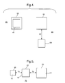
- Figure 3 depicts a detector aperture angularly and laterally aligned with an image of
an isolated area.
- Figure 4 illustrates positions of the detector for measurement of a stray radiation
parameter and a reference parameter.
- Figure 5 illustrates the use of a plurality of isolated areas.
- Figure 6 shows a determination of a stray radiation condition of a projection
system. Along the horizontal axis the position in the field is indicated, and along the
vertical axis the value of stray radiation coefficients is plotted.
Embodiment 1
-
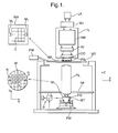
Figure 1 schematically depicts a lithographic proj ection apparatus
according to a particular embodiment of the invention. The apparatus comprises:
- a radiation system Ex, IL, for supplying a projection beam PB of radiation (e.g.
UV radiation such as for example generated by an excimer laser operating at a
wavelength of 248 nm, 193 nm or 157 nm, or by a laser-fired plasma source operating at
13,6 nm). In this particular case, the radiation system also comprises a radiation source
LA;
- a first object table (mask table) MT provided with a mask holder for holding a mask
MA (e.g. a reticle), and connected to first positioning means PM for accurately
positioning the mask with respect to item PL;
- a second object table (substrate table) WT provided with a substrate holder for
holding a substrate W (e.g. a resist-coated silicon wafer), and connected to second
positioning means PW for accurately positioning the substrate with respect to item PL;
and
- a projection system ("lens") PL (e.g. a quartz and/or CaF2 lens system or a
catadioptric system comprising lens elements made from such materials, or a mirror
system) for imaging an irradiated portion of the mask MA onto a target portion C (e.g.
comprising one or more dies) of the substrate W.
-
As here depicted, the apparatus is of a transmissive type (i.e. has a
transmissive mask). However, in general, it may also be of a reflective type, for example
(with a reflective mask). Alternatively, the apparatus may employ another kind of
patterning means, such as a programmable mirror array of a type as referred to above.
-
The source LA (e.g. a UV excimer laser, a laser-fired plasma source, a
discharge source, or an undulator or wiggler provided around the path of an electron
beam in a storage ring or synchrotron) produces a beam of radiation. This beam is fed
into an illumination system (illuminator) IL, either directly or after having traversed
conditioning means, such as a beam expander Ex, for example. The illuminator IL may
comprise adjusting means AM for setting the outer and/or inner radial extent (commonly
referred to as σ-outer and σ-inner, respectively) of the intensity distribution in the beam.
In addition, it will generally comprise various other components, such as an integrator IN
and a condenser CO. In this way, the beam PB impinging on the mask MA has a desired
uniformity and intensity distribution in its cross-section.
-
It should be noted with regard to figure 1 that the source LA may be
within the housing of the lithographic projection apparatus (as is often the case when the
source LA is a mercury lamp, for example), but that it may also be remote from the
lithographic projection apparatus, the radiation beam which it produces being led into the
apparatus (e.g. with the aid of suitable directing mirrors); this latter scenario is often the
case when the source LA is an excimer laser. The current invention and claims
encompass both of these scenarios.
-
The beam PB subsequently intercepts the mask MA, which is held on a
mask table MT. Having traversed the mask MA, the beam PB passes through the lens PL,
which focuses the beam PB onto a target portion C of the substrate W. With the aid of the
second positioning means PW (and interferometric measuring means IF), the substrate
table WT can be moved accurately, e.g. so as to position different target portions C in the
path of the beam PB. Similarly, the first positioning means PM can be used to accurately
position the mask MA with respect to the path of the beam PB, e.g. after mechanical
retrieval of the mask MA from a mask library, or during a scan. In general, movement of
the object tables MT, WT will be realized with the aid of a long-stroke module (coarse
positioning) and a short-stroke module (fine positioning), which are not explicitly
depicted in figure 1. However, in the case of a wafer stepper (as opposed to a step-and-scan
apparatus) the mask table MT may just be connected to a short stroke actuator, or
may be fixed. Mask MA and substrate W may be aligned using mask alignment marks
M1, M2 and substrate alignment marks P1, P2.
-
The depicted apparatus can be used in two different modes:
- 1. In step mode, the mask table MT is kept essentially stationary, and an entire mask
image is projected in one go (i.e. a single "flash") onto a target portion C. The substrate
table WT is then shifted in the x and/or y directions so that a different target portion C
can be irradiated by the beam PB; and
- 2. In scan mode, essentially the same scenario applies, except that a given target
portion C is not exposed in a single "flash". Instead, the mask table MT is movable in a
given direction (the so-called "scan direction", e.g. the y direction) with a speed v, so that
the projection beam PB is caused to scan over a mask image; concurrently, the substrate
table WT is simultaneously moved in the same or opposite direction at a speed V = Mv,
in which M is the magnification of the lens PL (typically, M = 1/4 or 1/5). In this manner,
a relatively large target portion C can be exposed, without having to compromise on
resolution.
-
-
A transmission image sensor TIS can be used to determine the lateral
position and best focus position (i.e. horizontal and vertical position) of the projected
image from the mask under the projection lens. A transmission image sensor TIS is inset
into a physical reference surface associated with the substrate table WT. In a particular
embodiment, two sensors are mounted on fiducial plates mounted to the top surface of the
substrate table WT, at diagonally opposite positions outside the area covered by the wafer
W. Each fiducial plate is made of a highly stable material with a very low coefficient of
thermal expansion, e.g. Invar, and has a flat reflective upper surface which may carry
markers used with another fiducial in alignment processes. The TIS is used to determine
directly the vertical (and horizontal) position of the aerial image of the projection lens. It
comprises apertures in the respective surface close behind which is placed a
photodetector sensitive to the radiation used for the exposure process.
-
To determine the position of the focal plane, the projection lens projects
into space an image of a pattern provided on the mask MA and having contrasting light
and dark regions. The substrate table is then scanned horizontally (in one or preferably
two directions) and vertically so that the aperture of the TIS passes through the space
where the aerial image is expected to be. As the TIS aperture passes through the light
and dark portions of the image of the TIS pattern, the output of the photodetector will
fluctuate (a Moiré effect). The vertical level at which the rate of change of amplitude of
the photodetector output is highest indicates the level at which the pattern image has the
greatest contrast, and hence indicates the plane of optimum focus. The horizontal level at
which the rate of change is highest indicates the aerial image's lateral position. An
example of a TIS of this type is described in greater detail in US 4,540,277, incorporated
herein by reference. Advantages of TIS include robustness and speed, because it is a
direct measurement technique not involving exposure of a resist.
-
According to the present embodiment, a spot sensor which is part of the
TIS is used, the spot sensor comprising a photodiode with an extremely small detection
area. However, any other suitable spot sensor, comprising a radiation sensor with small
detection area, could be used apart from sensors associated with TIS. One specific TIS
comprises a square detector aperture with dimensions 28 µm x 28 µm in front of a
photodiode.
-
In the present embodiment, the mean wavelength of the projection beam
is 248 nm, and the NA of a patterned beam impinging on the image plane is 0.7. Further,
the test pattern for measuring stray radiation comprises a square opaque area 10 with
sides 20 with a length SO, as illustrated in Figure 2. The opaque area is comprised within
a transmissive area 11. The geometrical image 30 of the opaque area is a square,
substantially unexposed area 31 comprised within an exposed area 32. The sides 33 of the
image of the opaque area 10 have a length SI given by the modulus value |M × SO|. For
example, with SO = 120 µm, and M = -0.25, we have SI = 30 µm. As shown in Figure 3
the shape of the square detector aperture of the TIS sensor, with sides 50 of a length SD
of 28 µm, is congruent to a notional shape having an edge 40 which is obtained from the
shape of the area 31 by displacing each line element constituting the shape of area 31,
parallel to itself, over a distance of 1 µm. Here, λ/NA is smaller than 1 µm: we have
λ/NA = 248/0.7 = 0.354 µm. So, when the detector aperture of the TIS is positioned such
that its edge 50 coincides with the edge 40, primarily stray radiation of a range greater
that 1 µm is detected with the TIS sensor. For clarity, in Figure 3 the edge 50 is
schematically shown in a position separated from the edge 40; during measurement of
stray radiation the edges 40 and 50 preferably substantially coincide. In that case the TIS
detector aperture is angularly aligned with respect to the opaque area 10, and centered
with respect to the image 30.
-
A measurement of a stray radiation condition of a projection system
involves at least two subsequent measurements, whereby the detector aperture with its
edge 50 is positioned in two different positions 60 and 61 with respect to the image of the
opaque area with sides 33, see Figure 4. In position 60, the above mentioned centered and
aligned position, stray radiation is measured, and the signal generated by the detector in
response to the impinging stray radiation is a stray radiation parameter S1. In position 61
the TIS sensor is irradiated directly by the projection beam; the detector signal S2 is the
reference parameter to be used for normalizing S1, such that a stray radiation coefficient
Co is obtained: Co = S1/S2. In first approximation the coefficient Co is representative for
stray radiation present in the range R given by R = [(1/2) × (SI -SD), infinity]; for the
present embodiment, the range is R = [1 µm, infinity]. Here, the term "infinity" is not to
be taken literally, but to be understood to indicate that at the long end the range of stray
radiation which can be detected is limited by the maximum size of a target portion that
can be irradiated by the projection beam.
-
The distance 62 between the sides 33 of the image of the isolated area and
the detector aperture 50 is indicated schematically by the arrow 62 in Figure 4. This
distance shall be much larger than the extent of the side 33, and such that the
measurement is to good approximation not affected by the presence of the substantially
unexposed area comprised by the sides 33.
Embodiment 2
-
In an embodiment of the invention the test pattern comprises a series 70 of
square, opaque isolated areas 10, with sides 20 of increasing length, as shown in Figure 5.
In this figure a series of three isolated areas is shown, which may for example be
embodied to have a side length of respectively 160 µm, 252 µm, and 400 µm.
-
According to the method of embodiment 1, stray radiation coefficients
Co1, Co2 and Co3 representative, in first approximation, for stray radiation in the ranges
R1 = [6 µm, infinity], R2 = [17.5 µm, infinity], and R3 = [36 µm, infinity] can be
determined. Preferably, the test pattern comprises a plurality of series 70 at a
corresponding plurality of positions in the field of the projection system, so that an
assessment of the stray radiation condition of the projection system for different field
positions can be made. Using the positioning means of the alignment system to
subsequently position the detector aperture of the TIS at measurement positions 60 and
61 as defined with respect to each image 50 of the isolated area of the series 70, a fast in
situ stray radiation condition determination is possible. The distance between the areas 10
is indicated schematically by the arrows 71 in Figure 5. This distance shall be much
larger than the extent of the sides 20 such that stray radiation measurements are not
affected by the presence of neighboring isolated areas.
-
In Figure 6 the result of such a determination is shown where the test
pattern comprised five series 70 of three opaque isolated areas, at five positions in the
field. The stray radiation coefficients Co1, Co2 and Co3 are plotted along the vertical
axis; the position in the field is plotted along the horizontal axis.
Embodiment 3
-
This embodiment is similar to the embodiment 1 save for the below. In
this embodiment the area 10 is transmissive, and the area 11 is opaque. The test pattern
also comprises a transmissive area of sufficient size to enable a reference measurement of
the projection beam radiation intensity in the absence of effects due to opaque areas. In
this area the detected signal is S2, as described in embodiment 1. The detected radiation
intensity 12 in this area is the sum of a notional intensity I21 which would be present in
the absence of stray radiation, and a contribution Isr due to stray radiation in a range Rref
= [0 µm, infinity] : this contribution Isr is denoted as Isr2[0 µm, infinity]
I2 = I21 + Isr2[0 µm, infinity].
Similarly, in position 60, the detected radiation intensity I1 (provided as a signal S1) is
the sum of said notional intensity I21 and a contribution Isr1[0 µm, (1/2) × (SI -SD) µm]
due to stray radiation in the range R1 = [0, (1/2) × (SI -SD) µm]. :
I1 = I21 + Isr1[0 µm, (1/2) × (SI -SD) µm].
The difference between the intensities I2 and I1 is given by
I2 - I1 = Isr2[0 µm, infinity] - Isr1[0 µm, (1/2) × (SI -SD) µm].
This difference is a measure for the stray radiation in the range R = [(1/2) × (SI -SD) µm
, infinity]; upon normalization by the reference parameter S2 a coefficient representative
of the stray radiation condition is obtained. So, in this embodiment of the method a stray
radiation coefficient Co representative for stray radiation in the range R = [(1/2) × (SI
- SD) µm, infinity] is obtained according to the formula Co = (S2 - S1)/S2 . It is an
alternative way to measure the same stray radiation coefficient as described in
embodiment 1.
Embodiment 4
-
A lithography projection apparatus provided with, for example, a
discharge source for providing a projection beam of radiation with a mean wavelength of
13,6 nm, is typically featuring a projection system PL embodied as a mirror system. For
determining a stray radiation condition of said mirror system it is not necessary that the
mean wavelength of the projection beam used for projecting the test pattern is also 13,6
nm. Since mirror systems are achromatic, i.e., the geometric optical imaging properties
are wavelength independent, the projection beam used for projecting the test pattern may
have any other mean wavelength, such as for example, a longer wavelength or a plurality
of longer wavelengths. This enables an even more extensive stray radiation condition
assessment of the projection system.
-
Whilst specific embodiments of the invention have been described above,
it will be appreciated that the invention may be practiced otherwise than as described.
The description is not intended to limit the invention.