EP1410143B1 - Prozessor mit geschütztem prüfungs- und fehlerbeseitigungsmodus - Google Patents
Prozessor mit geschütztem prüfungs- und fehlerbeseitigungsmodus Download PDFInfo
- Publication number
- EP1410143B1 EP1410143B1 EP02719514A EP02719514A EP1410143B1 EP 1410143 B1 EP1410143 B1 EP 1410143B1 EP 02719514 A EP02719514 A EP 02719514A EP 02719514 A EP02719514 A EP 02719514A EP 1410143 B1 EP1410143 B1 EP 1410143B1
- Authority
- EP
- European Patent Office
- Prior art keywords
- hdt
- control logic
- register
- mode
- processor
- Prior art date
- Legal status (The legal status is an assumption and is not a legal conclusion. Google has not performed a legal analysis and makes no representation as to the accuracy of the status listed.)
- Expired - Lifetime
Links
Images


Classifications
-
- G—PHYSICS
- G06—COMPUTING OR CALCULATING; COUNTING
- G06F—ELECTRIC DIGITAL DATA PROCESSING
- G06F9/00—Arrangements for program control, e.g. control units
- G06F9/06—Arrangements for program control, e.g. control units using stored programs, i.e. using an internal store of processing equipment to receive or retain programs
- G06F9/22—Microcontrol or microprogram arrangements
- G06F9/24—Loading of the microprogram
-
- G—PHYSICS
- G06—COMPUTING OR CALCULATING; COUNTING
- G06F—ELECTRIC DIGITAL DATA PROCESSING
- G06F1/00—Details not covered by groups G06F3/00 - G06F13/00 and G06F21/00
Definitions
- This invention relates generally to computing systems, and, more particularly, to a method and apparatus for protecting personal computer systems from unauthorized back door accesses.
- Fig. 1 illustrates an exemplary computer system 100.
- the computer system 100 includes a processor 102, a north bridge 104, memory 106, Advanced Graphics Port (AGP) memory 108, a Peripheral Component Interconnect (PCI) bus 110, a south bridge 112, a battery, an AT Attachment (ATA) interface 114 (more commonly known as an Integrated Drive Electronics (IDE) interface), a universal serial bus (USB) interface 116, a Low Pin Count (LPC) bus 118, an input/output controller chip (SuperI/OTM) 120, and BIOS memory 122.
- ATA AT Attachment
- USB Universal Serial Bus
- LPC Low Pin Count
- SuperI/OTM input/output controller chip
- north bridge 104 and the south bridge 112 may include only a single chip or a plurality of chips, leading to the collective term "chipset.” It is also noted that other buses, devices, and/or subsystems may be included in the computer system 100 as desired, e.g. caches, modems, parallel or serial interfaces, SCSI interfaces, network interface cards, etc. ["SuperI/O” is a trademark of National Semiconductor Corporation of Santa Clara, Calif.]
- the processor 102 is coupled to the north bridge 104.
- the north bridge 104 provides an interface between the processor 102, the memory 106, the AGP memory 108, and the PCI bus 110.
- the south bridge 112 provides an interface between the PCI bus 110 and the peripherals, devices, and subsystems coupled to the IDE interface 114, the USB interface 116, and the LPC bus 118.
- the battery 113 is shown coupled to the south bridge 112.
- the Super I/OTM chip 120 is coupled to the LPC bus 118.
- the north bridge 104 provides communications access between and/or among the processor 102, memory 106, the AGP memory 108, devices coupled to the PCI bus 110, and devices and subsystems coupled to the south bridge 112.
- removable peripheral devices are inserted into PCl "slots" (not shown) that connect to the PCI bus 110 to couple to the computer system 100.
- PCl slots not shown
- devices located on a motherboard may be directly connected to the PCI bus 110.
- the south bridge 112 provides an interface between the PCI bus 110 and various devices and subsystems, such as a modem, a printer, keyboard, mouse, etc., which are generally coupled to the computer system 100 through the LPC bus 118 (or its predecessors, such as an X-bus or an ISA bus).
- the south bridge 112 includes the logic used to interface the devices to the rest of computer system 100 through the IDE interface 114, the USB interface 116, and the LPC bus 118.
- Initializing registers with default values after a processor reset is a known technique. Such a technique is disclosed in 'intel 82802 AB/82802 AC Firmware Hub' Datasheet published by intel on 30 November 2000.
- an x86 operating environment provides little for protecting user privacy, providing security for corporate secrets and assets, or protecting the ownership rights of content providers. All of these goals, privacy, security, and ownership (collectively, PSO) are becoming critical in an age of Internet-connected computers. The original personal computers were not designed in anticipation of PSO needs.
- a processor in accordance with the present invention, includes a first register configured to store one or more hardware-debug-test (HDT) enable bits, a first control logic coupled to receive a plurality of HDT input signals, and a second control logic coupled to the first register.
- the first control logic is coupled to access the first register.
- the second control logic is configured to store one or more default values in the first register in response to a reset of the processor.
- the processor is characterized in that when the processor is in a system management mode and the HDT enable status bits indicate HDT mode is disabled, a predetermined input into HDT control logic changes the HDT mode to enabled.
- a method for determining an HDT mode enable status includes receiving a request to initiate the HDT mode, determining HDT mode enable status, initiating the HDT mode if the HDT mode enable status is set to enabled, characterized in that when a processor is in system management mode and the HDT status enable bits indicate HDT is disabled, the method includes providing a predetermined input into HDT control logic which changes the HDT mode to enabled.
- SMM System Management Mode
- Fig. 2 illustrates a block diagram of an embodiment of a flowchart showing data and command flow in a computer system having a secure execution box 260, according to one aspect of the present invention.
- User input and output (I/O) data and/or commands 205 are provided to and received from one or more applications 210.
- the applications 210 exchange data and commands with cryptography service providers 215 within the computer system, such as the computer system 100 or any other computer system.
- the cryptography service providers 215 may use API (Application Programming Interface) calls 220 to interact with drivers 225 that provide access to hardware 230.
- API Application Programming Interface
- the drivers 225 and the hardware 230 are part of a secure execution box configured to operate in a secure execution mode (SEM) 260.
- SEM secure execution mode
- PSO Trusted privacy, security and ownership
- SMM secure execution box
- security operations also referred to simply as security operations, may take place while the computer system is in SEM 260.
- Software calls propagated from the user I/O 205 and/or the applications 210 may be placed into the secure execution box in SMM 260. The software calls have access to the secure execution box in SEM 260 to various security hardware resources.
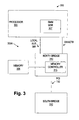
- Fig. 3 illustrates a block diagram of an embodiment of a computer systems 300 with SMM MSRs, according to various aspects of the present invention.
- Fig. 3 includes a processor 305, a north bridge 310, memory 306, and a south bridge 330.
- the processor includes one or more SMM MSRs (machine specific registers) 307.
- the north bridge 310 includes a memory controller 315.
- the north bridge 310 is coupled between the processor 305 and the south bridge 330, to the processor 305 through a local bus 308 and to the south bridge 330 through the PCI bus 110.
- the north bridge 310 is coupled to receive the SMIACT# signal from the processor 305.
- the computer system 300 signals that the processor 305 is in SMM using standard processor signals (e.g. SMIACT# to the north bridge 310) and/or bus cycles on the local bus 308 and PCI bus 110.
- standard processor signals e.g. SMIACT# to the north bridge 310
- bus cycles on the local bus 308 and PCI bus 110.
- the security of SMM is assumed. It is noted that one or more so-called "backdoors" may exist that could be exploited to compromise the security of SMM.
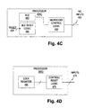
- the issues contemplated include misuse of the hardware debug test (HDT) mode of the processor 305 as well as the ability of the processor 305 to load and replace microcode. Illustrated in Figs. 4A-D are various embodiments 305A, 305B, 305C, 305D of the processor 305, each of which includes various security protections against one or more backdoor attacks.
- the processor 305A includes HDT control logic 410A, HDT reset logic 420A, and one or more registers, including an HDT enable register 415 and non-volatile random access memory (NVRAM) 430.
- the HDT control logic 410A is coupled to receive a plurality of input signals through a plurality of HDT pins 405.
- the HDT control logic 410A is further coupled to the HDT enable register 415.
- the HDT reset logic 420A is coupled to receive a RESET signal over a line 425 and to access (i.e. read and write) the HDT enable register 415 and the NVRAM 430.
- the processor 305B of Fig. 4B includes HDT control logic 410B, HDT reset logic 420B, and two registers, including the HDT enable register 415 and an HDT enable lock register 435.
- the HDT control logic 410B is coupled to receive a plurality of input signals through the plurality of HDT pins 405.
- the HDT control logic 410B is further coupled to the HDT enable register 415 and the HDT enable lock register 435.
- the HDT reset logic 420B is coupled to receive the RESET signal over the line 425 and a signal, such as over a line 440, through a pull-up (or pull-down) resistor 445.
- the processor 305C includes microcode control logic 455, microcode loader enable reset logic 465, and one or more registers, including a microcode loader enable register 460.
- the microcode control logic 455 is coupled to receive a plurality of input signals through a plurality of microcode input pins 450.
- the microcode control logic 455 is further coupled to the microcode loader enable register 460.
- the microcode loader enable reset logic 465 is coupled to receive the RESET signal and to access the microcode loader enable register 460.
- the processor 305D includes HDT control logic 410 integrated with the microcode control logic 455, the HDT reset logic 420, and the MLE reset logic 465 to form control/reset logic 475.
- the HDT enable register 415 and the microcode loader enable register 460 are integrated into a multibit lock register 480.
- a plurality of inputs 470 are shown to the control/reset logic 475.
- the plurality of inputs 470 may include the HDT inputs 405, the microcode inputs 450, and/or the reset signaling means.
- Other embodiments integrate only the HDT control logic 410 and the microcode control logic 455, or just the HDT reset logic 420 and the MLE reset logic 465.
- the registers 415, 435, and 460, as well as the NVRAM 430 include storage space for one or more bits.
- each register is configured to store a single bit.
- the enable registers 415 and 460 may also be integrated into a single lock register, and the HDT enable lock register 435 may be used as a microcode enable lock register. It is contemplated that the registers 415, 435, 460, and/or 480 could be included in the SMM MSRs 307.
- the HDT enable register 415 is configured to store one or more HDT enable bits signifying whether HDT mode is enabled or disabled.
- the HDT reset logic 420 is configured to set the one or more HDT enable bits to a default state upon a reset of the processor 305.
- the HDT mode is enabled as the default on non-production processors 305 used for engineering and testing.
- the HDT mode may be disabled as the default in standard production processors 305.
- the default state may be stored in and read from the NVRAM 430.
- the default state may be changeable, but in the illustrated embodiment, the default state is set to disabled.
- the default state is set using a strapping option. The default value is provided to the HDT reset logic 420B through the pull-up (or pull-down) resistor 445.
- the microcode update mode is enabled as the default on non-production processors 305 used for engineering and testing.
- the microcode update mode may be disabled as the default in standard production processors 305.
- the default state may be stored in and read from the NVRAM 430.
- the default state may be changeable, but in the illustrated embodiment the default state is set to disabled.
- the default state is using a strapping option. The default value is provided to the MLE reset logic 465 through the pull-up (or pull-down) resistor 445.
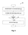
- a method 500 for initiating the HDT mode is shown.
- the HDT control logic 410 checks the status of the one or more HDT enable bits to see if the HDT mode is enabled or disabled (step 510). If the HDT mode is enabled (step 515), then the HDT control logic 410 initiates the HDT mode (step 520). If the HDT mode is disabled (step 515), then the HDT control logic 410 will not initiate the HDT mode.
- a method 600 for changing the HDT mode enable status which includes an HDT mode lock
- the HDT control logic 410 checks the status of the one or more HDT enable lock bits to determine if the HDT lock mode is locked or unlocked (step 610). If the HDT lock mode is unlocked (step 615), then the HDT control logic 410 initiates HDT mode (step 635). If the HDT lock mode is locked (step 615), then the HDT control logic 410 requests authorization to change the HDT lock mode status (step 620). If the change is authorized (step 625), then the HDT control logic 410 changes the HDT mode lock bit to unlocked (step 630). If the change is not authorized (step 625), then the HDT control logic 410 does not change the HDT mode lock bit.
- the HDT enable status may be changed by setting or resetting the one or more HDT enable status bits.
- the HDT mode may be disabled, but inside SMM, a predetermined input to the HDT control logic 410 may signal the HDT control logic 410 to change the HDT mode status to enabled.
- the HDT control logic 410 would change the status of the HDT enable bit from disabled to enabled.
- the HDT control logic 410 checks the status of the one or more HDT enable lock bits to see if the HDT lock mode is enabled or disabled. If the HDT lock mode is disabled, then the HDT control logic 410 may change the HDT mode status. If the HDT lock mode is enabled, then the HDT control logic 410 will not change the HDT mode status.
- the method 600 may alternatively terminate if the HDT lock mode is locked (step 615), instead of requesting authorization to change the HDT lock mode status (step 620).
- the method 600 may also include receiving a request to change the HDT lock mode status (not shown) prior to the method 600 requesting authorization (step 620).
- a method 700 for initiating the microcode loader is shown.
- the microcode control logic 455 checks the status of the one or more microcode enable bits to see if microcode update mode is enabled or disabled (step 710). If the microcode update mode is enabled (step 715), then the microcode control logic 455 initiates the microcode update mode (step 720). If the microcode update mode is disabled (step 715), then the microcode control logic 455 will not initiate the microcode update mode.
- a method 800 for changing the microcode update mode enable status which includes a microcode mode lock
- the microcode control logic 455 checks the status of the one or more microcode enable lock bits to see if the microcode mode is locked or unlocked (step 810). If the microcode lock mode is unlocked (step 815), then the microcode control logic 455 initiates the microcode mode (step 835). If the microcode lock mode is locked (step 815), then the microcode control logic 455 requests authorization to change the microcode mode lock status (step 820). If the change is authorized (step 825), then the microcode control logic 455 changes the microcode mode lock bit to unlocked (step 830). If the change is not authorized (step 825), then the microcode control logic 455 does not change the microcode mode lock bit.
- the microcode enable status may be changed by setting or resetting the one or more microcode enable status bits.
- the microcode mode may be disabled, but inside SMM, a predetermined input to the microcode control logic 455 may signal the microcode control logic 455 to change the microcode mode status to enabled.
- the microcode control logic 455 will change the status of the one or more microcode enable bits from disabled to enabled.
- the microcode control logic 455 may check the status of the one or more microcode enable lock bits to determine if the microcode lock mode is enabled or disabled. If the microcode lock mode is disabled, then the microcode control logic 455 may change the microcode mode status. If the microcode lock mode is enabled, then the microcode control logic 455 will not change the microcode mode status.
- the method 800 may alternatively terminate if the microcode update lock status is locked (step 815), instead of requesting authorization to change the microcode update lock status (step 820).
- the method 800 may also include receiving a request to change the microcode update lock status (not shown) prior to the method 3500 requesting authorization (step 820).
- references to ROM are to be construed as also applying to flash memory and other substantially non-volatile memory types.
- ROM read-only memory
- references to ROM are to be construed as also applying to flash memory and other substantially non-volatile memory types.
- the software-implemented aspects of the invention are typically encoded on some form of program storage medium or implemented over some type of transmission medium.
- the program storage medium may be magnetic e.g., a floppy disk or a hard drive) or optical ( e.g., a compact disk read only memory, or "CD ROM"), and may be read only or random access.
- the transmission medium may be twisted wire pairs, coaxial cable, optical fiber, or some other suitable transmission medium known to the art. The invention is not limited by these aspects of any given implementation.
Landscapes
- Engineering & Computer Science (AREA)
- Theoretical Computer Science (AREA)
- Software Systems (AREA)
- Physics & Mathematics (AREA)
- General Engineering & Computer Science (AREA)
- General Physics & Mathematics (AREA)
- Storage Device Security (AREA)
- Test And Diagnosis Of Digital Computers (AREA)
- Stored Programmes (AREA)
- Executing Machine-Instructions (AREA)
- Debugging And Monitoring (AREA)
Claims (10)
- Prozessor mit:dadurch gekennzeichnet, daß, wenn sich der Prozessor (305) in einem System-Management-Modus befindet und die HDT-Freigabezustandsbits angeben, daß der HDT-Modus deaktiviert ist, ein vorbestimmtes Eingangssignal in die HDT-Steuerlogik (410) den HDT-Modus in den aktivierten Zustand ändert.einem ersten Register (415), das zum Speichern von einem oder mehreren Hardware-Debug-Test(HDT)-Freigabebits ausgebildet ist;einer ersten Steuerlogik (410), die zum Empfangen mehrerer HDT-Eingangssignale gekoppelt ist, wobei die erste Steuerlogik zum Zugriff auf das erste Register gekoppelt ist; undeiner mit dem ersten Register gekoppelten zweiten Steuerlogik (420), wobei die zweite Steuerlogik ausgebildet ist, um in Reaktion auf das Rücksetzen eines Prozessors einen oder mehrere Voreinstellungswerte im ersten Register zu speichern,
- Prozessor nach Anspruch 1, bei dem die erste Steuerlogik ferner dazu ausgebildet ist, eine Anforderung zum Eintritt in einen HDT-Modus zu empfangen, wobei die erste Steuerlogik ferner derart ausgebildet ist, ausgewählte Einträge des einen oder der mehreren, in dem ersten Register gespeicherten HDT-Freigabebits in Reaktion auf die Anforderung nach dem Eintritt in den HDT-Modus zu lesen, und wobei die erste Steuerlogik ferner derart ausgebildet ist, daß sie die Anforderung nach dem Eintritt in den HDT-Modus basierend auf den ausgewählten Einträgen des einen oder der mehreren HDT-Freigabebits gewährt oder ablehnt.
- Prozessor nach Anspruch 1, ferner mit:einer oder mehreren nicht-flüchtigen Speicherzellen, die zum Speichern des einen oder der mehreren Voreinstellungswerte für das eine oder die mehreren HDT-Freigabebits ausgebildet sind, wobei die zweite Steuerlogik ferner verbunden ist, um den einen oder die mehreren Voreinstellungswerte für das eine oder die mehreren HDT-Freigabebits aus der einen oder den mehreren nicht-flüchtigen Speicherzellen zu lesen und den einen oder die mehreren Voreinstellungswerte für das eine oder die mehreren HDT-Freigabebits in Reaktion auf das Rücksetzen des Prozessors in das erste Register zu schreiben.
- Prozessor nach Anspruch 1, bei dem die zweite Steuerlogik ferner verbunden ist, um ein Signal zu empfangen, das den einen oder die mehreren Voreinstellungswerte für das eine oder die mehreren HDT-Freigabebits angibt, und um den einen oder die mehreren Voreinstellungswerte für das eine oder die mehreren HDT-Freigabebits in Reaktion auf das Rücksetzen des Prozessors in das erste Register zu schreiben.
- Prozessor nach Anspruch 1, ferner mit:einem dritten Register, das zum Speichern eines oder mehrerer Mikrocode-Ladeeinrichtung-Freigabebits ausgebildet ist;einer dritten Steuerlogik, die zum Empfangen mehrerer Mikrocodeeingänge verbunden ist, wobei die dritte Steuerlogik zum Zugreifen auf das dritte Register verbunden ist; undeiner vierten Steuerlogik, die mit dem dritten Register verbunden ist, wobei die vierte Steuerlogik derart ausgebildet ist, daß sie in Reaktion auf das Rücksetzen des Prozessors einen oder mehrere Voreinstellungswerte im dritten Register speichert.
- Prozessor nach Anspruch 5, bei dem die dritte Steuerlogik ferner derart ausgebildet ist, daß sie eine Anforderung zur Veränderung des Mikrocodes empfängt, wobei die dritte Steuerlogik ferner derart ausgebildet ist, daß sie ausgewählte Einträge des einen oder der mehreren, in dem dritten Register gespeicherten Mikrocode-Ladeeinrichtung-Freigabebits in Reaktion auf die Anforderung nach einer Veränderung des Mikrocodes liest, und wobei die dritte Steuerlogik ferner derart ausgebildet ist, daß sie die Anforderung nach einer Veränderung des Mikrocodes basierend auf den ausgewählten Einträgen des einen oder der mehreren Mikrocode-Ladeeinrichtung-Freigabebits gewährt oder ablehnt.
- Prozessor nach Anspruch 1, ferner mit:einem mit der ersten Steuerlogik verbundenen zweiten Register, wobei das zweite Register zum Speichern eines oder mehrerer HDT-Freigabe-Sperrbits ausgebildet ist.
- Prozessor nach Anspruch 7, bei dem die erste Steuerlogik ferner zum Empfangen einer Anforderung nach einer Veränderung des HDT-Modus-Status ausgebildet ist, wobei die erste Steuerlogik ferner derart ausgebildet ist, daß sie ausgewählte Einträge des einen oder der mehreren, in dem zweiten Register gespeicherten HDT-Freigabe-Sperrbits in Reaktion auf die Anforderung nach einer Veränderung des HDT-Modus-Status liest, und wobei die erste Steuerlogik ferner derart ausgebildet ist, daß sie die Anforderung nach einer Veränderung des HDT-Modus-Status basierend auf den ausgewählten Einträgen des einen oder der mehreren HDT-Freigabe-Sperrbits gewährt oder ablehnt.
- Verfahren zum Bestimmen eines HDT-Modus-Freigabestatus, wobei das Verfahren umfaßt:dadurch gekennzeichnet, daß, wenn ein Prozessor (305) sich im System-Management-Modus befindet und die HDT-Freigabestatusbits HDT als deaktiviert angeben, das Verfahren das Liefern eines vorbestimmten Eingangssignals an die HDT-Eingangslogik (410) vorsieht, welches den HDT-Modus aktiviert.Empfangen einer Anforderung zum Initiieren des HDT-Modus;Bestimmen des HDT-Modus-Status;Initiieren des HDT-Modus, wenn der HDT-Modus-Freigabestatus aktiviert ist,
- Verfahren nach Anspruch 9, bei dem das Bestimmen des HDT-Modus-Freigabestatus das Lesen eines oder mehrerer Einträge aus einem Register umfaßt, die einem oder mehreren HDT-Freigabebits entsprechen.
Applications Claiming Priority (7)
| Application Number | Priority Date | Filing Date | Title |
|---|---|---|---|
| US852372 | 1992-03-13 | ||
| US852942 | 1997-05-08 | ||
| US85294201A | 2001-05-10 | 2001-05-10 | |
| US09/852,372 US7065654B1 (en) | 2001-05-10 | 2001-05-10 | Secure execution box |
| US853226 | 2001-05-11 | ||
| US09/853,226 US20030028781A1 (en) | 2001-05-10 | 2001-05-11 | Mechanism for closing back door access mechanisms in personal computer systems |
| PCT/US2002/011935 WO2002093336A2 (en) | 2001-05-10 | 2002-04-17 | Processor with protected test and debug mode |
Publications (2)
| Publication Number | Publication Date |
|---|---|
| EP1410143A2 EP1410143A2 (de) | 2004-04-21 |
| EP1410143B1 true EP1410143B1 (de) | 2005-10-26 |
Family
ID=27420360
Family Applications (1)
| Application Number | Title | Priority Date | Filing Date |
|---|---|---|---|
| EP02719514A Expired - Lifetime EP1410143B1 (de) | 2001-05-10 | 2002-04-17 | Prozessor mit geschütztem prüfungs- und fehlerbeseitigungsmodus |
Country Status (9)
| Country | Link |
|---|---|
| US (1) | US20030028781A1 (de) |
| EP (1) | EP1410143B1 (de) |
| JP (1) | JP2005501313A (de) |
| KR (1) | KR20030094396A (de) |
| CN (1) | CN1520537A (de) |
| AU (1) | AU2002250591A1 (de) |
| DE (1) | DE60206924T2 (de) |
| TW (1) | TWI228889B (de) |
| WO (1) | WO2002093336A2 (de) |
Families Citing this family (25)
| Publication number | Priority date | Publication date | Assignee | Title |
|---|---|---|---|---|
| US20030097587A1 (en) * | 2001-11-01 | 2003-05-22 | Gulick Dale E. | Hardware interlock mechanism using a watchdog timer |
| US20040034872A1 (en) * | 2002-08-16 | 2004-02-19 | Peter Huyge | Method for triggering an event in an electronic device, and corresponding device |
| US7334123B2 (en) * | 2003-05-02 | 2008-02-19 | Advanced Micro Devices, Inc. | Computer system including a bus bridge for connection to a security services processor |
| BRPI0406198A (pt) * | 2003-07-28 | 2005-08-09 | Sony Corp | Aparelho e método de processamento de informação, meio de gravação gravando um programa legìvel por um computador, e, programa para fazer um computador executar um processo |
| US7805614B2 (en) * | 2004-04-26 | 2010-09-28 | Northrop Grumman Corporation | Secure local or remote biometric(s) identity and privilege (BIOTOKEN) |
| US7552341B2 (en) * | 2004-09-01 | 2009-06-23 | Microsoft Corporation | Licensing the use of software on a particular CPU |
| JP4309361B2 (ja) * | 2005-03-14 | 2009-08-05 | パナソニック株式会社 | 電子機器制御システム及び制御信号送信装置 |
| JP4207050B2 (ja) * | 2005-06-27 | 2009-01-14 | コニカミノルタビジネステクノロジーズ株式会社 | 画像形成装置 |
| US7925815B1 (en) * | 2006-06-29 | 2011-04-12 | David Dunn | Modifications to increase computer system security |
| US8661265B1 (en) | 2006-06-29 | 2014-02-25 | David Dunn | Processor modifications to increase computer system security |
| US7610426B1 (en) * | 2006-12-22 | 2009-10-27 | Dunn David A | System management mode code modifications to increase computer system security |
| US8316414B2 (en) * | 2006-12-29 | 2012-11-20 | Intel Corporation | Reconfiguring a secure system |
| US20090109984A1 (en) * | 2007-10-31 | 2009-04-30 | Dell Products L.P. | Wireless device with flash cache and boot from dock |
| US9286232B2 (en) * | 2009-01-26 | 2016-03-15 | International Business Machines Corporation | Administering registered virtual addresses in a hybrid computing environment including maintaining a cache of ranges of currently registered virtual addresses |
| US20120117227A1 (en) * | 2010-11-10 | 2012-05-10 | Sony Corporation | Method and apparatus for obtaining feedback from a device |
| US20120185688A1 (en) * | 2011-01-13 | 2012-07-19 | Google Inc. | Processor mode locking |
| CN105788638A (zh) * | 2011-03-04 | 2016-07-20 | 瑞萨电子株式会社 | 半导体器件 |
| CN103984908B (zh) * | 2014-05-05 | 2017-03-08 | 上海新储集成电路有限公司 | 一种南桥芯片及其应用方法 |
| US10101928B2 (en) * | 2016-02-19 | 2018-10-16 | Dell Products L.P. | System and method for enhanced security and update of SMM to prevent malware injection |
| US10534936B2 (en) * | 2017-08-30 | 2020-01-14 | Dell Products, Lp | System and method for enabling and disabling of baseboard management controller configuration lockdown |
| US11354406B2 (en) | 2018-06-28 | 2022-06-07 | Intel Corporation | Physics-based approach for attack detection and localization in closed-loop controls for autonomous vehicles |
| TWI682301B (zh) * | 2018-11-19 | 2020-01-11 | 歐生全科技股份有限公司 | 多功能認證裝置與運作方法 |
| NO346155B1 (en) * | 2020-10-26 | 2022-03-28 | Kongsberg Defence & Aerospace As | Configuration authentication prior to enabling activation of a FPGA having volatile configuration-memory |
| US12292975B2 (en) * | 2022-03-28 | 2025-05-06 | Intel Corporation | Method, system and apparatus to prevent denial of service attacks on PCIe based computing devices |
| US12164348B2 (en) * | 2022-10-04 | 2024-12-10 | Nxp Usa, Inc. | Capturing of on-chip resets in an integrated circuit |
Family Cites Families (4)
| Publication number | Priority date | Publication date | Assignee | Title |
|---|---|---|---|---|
| JPH0855023A (ja) * | 1994-07-25 | 1996-02-27 | Motorola Inc | データ処理システムおよびその方法 |
| JP3461234B2 (ja) * | 1996-01-22 | 2003-10-27 | 株式会社東芝 | データ保護回路 |
| US6154819A (en) * | 1998-05-11 | 2000-11-28 | Intel Corporation | Apparatus and method using volatile lock and lock-down registers and for protecting memory blocks |
| US6026016A (en) * | 1998-05-11 | 2000-02-15 | Intel Corporation | Methods and apparatus for hardware block locking in a nonvolatile memory |
-
2001
- 2001-05-11 US US09/853,226 patent/US20030028781A1/en not_active Abandoned
-
2002
- 2002-04-17 EP EP02719514A patent/EP1410143B1/de not_active Expired - Lifetime
- 2002-04-17 DE DE60206924T patent/DE60206924T2/de not_active Expired - Fee Related
- 2002-04-17 JP JP2002589946A patent/JP2005501313A/ja active Pending
- 2002-04-17 KR KR10-2003-7014546A patent/KR20030094396A/ko not_active Withdrawn
- 2002-04-17 AU AU2002250591A patent/AU2002250591A1/en not_active Abandoned
- 2002-04-17 CN CNA028124928A patent/CN1520537A/zh active Pending
- 2002-04-17 WO PCT/US2002/011935 patent/WO2002093336A2/en not_active Ceased
- 2002-04-26 TW TW091108639A patent/TWI228889B/zh not_active IP Right Cessation
Also Published As
| Publication number | Publication date |
|---|---|
| DE60206924T2 (de) | 2006-07-27 |
| AU2002250591A1 (en) | 2002-11-25 |
| WO2002093336A3 (en) | 2004-02-12 |
| WO2002093336A2 (en) | 2002-11-21 |
| JP2005501313A (ja) | 2005-01-13 |
| US20030028781A1 (en) | 2003-02-06 |
| KR20030094396A (ko) | 2003-12-11 |
| EP1410143A2 (de) | 2004-04-21 |
| TWI228889B (en) | 2005-03-01 |
| DE60206924D1 (de) | 2005-12-01 |
| CN1520537A (zh) | 2004-08-11 |
Similar Documents
| Publication | Publication Date | Title |
|---|---|---|
| EP1410143B1 (de) | Prozessor mit geschütztem prüfungs- und fehlerbeseitigungsmodus | |
| US7149854B2 (en) | External locking mechanism for personal computer memory locations | |
| US6795905B1 (en) | Controlling accesses to isolated memory using a memory controller for isolated execution | |
| US8533777B2 (en) | Mechanism to determine trust of out-of-band management agents | |
| JP3713141B2 (ja) | プログラムの不正実行防止方法 | |
| US6832317B1 (en) | Personal computer security mechanism | |
| JP4822646B2 (ja) | 分離実行環境で使用するためのキー階層の生成 | |
| US7107460B2 (en) | Method and system for securing enablement access to a data security device | |
| US6823451B1 (en) | Integrated circuit for security and manageability | |
| US7003676B1 (en) | Locking mechanism override and disable for personal computer ROM access protection | |
| US7085935B1 (en) | Managing a secure environment using a chipset in isolated execution mode | |
| EP0979460A1 (de) | System zur zugriffskontrolle zu einem register aufgenommen im addressenbereich eines rechnersystems | |
| US7194634B2 (en) | Attestation key memory device and bus | |
| MXPA02008913A (es) | Sistema y metodo para conectar un dispositivo de conducto serial universal a un sistema de computadora anfitrion. | |
| CN101625674B (zh) | 具有特别模块寄存器的微处理器及存取保护方法 | |
| US6968460B1 (en) | Cryptographic randomness register for computer system security | |
| US7007300B1 (en) | Secure booting of a personal computer system | |
| US7013481B1 (en) | Attestation key memory device and bus | |
| JP2004504663A (ja) | 分離実行環境での複数の分離メモリへのアクセスの制御 | |
| US6542995B2 (en) | Apparatus and method for maintaining secured access to relocated plug and play peripheral devices | |
| JP2005521941A (ja) | コンパートメント化されたセキュリティのための入出力許可ビットマップ | |
| US7216362B1 (en) | Enhanced security and manageability using secure storage in a personal computer system | |
| US6754815B1 (en) | Method and system for scrubbing an isolated area of memory after reset of a processor operating in isolated execution mode if a cleanup flag is set | |
| US7089418B1 (en) | Managing accesses in a processor for isolated execution | |
| US7111176B1 (en) | Generating isolated bus cycles for isolated execution |
Legal Events
| Date | Code | Title | Description |
|---|---|---|---|
| PUAI | Public reference made under article 153(3) epc to a published international application that has entered the european phase |
Free format text: ORIGINAL CODE: 0009012 |
|
| AK | Designated contracting states |
Kind code of ref document: A2 Designated state(s): AT BE CH CY DE DK ES FI FR GB GR IE IT LI LU MC NL PT SE TR |
|
| AX | Request for extension of the european patent |
Extension state: AL LT LV MK RO SI |
|
| 17P | Request for examination filed |
Effective date: 20031105 |
|
| 17Q | First examination report despatched |
Effective date: 20050215 |
|
| GRAP | Despatch of communication of intention to grant a patent |
Free format text: ORIGINAL CODE: EPIDOSNIGR1 |
|
| GRAS | Grant fee paid |
Free format text: ORIGINAL CODE: EPIDOSNIGR3 |
|
| GRAA | (expected) grant |
Free format text: ORIGINAL CODE: 0009210 |
|
| AK | Designated contracting states |
Kind code of ref document: B1 Designated state(s): DE GB |
|
| REG | Reference to a national code |
Ref country code: GB Ref legal event code: FG4D |
|
| REF | Corresponds to: |
Ref document number: 60206924 Country of ref document: DE Date of ref document: 20051201 Kind code of ref document: P |
|
| PGFP | Annual fee paid to national office [announced via postgrant information from national office to epo] |
Ref country code: GB Payment date: 20060314 Year of fee payment: 5 |
|
| PGFP | Annual fee paid to national office [announced via postgrant information from national office to epo] |
Ref country code: DE Payment date: 20060428 Year of fee payment: 5 |
|
| PLBE | No opposition filed within time limit |
Free format text: ORIGINAL CODE: 0009261 |
|
| STAA | Information on the status of an ep patent application or granted ep patent |
Free format text: STATUS: NO OPPOSITION FILED WITHIN TIME LIMIT |
|
| 26N | No opposition filed |
Effective date: 20060727 |
|
| GBPC | Gb: european patent ceased through non-payment of renewal fee |
Effective date: 20070417 |
|
| PG25 | Lapsed in a contracting state [announced via postgrant information from national office to epo] |
Ref country code: DE Free format text: LAPSE BECAUSE OF NON-PAYMENT OF DUE FEES Effective date: 20071101 |
|
| PG25 | Lapsed in a contracting state [announced via postgrant information from national office to epo] |
Ref country code: GB Free format text: LAPSE BECAUSE OF NON-PAYMENT OF DUE FEES Effective date: 20070417 |