EP1408552A1 - Integrated MOS semiconductor device with high performance and process of manufacturing the same - Google Patents
Integrated MOS semiconductor device with high performance and process of manufacturing the same Download PDFInfo
- Publication number
- EP1408552A1 EP1408552A1 EP20020425611 EP02425611A EP1408552A1 EP 1408552 A1 EP1408552 A1 EP 1408552A1 EP 20020425611 EP20020425611 EP 20020425611 EP 02425611 A EP02425611 A EP 02425611A EP 1408552 A1 EP1408552 A1 EP 1408552A1
- Authority
- EP
- European Patent Office
- Prior art keywords
- metal
- stripes
- metal stripes
- zones
- prolongation
- Prior art date
- Legal status (The legal status is an assumption and is not a legal conclusion. Google has not performed a legal analysis and makes no representation as to the accuracy of the status listed.)
- Withdrawn
Links
- 239000004065 semiconductor Substances 0.000 title claims abstract 18
- 238000000034 method Methods 0.000 title claims abstract 8
- 238000004519 manufacturing process Methods 0.000 title claims abstract 3
- 239000002184 metal Substances 0.000 claims abstract 58
- 239000000463 material Substances 0.000 claims abstract 28
- 239000004020 conductor Substances 0.000 claims abstract 24
- 238000000926 separation method Methods 0.000 claims abstract 16
- 230000015572 biosynthetic process Effects 0.000 claims abstract 12
- 239000000758 substrate Substances 0.000 claims abstract 12
- 238000000151 deposition Methods 0.000 claims abstract 6
- 230000008021 deposition Effects 0.000 claims abstract 2
- 230000000873 masking effect Effects 0.000 claims abstract 2
- 210000000746 body region Anatomy 0.000 claims 6
- 229910021420 polycrystalline silicon Inorganic materials 0.000 claims 2
- 229920005591 polysilicon Polymers 0.000 claims 2
- 229910044991 metal oxide Inorganic materials 0.000 abstract 2
- 150000004706 metal oxides Chemical class 0.000 abstract 2
Images



Classifications
-
- H—ELECTRICITY
- H10—SEMICONDUCTOR DEVICES; ELECTRIC SOLID-STATE DEVICES NOT OTHERWISE PROVIDED FOR
- H10D—INORGANIC ELECTRIC SEMICONDUCTOR DEVICES
- H10D62/00—Semiconductor bodies, or regions thereof, of devices having potential barriers
- H10D62/10—Shapes, relative sizes or dispositions of the regions of the semiconductor bodies; Shapes of the semiconductor bodies
- H10D62/124—Shapes, relative sizes or dispositions of the regions of semiconductor bodies or of junctions between the regions
- H10D62/126—Top-view geometrical layouts of the regions or the junctions
- H10D62/127—Top-view geometrical layouts of the regions or the junctions of cellular field-effect devices, e.g. multicellular DMOS transistors or IGBTs
-
- H—ELECTRICITY
- H10—SEMICONDUCTOR DEVICES; ELECTRIC SOLID-STATE DEVICES NOT OTHERWISE PROVIDED FOR
- H10D—INORGANIC ELECTRIC SEMICONDUCTOR DEVICES
- H10D30/00—Field-effect transistors [FET]
- H10D30/60—Insulated-gate field-effect transistors [IGFET]
- H10D30/601—Insulated-gate field-effect transistors [IGFET] having lightly-doped drain or source extensions, e.g. LDD IGFETs or DDD IGFETs
- H10D30/603—Insulated-gate field-effect transistors [IGFET] having lightly-doped drain or source extensions, e.g. LDD IGFETs or DDD IGFETs having asymmetry in the channel direction, e.g. lateral high-voltage MISFETs having drain offset region or extended drain IGFETs [EDMOS]
-
- H—ELECTRICITY
- H10—SEMICONDUCTOR DEVICES; ELECTRIC SOLID-STATE DEVICES NOT OTHERWISE PROVIDED FOR
- H10D—INORGANIC ELECTRIC SEMICONDUCTOR DEVICES
- H10D64/00—Electrodes of devices having potential barriers
- H10D64/20—Electrodes characterised by their shapes, relative sizes or dispositions
- H10D64/23—Electrodes carrying the current to be rectified, amplified, oscillated or switched, e.g. sources, drains, anodes or cathodes
- H10D64/251—Source or drain electrodes for field-effect devices
- H10D64/257—Source or drain electrodes for field-effect devices for lateral devices wherein the source or drain electrodes are characterised by top-view geometrical layouts, e.g. interdigitated, semi-circular, annular or L-shaped electrodes
-
- H—ELECTRICITY
- H10—SEMICONDUCTOR DEVICES; ELECTRIC SOLID-STATE DEVICES NOT OTHERWISE PROVIDED FOR
- H10D—INORGANIC ELECTRIC SEMICONDUCTOR DEVICES
- H10D64/00—Electrodes of devices having potential barriers
- H10D64/20—Electrodes characterised by their shapes, relative sizes or dispositions
- H10D64/27—Electrodes not carrying the current to be rectified, amplified, oscillated or switched, e.g. gates
- H10D64/311—Gate electrodes for field-effect devices
- H10D64/411—Gate electrodes for field-effect devices for FETs
- H10D64/511—Gate electrodes for field-effect devices for FETs for IGFETs
- H10D64/517—Gate electrodes for field-effect devices for FETs for IGFETs characterised by the conducting layers
-
- H—ELECTRICITY
- H10—SEMICONDUCTOR DEVICES; ELECTRIC SOLID-STATE DEVICES NOT OTHERWISE PROVIDED FOR
- H10D—INORGANIC ELECTRIC SEMICONDUCTOR DEVICES
- H10D64/00—Electrodes of devices having potential barriers
- H10D64/20—Electrodes characterised by their shapes, relative sizes or dispositions
- H10D64/27—Electrodes not carrying the current to be rectified, amplified, oscillated or switched, e.g. gates
- H10D64/311—Gate electrodes for field-effect devices
- H10D64/411—Gate electrodes for field-effect devices for FETs
- H10D64/511—Gate electrodes for field-effect devices for FETs for IGFETs
- H10D64/517—Gate electrodes for field-effect devices for FETs for IGFETs characterised by the conducting layers
- H10D64/519—Gate electrodes for field-effect devices for FETs for IGFETs characterised by the conducting layers characterised by their top-view geometrical layouts
Definitions
- the present invention refers to a high performance semiconductor integrated device of the MOS type, particularly to a LDMOS device and to the related manufacturing process.
- the LDMOS semiconductor devices have better features than those of the MOS semiconductor devices at high frequency, that is between 500Mhz and 2Ghz, because they allow a better setting of the input signal and a diminution of the losses of part of the output power for mismatch.
- the input structure is mainly constituted by the gate terminal of the LDMOS device.
- each gate terminal called commonly “gate finger”
- each gate terminal may be constituted, for a concentrate parameter circuit, by a network RC wherein the resistor R is given by the resistor of the gate finger, formed generally in polysilicon, and the capacity C is essentially given by the capacity between the gate terminal and the source terminal of each single elementary cell.
- the propagation of a signal through the gate finger may therefore have a delay given by the value of the time constant RC.
- a technology for controlling the resistance of the gate finger consists of placing on the polysilicon of the gate finger a thin layer of high conductivity material as, for example, cobalt or tungsten silicide.
- Other technologies used provide LDMOS structures having two or three metallization levels in order to define more contact points without decreasing excessively the capacity component.
- such object is obtained by means of a semiconductor integrated device of the MOS type comprising a substrate of a first conductivity type, said substrate comprising a plurality of active zones and inactive zones of said semiconductor device, said active zones comprising elementary MOS cells of said semiconductor device which are alternated to a plurality of separation zones, each one of said elementary MOS cells comprising at least one source region, at least one drain region and at least one gate structure, said at least one gate structure comprising at least one first conductor material finger, said device comprising first metal stripes adapted for contacting said source regions of the active zones, second metal stripes adapted for contacting the drain regions and third metal stripes placed on the inactive zones and adapted for contacting said at least one conductor material finger of each elementary cell by forming a contact point formed by a first prolongation of said at least one finger for connecting with one of said third stripes, said first metal stripes, said second metal stripes and said third metal stripes being placed on the substrate of semiconductor material substantially at the same level, characterized in that at least one of said third metal stripes comprises
- FIG. 1 a schematic view of a part of a layout of a LDMOS device according to prior art is shown.
- the blocks 100 constituting the active zones of the LDMOS device and which comprise single LDMOS elementary cells (wherein it is meant by elementary cells the structures formed by a source region, a drain region and a gate structure, that is, in such case, a structure composed by means of one thin oxide layer and one polysilicon finger) are separated and are at a prefixed distance from each other for controlling the Power Combining effect and the pads 101 are placed at the middle of the layout among the different blocks 100.
- each block 100 the metal stripes 201 and 202 are shown which are adapted for contacting respectively the drain terminals and the gate terminals of the single LDMOS elementary cells of each block 100 and which are placed on inactive zones of said device.
- the stripes of each block 100 are connected with each other by means of arc-shaped elements 203 or by means of extensions 205 of the stripes 201 while the stripes 202 are connected with each other by means of elements 204.
- FIG 2 a zone of a block 100 of the layout in Figure 1is shown in more detail.
- the LDMOS device under examination is a device with a single metal layer wherein the polysilicon gate fingers of the single elementary cells forming each block 100 are contacted at a single point Q by the metal stripe 202 adapted for connecting said gates to bring the driving signals.
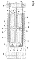
- FIG 3 a section of the device in Figure 2 according to line III-III is shown.
- An epitaxial layer 2 of P type with low dopant concentration is formed on a substrate 1 of P type with high dopant concentration.
- an implant of P type dopant at high concentration for example boron, which is made to diffuse for forming sinker regions 3.
- the deposition of gate oxide 4 the deposition of polysilicon layers 5 over the gate oxide layers 4, and the successive doping of the polysilicon.
- the successive steps of the process for manufacturing the LDMOS device provide the steps for forming the body regions 6 with a P type dopant, which have a central part with high dopant concentration of P type, the implants for forming drain regions 7 and source regions 8 with N type dopant, the formation of intermediate passivant layers 9 over and about the gate oxide layers 4 and the polysilicon layers 5, the deposition of a metal layer for forming metal stripes 10 for contacting the source regions 8, metal stripes 11 and metal stripes 201 for contacting the drain regions 7 and metal stripes 202 for contacting the gate fingers 5.
- Figures 2 and 3 it is shown that for any two polysilicon layers 5 one single contact point Q with the metal stripe 202 is formed and the metal stripes 11 are interdigitated and connected with the metal stripe 201.
- the stripes 10, 11, 201 and 202 are at the same level, therefore the device in Figures 1-3 is a single metallization level device.
- the device according to a first embodiment of the invention provides the presence of blocks 300 of active zones of the device and of inactive zones.
- an epitaxial layer 2 of P type with low dopant concentration is formed on a substrate 1 of P type with high dopant concentration.
- an implant of P type dopant at high concentration for example boron, which is made to diffuse for forming sinker regions 3.
- the successive steps of the process for manufacturing the LDMOS device provide the steps for forming the body regions 6 with a P type dopant, which have a central part with high dopant concentration of P type, the implants for forming drain regions 7 and source regions 8 with N type dopant.
- the process for manufacturing the LDMOS device comprises a step for forming field oxide regions 30, called even LOCOS, over the sinker region 3.
- a first step for depositing field oxide and a second step of thermal diffusion so that said field oxide is diffused inside the body regions 6 occur.
- the formation of intermediate passivant layers 9 over and about the gate oxide layers 4 and the polysilicon layers 5, which are the gates of the elementary cells composing the LDMOS device, and the formation of intermediate passivant layers 91 over the LOCOS regions 30 occur.
- a metal layer for forming the metal stripes 50 adapted for contacting the source regions 8, the metal stripes 11 and metal stripes 110 which are adapted for contacting the drain regions 7 and the metal stripes 60 and 20 occur.
- the metal stripes 50 differently from the metal stripes 10 in Figure 3 are interrupted in the central portion over the LOCOS regions 30 and the intermediate passivant layers 91, along the body stripes 6; in such way the metal stripes 20 may be deposited over the intermediate passivant layers 91 which allow to increase the contact points between the metal bus 60 and the polysilicon layers 5.
- Each separation zone 31 is given therefore by a portion of body region 6 arranged between the source regions 8 placed in the same body region 6.
- the stripes 20 are formed in a transversal direction with respect to the formation of the channel in the elementary cells forming the LDMOS device while the prolongations 21 and 51 are formed in a parallel direction with respect to the formation of the channel in said LDMOS elementary cells. Also the metal stripes 20 are parallel to the metal stripes 11 deriving from the main metal stripe 110.
- the stripes 20, 50, 11, 110 and 60 are at the same level, therefore the device in Figures 4 and 5 is a single metallization level device.
- the resistance R of the gate finger is decreased by means of the presence of the contact points T because two contact points occur for each gate finger; the diminution of the resistance causes a decreasing of the time constant RC and therefore a diminution of the propagation delay of the electric signals.
- FIG. 6 a device according to a second embodiment of the present invention is shown; in the layout it is possible to ascertain that there are three contact points between one gate finger and the metal bus that is necessary to contact it instead of two contact points of the first embodiment. This is due to the formation of a further contact point between the metal stripes 20 and the polysilicon fingers 5, that is a new contact point H placed on the body region 6 which is formed by superimposing further prolongations 22 of the stripes 20 over further prolongations 52 of the polysilicon fingers 5. The contact point H is formed near the central part of the body region 6 and near the central part of the stripes 20 and of the fingers 5. This is obtained by means of a different mask for forming metal stripes 55 adapted for contacting said source regions 3.
- the metal stripes 55 show in a central part a smaller width than the stripes 50 in Figure 4 for the formation of said further contact point H.
- the mask for forming the contacts 81 shows a smaller width in the central part and an interruption in presence of the prolongations 52 of the polysilicon fingers 5.
- the prolongations 52 and 22 have a direction parallel to the formation of the channel of the elementary cells of the LDMOS device.
- the further contact point H allows to furtherly decrease the resistance R that causes a diminution of the time constant RC and therefore a further diminution of the propagation delay of the electric signals.
- the stripes 55, 11, 110, 60 and 20 are at the same level, therefore the device in Figure 6 is a single metallization level device.
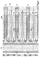
- FIG 7 the layout of the device according to the first or the second embodiment of the present invention is shown.
- the blocks 300 or 301 formed by the elementary cells composing the LDMOS device and by the separation zones 31 are contiguous to each other minimising the Power Recombining effects because any connection does not exist which may form a mismatch between the adjacent blocks 300 or 301.
- the couples of adjacent blocks 300 or 301 are separated from each other by means of a couple of stripes 110 adjacent to each other.
- the couples of metal stripes 110 of each couple of blocks 300 or 301 which as previously said serve for contacting the drain regions of the device, are added to the couple of adjacent stripes 110 or to the single adjacent metal stripe 110 by means of transversal stripes 111 placed on the top of the chip wherein the device is formed as shown in Figure 7.
- the transversal stripes 111 are connected with pads 112 used for outputting or introducing electric signals in the device.
- Each couple of adjacent blocks 300 or 301 shows a metal stripe 60 adapted for contacting the gate fingers of the cells and it is placed between the blocks 300 or 301 forming said couple and in parallel to the stripes 110. Therefore each single metal stripe 60 allows contacting the gate fingers of each elementary cell of the blocks 300 or 301 belonging to the couple. Also, as shown in Figures 4 and 6, each contact point Q allows contacting contemporaneously four polysilicon fingers 5 with the metal stripe 60.
- the couples of metal stripes 60 of each couple of blocks 300 or 301 are added to the adjacent stripes 60 by means of transversal stripes 61 placed on the bottom of the chip wherein the device is formed as shown in Figure 7.
- the transversal stripes 61 are connected with pads 62 used for outputting or introducing electric signals in the device. Therefore the arrangement of the transversal stripes 111 and 61 in the periphery of the chip but in opposite periphery parts of the chip and the consequent arrangement of the pads 112 and 62 in the periphery of the chip and about the series of the blocks 300 or 301, allow to form easily the welding of the wires between the chip and the capacitors of the adaptation network.
Landscapes
- Insulated Gate Type Field-Effect Transistor (AREA)
Abstract
Semiconductor integrated device of metal oxide semiconductor type, comprises first metal stripes, second metal stripes, and third metal stripes where at least one comprises fourth metal stripe(s) placed on separation zone(s). The fourth metal stripe(s) has first prolongation that is placed on second prolongation(s) of material conductor finger(s). Semiconductor integrated device of metal oxide semiconductor (MOS) type, comprises a substrate of a first conductivity type comprising active zones (300) and inactive zones of the semiconductor device; first metal stripes (50) that contact source regions and the active zones; second metal stripes (110, 11) that contact drain regions; and third metal stripes (60) placed on the inactive zones and contact conductor material finger(s) of each elementary cell by forming a contact point (Q) formed by a first prolongation of the finger(s) for connecting with one of the third stripes. The active zones comprise elementary MOS cells of the semiconductor device that are alternated with separation zones. Each one of the elementary MOS cells comprises source region(s), drain region(s), and gate structure(s) comprising first conductor material finger(s) (5). The first metal stripes, second metal stripes and third metal stripes are placed on the substrate of semiconductor material substantially at the same level. At least one of the third metal stripes comprises fourth metal stripe(s) (20) placed on the separation zone(s). The conductor material finger(s) of each elementary cell has second prolongation(s) (51). The fourth metal stripe(s) has first prolongation (21) that is placed on the second prolongation(s) of the material conductor finger(s) to form at least another contact point (T). An independent claim is included for a process for manufacturing an integrated device of the MOS type on a substrate of semiconductor material of a first conductivity type, comprising forming active zones by forming source regions of a second conductivity type inside the substrate, drain regions of the second conductivity type, and gate structures comprising layer(s) of conductor material, the gate structures form with the source regions and drain regions, elementary MOS cells of the device; forming separation zones alternated with the elementary MOS cells; masking and depositing a metal layer on the semiconductor substrate to form first metal stripes for contacting the source regions, second metal stripes for contacting the drain regions and third metal stripes for contacting each conductor material layer of the gate structures at a point (Q); and forming a mask provided with windows on the separation zones and near them for depositing metal to form fourth metal stripes that are placed on the first prolongation of the conductor material to form another contact point (T). The formation of the mask and the deposition of the conductor material of the gate structures allow the formation of first prolongations of the conductor material.
Description
- The present invention refers to a high performance semiconductor integrated device of the MOS type, particularly to a LDMOS device and to the related manufacturing process.
- Actually there is a higher and higher evolution in the field of the radio frequency devices used in communication appliances as, for example, amplifiers in output stages of cellular transmitters. The research of higher and higher performances of said radio frequency devices and of maximum compatibly thereof with the other components of the different radio frequency appliances, it has brought to the use of different technologies for forming these devices as the LDMOS technology.
- The LDMOS semiconductor devices have better features than those of the MOS semiconductor devices at high frequency, that is between 500Mhz and 2Ghz, because they allow a better setting of the input signal and a diminution of the losses of part of the output power for mismatch.
- However a correct design of the input structure and of all the layout of the semiconductor device is necessary to minimize furtherly the mentioned losses. The input structure is mainly constituted by the gate terminal of the LDMOS device.
- In each elementary cell belonging to the LDMOS device the electric connection of the single gate terminals is obtained by means of a single contact point. Therefore, each gate terminal called commonly "gate finger", may be constituted, for a concentrate parameter circuit, by a network RC wherein the resistor R is given by the resistor of the gate finger, formed generally in polysilicon, and the capacity C is essentially given by the capacity between the gate terminal and the source terminal of each single elementary cell. The propagation of a signal through the gate finger may therefore have a delay given by the value of the time constant RC.
- Actually a technology for controlling the resistance of the gate finger consists of placing on the polysilicon of the gate finger a thin layer of high conductivity material as, for example, cobalt or tungsten silicide. Other technologies used provide LDMOS structures having two or three metallization levels in order to define more contact points without decreasing excessively the capacity component.
- Normally the elementary cells belonging to a LDMOS device are placed in separated blocks and at a prefixed distance from each other. This is due to the fact that the arrangement and number thereof can increase the electromagnetic iteration thereof, thus causing a decreasing of the output power. This phenomenon, known even as "Power Combining effect", depends just on the distance between the blocks and on the number of the blocks.
- In view of the state of the art described, it is an object of the present invention to provide a high performance semiconductor integrated device of the MOS type which allows to minimize the aforementioned disadvantages.
- According to present invention, such object is obtained by means of a semiconductor integrated device of the MOS type comprising a substrate of a first conductivity type, said substrate comprising a plurality of active zones and inactive zones of said semiconductor device, said active zones comprising elementary MOS cells of said semiconductor device which are alternated to a plurality of separation zones, each one of said elementary MOS cells comprising at least one source region, at least one drain region and at least one gate structure, said at least one gate structure comprising at least one first conductor material finger, said device comprising first metal stripes adapted for contacting said source regions of the active zones, second metal stripes adapted for contacting the drain regions and third metal stripes placed on the inactive zones and adapted for contacting said at least one conductor material finger of each elementary cell by forming a contact point formed by a first prolongation of said at least one finger for connecting with one of said third stripes, said first metal stripes, said second metal stripes and said third metal stripes being placed on the substrate of semiconductor material substantially at the same level, characterized in that at least one of said third metal stripes comprises at least one fourth metal stripe placed on one of said separation zones, at least one conductor material finger of each elementary cell having at least one second prolongation and said at least one fourth metal stripe having at least one first prolongation adapted for being placed on said at least one second prolongation of said at least one material conductor finger to form at least another contact point.
- Always according to present invention it is possible to provide a process for manufacturing of an integrated device of the MOS type as defined in
claim 21. - Thanks to present invention it is possible to form a semiconductor integrated device of the MOS type which, even if it has only one metallization level, allows to form more contact points for the gate fingers. Also said integrated device has a structure that minimizes the electromagnetic iterations among the blocks of elementary cells of which it is composed.
- The features and the advantages of the present invention will be made evident by the following detailed description of embodiments thereof, shown as not limiting examples in the annexed drawings, wherein:
- Figure 1 is a schematic view of a part of a layout of a LDMOS device according to prior art;
- Figure 2 is a more detailed view of a zone of the layout in Figure 1;
- Figure 3 shows a section of the device in Figure 2 according to line III-III;
- Figure 4 is a schematic view of a part of a layout of a LDMOS device according to a first embodiment of the present invention;
- Figure 5 shows a section of the device in Figure 4 according to line V-V;
- Figure 6 is a schematic view of a part of a layout of a LDMOS device according to a second embodiment of the present invention;
- Figure 7 is a schematic view of a part of the layout of the device according to invention;
-
- In Figure 1 a schematic view of a part of a layout of a LDMOS device according to prior art is shown. The
blocks 100 constituting the active zones of the LDMOS device and which comprise single LDMOS elementary cells (wherein it is meant by elementary cells the structures formed by a source region, a drain region and a gate structure, that is, in such case, a structure composed by means of one thin oxide layer and one polysilicon finger) are separated and are at a prefixed distance from each other for controlling the Power Combining effect and thepads 101 are placed at the middle of the layout among thedifferent blocks 100. For eachblock 100 themetal stripes block 100 and which are placed on inactive zones of said device.
The stripes of eachblock 100 are connected with each other by means of arc-shaped elements 203 or by means ofextensions 205 of thestripes 201 while thestripes 202 are connected with each other by means ofelements 204. - In Figure 2 a zone of a
block 100 of the layout in Figure 1is shown in more detail. The LDMOS device under examination is a device with a single metal layer wherein the polysilicon gate fingers of the single elementary cells forming eachblock 100 are contacted at a single point Q by themetal stripe 202 adapted for connecting said gates to bring the driving signals. - In Figure 3 a section of the device in Figure 2 according to line III-III is shown. An
epitaxial layer 2 of P type with low dopant concentration is formed on asubstrate 1 of P type with high dopant concentration. After a first step of oxidizing and a step of masking followed by a successive etch step for forming windows, it occurs an implant of P type dopant at high concentration, for example boron, which is made to diffuse for formingsinker regions 3. In successive steps it occurs the deposition ofgate oxide 4, the deposition ofpolysilicon layers 5 over thegate oxide layers 4, and the successive doping of the polysilicon. The successive steps of the process for manufacturing the LDMOS device provide the steps for forming thebody regions 6 with a P type dopant, which have a central part with high dopant concentration of P type, the implants for formingdrain regions 7 andsource regions 8 with N type dopant, the formation of intermediate passivant layers 9 over and about thegate oxide layers 4 and thepolysilicon layers 5, the deposition of a metal layer for formingmetal stripes 10 for contacting thesource regions 8,metal stripes 11 andmetal stripes 201 for contacting thedrain regions 7 andmetal stripes 202 for contacting thegate fingers 5. In Figures 2 and 3 it is shown that for any twopolysilicon layers 5 one single contact point Q with themetal stripe 202 is formed and themetal stripes 11 are interdigitated and connected with themetal stripe 201. Thestripes - In Figures 4 and 5 a device according to a first embodiment of the present invention is shown; the elements equal to those of the section in Figure 3 will be represented by the same numeric references. The device according to a first embodiment of the invention provides the presence of
blocks 300 of active zones of the device and of inactive zones. In eachblock 300 anepitaxial layer 2 of P type with low dopant concentration is formed on asubstrate 1 of P type with high dopant concentration. After a first step of oxidizing and a step of masking followed by a successive etch step for forming windows, it occurs an implant of P type dopant at high concentration, for example boron, which is made to diffuse for formingsinker regions 3. In successive steps it occurs the deposition ofgate oxide 4, the deposition of polysilicon layers orfingers 5 over thegate oxide layers 4, and the successive doping of the polysilicon. The successive steps of the process for manufacturing the LDMOS device provide the steps for forming thebody regions 6 with a P type dopant, which have a central part with high dopant concentration of P type, the implants for formingdrain regions 7 andsource regions 8 with N type dopant. - In the layout in figure 4 it is possible to ascertain that three contact points between two gate fingers and the
metal stripe 60 which is necessary to contact them. This is due to the formation ofmetal stripes 20 that derive from amain metal stripe 60, ormetal bus 60, and allow increasing the contact points between themetal bus 60 and the polysilicon layers orfingers 5. Infact prolongations 21 derive from thestripes 20 which are placed overprolongations 51 of eachgate finger 5 to form other contact points T placed on thebody regions 6.Said stripes 20 are formed inseparation zones 31 of theactive zones 300; saidseparation zones 31 are alternated to couples of LDMOS elementary cells in eachblock 300. - In fact the process for manufacturing the LDMOS device comprises a step for forming
field oxide regions 30, called even LOCOS, over thesinker region 3. In such step a first step for depositing field oxide and a second step of thermal diffusion so that said field oxide is diffused inside thebody regions 6 occur. In a successive step the formation of intermediate passivant layers 9 over and about thegate oxide layers 4 and thepolysilicon layers 5, which are the gates of the elementary cells composing the LDMOS device, and the formation of intermediatepassivant layers 91 over theLOCOS regions 30 occur. - In a successive step the deposition of a metal layer for forming the
metal stripes 50 adapted for contacting thesource regions 8, themetal stripes 11 andmetal stripes 110 which are adapted for contacting thedrain regions 7 and themetal stripes metal stripes 50 differently from themetal stripes 10 in Figure 3 are interrupted in the central portion over theLOCOS regions 30 and the intermediatepassivant layers 91, along thebody stripes 6; in such way themetal stripes 20 may be deposited over the intermediatepassivant layers 91 which allow to increase the contact points between themetal bus 60 and thepolysilicon layers 5. Eachseparation zone 31 is given therefore by a portion ofbody region 6 arranged between thesource regions 8 placed in thesame body region 6. Thestripes 20 are formed in a transversal direction with respect to the formation of the channel in the elementary cells forming the LDMOS device while theprolongations metal stripes 20 are parallel to themetal stripes 11 deriving from themain metal stripe 110. Thestripes - The resistance R of the gate finger is decreased by means of the presence of the contact points T because two contact points occur for each gate finger; the diminution of the resistance causes a decreasing of the time constant RC and therefore a diminution of the propagation delay of the electric signals.
- In Figure 6 a device according to a second embodiment of the present invention is shown; in the layout it is possible to ascertain that there are three contact points between one gate finger and the metal bus that is necessary to contact it instead of two contact points of the first embodiment. This is due to the formation of a further contact point between the
metal stripes 20 and thepolysilicon fingers 5, that is a new contact point H placed on thebody region 6 which is formed by superimposingfurther prolongations 22 of thestripes 20 overfurther prolongations 52 of thepolysilicon fingers 5. The contact point H is formed near the central part of thebody region 6 and near the central part of thestripes 20 and of thefingers 5. This is obtained by means of a different mask for formingmetal stripes 55 adapted for contacting saidsource regions 3. In fact themetal stripes 55 show in a central part a smaller width than thestripes 50 in Figure 4 for the formation of said further contact point H. The mask for forming thecontacts 81 shows a smaller width in the central part and an interruption in presence of theprolongations 52 of thepolysilicon fingers 5. Theprolongations stripes - In figure 7 the layout of the device according to the first or the second embodiment of the present invention is shown. The
blocks separation zones 31 are contiguous to each other minimising the Power Recombining effects because any connection does not exist which may form a mismatch between theadjacent blocks adjacent blocks stripes 110 adjacent to each other. The couples ofmetal stripes 110 of each couple ofblocks adjacent stripes 110 or to the singleadjacent metal stripe 110 by means oftransversal stripes 111 placed on the top of the chip wherein the device is formed as shown in Figure 7. Thetransversal stripes 111 are connected withpads 112 used for outputting or introducing electric signals in the device. - Each couple of
adjacent blocks metal stripe 60 adapted for contacting the gate fingers of the cells and it is placed between theblocks stripes 110. Therefore eachsingle metal stripe 60 allows contacting the gate fingers of each elementary cell of theblocks polysilicon fingers 5 with themetal stripe 60. - The couples of
metal stripes 60 of each couple ofblocks adjacent stripes 60 by means oftransversal stripes 61 placed on the bottom of the chip wherein the device is formed as shown in Figure 7. Thetransversal stripes 61 are connected withpads 62 used for outputting or introducing electric signals in the device. Therefore the arrangement of thetransversal stripes pads blocks
Claims (25)
- Semiconductor integrated device of the MOS type comprising a substrate (1, 2) of a first conductivity type, said substrate (1) comprising a plurality of active zones (300; 301) and inactive zones of said semiconductor device, said active zones (300; 301) comprising elementary MOS cells of said semiconductor device which are alternated to a plurality of separation zones (31), each one of said elementary MOS cells comprising at least one source region (8), at least one drain region (7) and at least one gate structure (4, 5), said at least one gate structure (4, 5) comprising at least one first conductor material finger (5), said device comprising first metal stripes (50; 55) adapted for contacting said source regions (8) of the active zones (300; 301), second metal stripes (110, 11) adapted for contacting the drain regions (7) and third metal stripes (60) placed on the inactive zones and adapted for contacting said at least one conductor material finger (5) of each elementary cell by forming a contact point (Q) formed by a first prolongation of said at least one finger (5) for connecting with one of said third stripes (60), said first metal stripes (50; 55), said second metal stripes (110, 11) and said third metal stripes (60) being placed on the substrate (1) of semiconductor material substantially at the same level, characterized in that at least one of said third metal stripes (60) comprises at least one fourth metal stripe (20) placed on one of said separation zones (31), at least one conductor material finger (5) of each elementary cell having at least one second prolongation (51; 52) and said at least one fourth metal stripe (20) having at least one fiverst prolongation (21, 22) adapted for being placed on said at least one second prolongation (51; 52) of said at least one material conductor finger (5) to form at least another contact point (T; H).
- Device according to claim 1, characterized in that each separation zone (31) of said plurality of separation zones is alternated to a couple of elementary MOS cells in each active zone (300; 301).
- Device according to claim 2, characterized in that said second metal stripes (110; 11) comprise at least one further metal stripe (11), said at least one fourth metal stripe (20) being parallel to said at least one further metal stripe (11) and being placed between two of said first stripes (50; 55).
- Device according to claim 3, characterized in that said semiconductor device is a LDMOS device and said elementary MOS cells are LDMOS cells, and in that said substrate (1, 2) comprises an epitaxial layer (2) of the first conductivity type which comprises a plurality of sinker regions (3) of the first type of conductivity and a body regions (6) of the first type of conductivity, each body region (6) being placed on each sinker region (3) and comprises two of said source regions (8) of said elementary LDMOS cells, each one of said plurality of separation zones (31) being constituted by the portion of body region comprises between the source regions (8).
- Device according to claim 4, characterized in that said at least one fourth metal stripe (20) extends in a transversal way with respect to the formation of the channel of each elementary LDMOS cell.
- Device according to claim 5, characterized in that said at least a first prolongation (21; 22) of said at least a fourth stripe (20) and said at least a second prolongation (51; 52) of the conductor material finger (5) extend in a direction parallel to the direction of the channel in each elementary LDMOS cell.
- Device according to claim 4, characterized by comprising a field oxide layer (30) placed in said one separation zone (31), said at least a fourth metal stripes (20) being superimposed on the said field oxide layer (30).
- Device according to claim 7, characterized by comprising a passivant layer (91) placed between said field oxide layer (30) and said at least a fourth metal stripe (20).
- Device according to claim 8, characterized in that said at least one first prolongation (21; 22) of said at least a fourth stripe (20) and said at least a second prolongation (51; 52) of the conductor material finger (5) are placed on body regions (6) of said semiconductor device.
- Device according to claim 9, characterized by comprising a second prolongation (21; 22) of said at least a fourth stripe (20) and a further prolongation (51; 52) of the conductor material finger (5) which are placed together in said active zones (301) of the device.
- Device according to claim 1, characterized in that said conductor material finger (5) is a polysilicon finger.
- Device according to anyone of the preceding claims, characterized in that said at least a fourth metal stripe (20) comprises a plurality of fourth metal stripes (20) placed respectively on each one of said separation zone plurality (31).
- Device according to claim 12, characterized in that each one of said third metal stripes (60) comprises said plurality of fourth metal stripes (20).
- Device according to anyone of the preceding claims, characterized in that the active zones (300; 301) of said plurality of active zones of the device are placed adjacent each other.
- Device according to claim 14, characterized in that said second metal stripes (11, 110) comprise further main metal stripes (110) which are parallel to each others and are placed in a parallel way to the formation of the channel of the elementary MOS cells, said main stripes (110) being placed in inactive zones of the device and each couple of adjacent active zones (300; 301) being comprised between two of said further main metal stripes.
- Device according to claim 15, characterized in that at least one of the further main metal stripes (110) of a couple of active zones (300; 301) is integral with the further metal stripes (110) of the adjacent couple of active zones.
- Device according to claim 16, characterized by comprising first elements (111) for connecting two further main stripes (110) of each couple of active zones (300; 301), said first elements (111) being placed on periphery parts of the chip wherein the device is formed and being associated with first pads (112) for introducing or outputting electric signals.
- Device according to claim 17, characterized in that said third metal stripes (60) are parallel to each others and are parallel to said further metal stripes (110) and in that each couple of adjacent active zones (300; 301) comprises one of said second metal stripes (60) which is placed between said two active zones of the couple.
- Device according to claim 18, characterized by comprising second elements (61) for connecting two third stripes (60) of adjacent couples of active zones (300; 301), said second elements (61) being placed on periphery parts of the chip wherein the device is formed and being associated with second pads (62) for introducing or outputting electric signals.
- Device according to claim 19, characterized in that said first elements (111) and said first pads (112) are placed in the periphery part of the chip which is opposite to the periphery part of the chip wherein said second elements (61) and said second pads (62) are placed.
- Process for manufacturing an integrated device of the MOS type on a substrate (1, 2) of semiconductor material of a first conductivity type, said process comprising steps for the formation of active zones (300; 301) of said device which comprise first sub-steps for forming source regions (8) of a second conductivity type inside said substrate (1, 2), drain regions (7) of the second conductivity type and gate structures (4, 5) comprising at least one layer of conductor material (5), said gate structures (4, 5) forming with the source regions (8) and the drain regions (7) a plurality of elementary MOS cells of said device, said first sub-steps comprising the formation of a plurality of separation zones (31) alternated to said elementary MOS cells, second sub-steps for masking and for depositing a metal layer on said semiconductor substrate in order to form first metal stripes (50; 55) for contacting the source regions, second metal stripes (110, 11) for contacting the drain regions and third metal stripes (60) for contacting each conductor material layer (5) of said gate structures (4, 5) at a point (Q), characterized in that said first sub-steps comprise the formation of a mask and the deposition of said conductor material (5) of the gate structures (4, 5) such as to allow the formation of first prolongations (51; 52) of said conductor material (5) and in that said third sub-steps comprise the formation of a mask provided with windows on said separation zones (31) and near them for depositing metal in order to form fourth metal stripes (20) connected with said third metal stripes (60) and first prolongations (21, 22) of said fourth metal stripes (20) adapted for being placed on said first prolongation (51; 52)of said conductor material (5) in order to form another contact point (T, H).
- Process according to claim 21, characterized in that said first sub-steps comprise the formation of body regions (6) of the first conductivity type in each one of which two source regions (8) of the second conductivity type are formed, each one of said separation zones (31) being constituted by the portion of body region comprised between said two source regions.
- Process according to claim 22, characterized in that said first sub-steps comprise the formation of a field oxide layer (30) on each one of said separation zones (31), each one of said fourth metal stripes (20) being placed on said field oxide layer (30).
- Process according to claim 23, characterized in that said first sub-steps comprise the formation of a passivant layer (91) on each field oxide layer (30), each one of said fourth metal stripes (20) being placed on said passivant layer (91).
- Process according to claim 21, characterized in that said conductor material layers (5) are polysilicon layers.
Priority Applications (3)
| Application Number | Priority Date | Filing Date | Title |
|---|---|---|---|
| EP20020425611 EP1408552A1 (en) | 2002-10-09 | 2002-10-09 | Integrated MOS semiconductor device with high performance and process of manufacturing the same |
| US10/677,108 US6933563B2 (en) | 2002-10-09 | 2003-09-30 | High performance, integrated, MOS-type semiconductor device and related manufacturing process |
| US11/103,772 US7186592B2 (en) | 2002-10-09 | 2005-04-12 | High performance, integrated, MOS-type semiconductor device and related manufacturing process |
Applications Claiming Priority (1)
| Application Number | Priority Date | Filing Date | Title |
|---|---|---|---|
| EP20020425611 EP1408552A1 (en) | 2002-10-09 | 2002-10-09 | Integrated MOS semiconductor device with high performance and process of manufacturing the same |
Publications (1)
| Publication Number | Publication Date |
|---|---|
| EP1408552A1 true EP1408552A1 (en) | 2004-04-14 |
Family
ID=32011070
Family Applications (1)
| Application Number | Title | Priority Date | Filing Date |
|---|---|---|---|
| EP20020425611 Withdrawn EP1408552A1 (en) | 2002-10-09 | 2002-10-09 | Integrated MOS semiconductor device with high performance and process of manufacturing the same |
Country Status (2)
| Country | Link |
|---|---|
| US (2) | US6933563B2 (en) |
| EP (1) | EP1408552A1 (en) |
Families Citing this family (27)
| Publication number | Priority date | Publication date | Assignee | Title |
|---|---|---|---|---|
| US8212317B2 (en) * | 2004-01-29 | 2012-07-03 | Enpirion, Inc. | Integrated circuit with a laterally diffused metal oxide semiconductor device and method of forming the same |
| US8212316B2 (en) * | 2004-01-29 | 2012-07-03 | Enpirion, Inc. | Integrated circuit with a laterally diffused metal oxide semiconductor device and method of forming the same |
| US8253196B2 (en) | 2004-01-29 | 2012-08-28 | Enpirion, Inc. | Integrated circuit with a laterally diffused metal oxide semiconductor device and method of forming the same |
| US8253197B2 (en) * | 2004-01-29 | 2012-08-28 | Enpirion, Inc. | Integrated circuit with a laterally diffused metal oxide semiconductor device and method of forming the same |
| US8212315B2 (en) * | 2004-01-29 | 2012-07-03 | Enpirion, Inc. | Integrated circuit with a laterally diffused metal oxide semiconductor device and method of forming the same |
| US7230302B2 (en) * | 2004-01-29 | 2007-06-12 | Enpirion, Inc. | Laterally diffused metal oxide semiconductor device and method of forming the same |
| US8253195B2 (en) * | 2004-01-29 | 2012-08-28 | Enpirion, Inc. | Integrated circuit with a laterally diffused metal oxide semiconductor device and method of forming the same |
| US7190026B2 (en) * | 2004-08-23 | 2007-03-13 | Enpirion, Inc. | Integrated circuit employable with a power converter |
| US7335948B2 (en) * | 2004-08-23 | 2008-02-26 | Enpirion, Inc. | Integrated circuit incorporating higher voltage devices and low voltage devices therein |
| US7195981B2 (en) * | 2004-08-23 | 2007-03-27 | Enpirion, Inc. | Method of forming an integrated circuit employable with a power converter |
| US7186606B2 (en) * | 2004-08-23 | 2007-03-06 | Enpirion, Inc. | Method of forming an integrated circuit employable with a power converter |
| US7229886B2 (en) * | 2004-08-23 | 2007-06-12 | Enpirion, Inc. | Method of forming an integrated circuit incorporating higher voltage devices and low voltage devices therein |
| US7232733B2 (en) * | 2004-08-23 | 2007-06-19 | Enpirion, Inc. | Method of forming an integrated circuit incorporating higher voltage devices and low voltage devices therein |
| US7214985B2 (en) * | 2004-08-23 | 2007-05-08 | Enpirion, Inc. | Integrated circuit incorporating higher voltage devices and low voltage devices therein |
| US20100009507A1 (en) * | 2008-07-10 | 2010-01-14 | Krutsick Thomas J | Method of constructing cmos device tubs |
| KR101099931B1 (en) * | 2009-10-07 | 2011-12-28 | 전북대학교산학협력단 | LMDMOS transistor |
| CN103578997A (en) * | 2012-07-27 | 2014-02-12 | 北大方正集团有限公司 | Manufacturing method of LDMOS grid electrode and product |
| EP2738809A3 (en) | 2012-11-30 | 2017-05-10 | Enpirion, Inc. | Semiconductor device including gate drivers around a periphery thereof |
| US9418993B2 (en) * | 2013-08-05 | 2016-08-16 | Globalfoundries Inc. | Device and method for a LDMOS design for a FinFET integrated circuit |
| US9673192B1 (en) | 2013-11-27 | 2017-06-06 | Altera Corporation | Semiconductor device including a resistor metallic layer and method of forming the same |
| US10020739B2 (en) | 2014-03-27 | 2018-07-10 | Altera Corporation | Integrated current replicator and method of operating the same |
| US9536938B1 (en) | 2013-11-27 | 2017-01-03 | Altera Corporation | Semiconductor device including a resistor metallic layer and method of forming the same |
| US9508846B2 (en) | 2014-04-18 | 2016-11-29 | Stmicroelectronics S.R.L. | Vertical MOS semiconductor device for high-frequency applications, and related manufacturing process |
| DE102014113465B4 (en) * | 2014-09-18 | 2022-01-13 | Infineon Technologies Austria Ag | electronic component |
| US10103627B2 (en) | 2015-02-26 | 2018-10-16 | Altera Corporation | Packaged integrated circuit including a switch-mode regulator and method of forming the same |
| US10103258B2 (en) * | 2016-12-29 | 2018-10-16 | Texas Instruments Incorporated | Laterally diffused metal oxide semiconductor with gate poly contact within source window |
| US10886399B2 (en) * | 2018-09-07 | 2021-01-05 | Nxp Usa, Inc. | High voltage semiconductor device and method of fabrication |
Citations (7)
| Publication number | Priority date | Publication date | Assignee | Title |
|---|---|---|---|---|
| US5589405A (en) * | 1992-02-18 | 1996-12-31 | Sgs-Thomson Microelectronics, S.R.L. | Method for fabricating VDMOS transistor with improved breakdown characteristics |
| US5744843A (en) * | 1996-08-28 | 1998-04-28 | Texas Instruments Incorporated | CMOS power device and method of construction and layout |
| US5767578A (en) * | 1994-10-12 | 1998-06-16 | Siliconix Incorporated | Surface mount and flip chip technology with diamond film passivation for total integated circuit isolation |
| US5898198A (en) * | 1997-08-04 | 1999-04-27 | Spectrian | RF power device having voltage controlled linearity |
| US5973341A (en) * | 1998-12-14 | 1999-10-26 | Philips Electronics North America Corporation | Lateral thin-film silicon-on-insulator (SOI) JFET device |
| US6020617A (en) * | 1997-05-23 | 2000-02-01 | U.S. Philips Corporation | Lateral MOS transistor with weakly doped drain extension |
| US6084277A (en) * | 1999-02-18 | 2000-07-04 | Power Integrations, Inc. | Lateral power MOSFET with improved gate design |
Family Cites Families (11)
| Publication number | Priority date | Publication date | Assignee | Title |
|---|---|---|---|---|
| US5404040A (en) * | 1990-12-21 | 1995-04-04 | Siliconix Incorporated | Structure and fabrication of power MOSFETs, including termination structures |
| DE69307121T2 (en) * | 1993-02-24 | 1997-04-17 | Sgs Thomson Microelectronics | Completely depleted lateral transistor |
| JP3129223B2 (en) * | 1997-02-28 | 2001-01-29 | 日本電気株式会社 | Semiconductor device |
| US6169309B1 (en) * | 1997-09-30 | 2001-01-02 | Texas Instruments Incorporated | High breakdown-voltage transistor with transient protection |
| US6297533B1 (en) * | 1997-12-04 | 2001-10-02 | The Whitaker Corporation | LDMOS structure with via grounded source |
| US6313512B1 (en) * | 1999-02-25 | 2001-11-06 | Tyco Electronics Logistics Ag | Low source inductance compact FET topology for power amplifiers |
| KR100340925B1 (en) * | 2000-11-04 | 2002-06-20 | 오길록 | Rf power device and method of making the same |
| SE522576C2 (en) * | 2001-03-09 | 2004-02-17 | Ericsson Telefon Ab L M | Radio frequency power LDMOS transistor |
| US6555883B1 (en) * | 2001-10-29 | 2003-04-29 | Power Integrations, Inc. | Lateral power MOSFET for high switching speeds |
| US6677210B1 (en) * | 2002-02-28 | 2004-01-13 | Linear Technology Corporation | High voltage transistors with graded extension |
| US6831332B2 (en) * | 2002-05-25 | 2004-12-14 | Sirenza Microdevices, Inc. | Microwave field effect transistor structure |
-
2002
- 2002-10-09 EP EP20020425611 patent/EP1408552A1/en not_active Withdrawn
-
2003
- 2003-09-30 US US10/677,108 patent/US6933563B2/en not_active Expired - Lifetime
-
2005
- 2005-04-12 US US11/103,772 patent/US7186592B2/en not_active Expired - Lifetime
Patent Citations (7)
| Publication number | Priority date | Publication date | Assignee | Title |
|---|---|---|---|---|
| US5589405A (en) * | 1992-02-18 | 1996-12-31 | Sgs-Thomson Microelectronics, S.R.L. | Method for fabricating VDMOS transistor with improved breakdown characteristics |
| US5767578A (en) * | 1994-10-12 | 1998-06-16 | Siliconix Incorporated | Surface mount and flip chip technology with diamond film passivation for total integated circuit isolation |
| US5744843A (en) * | 1996-08-28 | 1998-04-28 | Texas Instruments Incorporated | CMOS power device and method of construction and layout |
| US6020617A (en) * | 1997-05-23 | 2000-02-01 | U.S. Philips Corporation | Lateral MOS transistor with weakly doped drain extension |
| US5898198A (en) * | 1997-08-04 | 1999-04-27 | Spectrian | RF power device having voltage controlled linearity |
| US5973341A (en) * | 1998-12-14 | 1999-10-26 | Philips Electronics North America Corporation | Lateral thin-film silicon-on-insulator (SOI) JFET device |
| US6084277A (en) * | 1999-02-18 | 2000-07-04 | Power Integrations, Inc. | Lateral power MOSFET with improved gate design |
Also Published As
| Publication number | Publication date |
|---|---|
| US7186592B2 (en) | 2007-03-06 |
| US20040094806A1 (en) | 2004-05-20 |
| US6933563B2 (en) | 2005-08-23 |
| US20050221567A1 (en) | 2005-10-06 |
Similar Documents
| Publication | Publication Date | Title |
|---|---|---|
| US7186592B2 (en) | High performance, integrated, MOS-type semiconductor device and related manufacturing process | |
| US4288800A (en) | Junction field effect transistor | |
| US20020053685A1 (en) | High side and low side guard rings for lowest parasitic performance in an H-bridge configuration | |
| KR20010112238A (en) | Power mos element and method for producing the same | |
| US20020151124A1 (en) | RF power device and method of manufacturing the same | |
| KR20040104731A (en) | Trench dmos transistor structure | |
| KR19990045294A (en) | Field effect transistor and its manufacturing method | |
| US4178605A (en) | Complementary MOS inverter structure | |
| KR100342623B1 (en) | Vertical misfet and method of its production | |
| CN117457741A (en) | A split-gate MOSFET device and its manufacturing method | |
| JPS6042626B2 (en) | Manufacturing method of semiconductor device | |
| US7095080B2 (en) | RF power LDMOS transistor with multiple gate fingers | |
| JPH0834312B2 (en) | Vertical field effect transistor | |
| US6043553A (en) | Multi-emitter bipolar transistor of a self-align type | |
| JP3344381B2 (en) | Semiconductor device and manufacturing method thereof | |
| US6777756B2 (en) | Semiconductor device | |
| WO2003107432A1 (en) | Power semiconductor device and method of manufacturing the same | |
| US6538281B2 (en) | Low on-resistance LDMOS | |
| US12224282B2 (en) | Integrated circuit device including metal-oxide semiconductor transistors | |
| WO2001031711A2 (en) | Vertical insulated gate field-effect device and method of making the same | |
| US6709936B1 (en) | Narrow high performance MOSFET device design | |
| US4498223A (en) | Method of fabrication of monolithic integrated circuit structure | |
| US10217735B2 (en) | Semiconductor switch device | |
| KR20040081048A (en) | Semiconductor device and manufacturing method thereof | |
| US6608349B1 (en) | Narrow/short high performance MOSFET device design |
Legal Events
| Date | Code | Title | Description |
|---|---|---|---|
| PUAI | Public reference made under article 153(3) epc to a published international application that has entered the european phase |
Free format text: ORIGINAL CODE: 0009012 |
|
| AK | Designated contracting states |
Kind code of ref document: A1 Designated state(s): AT BE BG CH CY CZ DE DK EE ES FI FR GB GR IE IT LI LU MC NL PT SE SK TR |
|
| AX | Request for extension of the european patent |
Extension state: AL LT LV MK RO SI |
|
| 17P | Request for examination filed |
Effective date: 20040928 |
|
| AKX | Designation fees paid |
Designated state(s): DE FR GB IT |
|
| STAA | Information on the status of an ep patent application or granted ep patent |
Free format text: STATUS: THE APPLICATION IS DEEMED TO BE WITHDRAWN |
|
| 18D | Application deemed to be withdrawn |
Effective date: 20090505 |