EP1408546A1 - Semiconductor device and production method therefor - Google Patents
Semiconductor device and production method therefor Download PDFInfo
- Publication number
- EP1408546A1 EP1408546A1 EP02743748A EP02743748A EP1408546A1 EP 1408546 A1 EP1408546 A1 EP 1408546A1 EP 02743748 A EP02743748 A EP 02743748A EP 02743748 A EP02743748 A EP 02743748A EP 1408546 A1 EP1408546 A1 EP 1408546A1
- Authority
- EP
- European Patent Office
- Prior art keywords
- insulating film
- substrate
- interlayer insulating
- vacancy
- semiconductor device
- Prior art date
- Legal status (The legal status is an assumption and is not a legal conclusion. Google has not performed a legal analysis and makes no representation as to the accuracy of the status listed.)
- Withdrawn
Links
Images




Classifications
-
- H—ELECTRICITY
- H10—SEMICONDUCTOR DEVICES; ELECTRIC SOLID-STATE DEVICES NOT OTHERWISE PROVIDED FOR
- H10P—GENERIC PROCESSES OR APPARATUS FOR THE MANUFACTURE OR TREATMENT OF DEVICES COVERED BY CLASS H10
- H10P14/00—Formation of materials, e.g. in the shape of layers or pillars
- H10P14/60—Formation of materials, e.g. in the shape of layers or pillars of insulating materials
- H10P14/69—Inorganic materials
- H10P14/692—Inorganic materials composed of oxides, glassy oxides or oxide-based glasses
- H10P14/6938—Inorganic materials composed of oxides, glassy oxides or oxide-based glasses the material containing at least one metal element, e.g. metal oxides, metal oxynitrides or metal oxycarbides
- H10P14/69398—Inorganic materials composed of oxides, glassy oxides or oxide-based glasses the material containing at least one metal element, e.g. metal oxides, metal oxynitrides or metal oxycarbides the material having a perovskite structure, e.g. BaTiO3
-
- H—ELECTRICITY
- H10—SEMICONDUCTOR DEVICES; ELECTRIC SOLID-STATE DEVICES NOT OTHERWISE PROVIDED FOR
- H10P—GENERIC PROCESSES OR APPARATUS FOR THE MANUFACTURE OR TREATMENT OF DEVICES COVERED BY CLASS H10
- H10P14/00—Formation of materials, e.g. in the shape of layers or pillars
- H10P14/40—Formation of materials, e.g. in the shape of layers or pillars of conductive or resistive materials
-
- H—ELECTRICITY
- H10—SEMICONDUCTOR DEVICES; ELECTRIC SOLID-STATE DEVICES NOT OTHERWISE PROVIDED FOR
- H10B—ELECTRONIC MEMORY DEVICES
- H10B53/00—Ferroelectric RAM [FeRAM] devices comprising ferroelectric memory capacitors
-
- H—ELECTRICITY
- H10—SEMICONDUCTOR DEVICES; ELECTRIC SOLID-STATE DEVICES NOT OTHERWISE PROVIDED FOR
- H10B—ELECTRONIC MEMORY DEVICES
- H10B53/00—Ferroelectric RAM [FeRAM] devices comprising ferroelectric memory capacitors
- H10B53/30—Ferroelectric RAM [FeRAM] devices comprising ferroelectric memory capacitors characterised by the memory core region
-
- H—ELECTRICITY
- H10—SEMICONDUCTOR DEVICES; ELECTRIC SOLID-STATE DEVICES NOT OTHERWISE PROVIDED FOR
- H10P—GENERIC PROCESSES OR APPARATUS FOR THE MANUFACTURE OR TREATMENT OF DEVICES COVERED BY CLASS H10
- H10P14/00—Formation of materials, e.g. in the shape of layers or pillars
- H10P14/60—Formation of materials, e.g. in the shape of layers or pillars of insulating materials
- H10P14/65—Formation of materials, e.g. in the shape of layers or pillars of insulating materials characterised by treatments performed before or after the formation of the materials
- H10P14/6516—Formation of materials, e.g. in the shape of layers or pillars of insulating materials characterised by treatments performed before or after the formation of the materials of treatments performed after formation of the materials
- H10P14/6529—Formation of materials, e.g. in the shape of layers or pillars of insulating materials characterised by treatments performed before or after the formation of the materials of treatments performed after formation of the materials by exposure to a gas or vapour
-
- H—ELECTRICITY
- H10—SEMICONDUCTOR DEVICES; ELECTRIC SOLID-STATE DEVICES NOT OTHERWISE PROVIDED FOR
- H10W—GENERIC PACKAGES, INTERCONNECTIONS, CONNECTORS OR OTHER CONSTRUCTIONAL DETAILS OF DEVICES COVERED BY CLASS H10
- H10W20/00—Interconnections in chips, wafers or substrates
- H10W20/01—Manufacture or treatment
- H10W20/071—Manufacture or treatment of dielectric parts thereof
- H10W20/072—Manufacture or treatment of dielectric parts thereof of dielectric parts comprising air gaps
-
- H—ELECTRICITY
- H10—SEMICONDUCTOR DEVICES; ELECTRIC SOLID-STATE DEVICES NOT OTHERWISE PROVIDED FOR
- H10W—GENERIC PACKAGES, INTERCONNECTIONS, CONNECTORS OR OTHER CONSTRUCTIONAL DETAILS OF DEVICES COVERED BY CLASS H10
- H10W20/00—Interconnections in chips, wafers or substrates
- H10W20/40—Interconnections external to wafers or substrates, e.g. back-end-of-line [BEOL] metallisations or vias connecting to gate electrodes
- H10W20/45—Interconnections external to wafers or substrates, e.g. back-end-of-line [BEOL] metallisations or vias connecting to gate electrodes characterised by their insulating parts
- H10W20/46—Interconnections external to wafers or substrates, e.g. back-end-of-line [BEOL] metallisations or vias connecting to gate electrodes characterised by their insulating parts comprising air gaps
-
- H—ELECTRICITY
- H10—SEMICONDUCTOR DEVICES; ELECTRIC SOLID-STATE DEVICES NOT OTHERWISE PROVIDED FOR
- H10W—GENERIC PACKAGES, INTERCONNECTIONS, CONNECTORS OR OTHER CONSTRUCTIONAL DETAILS OF DEVICES COVERED BY CLASS H10
- H10W20/00—Interconnections in chips, wafers or substrates
- H10W20/40—Interconnections external to wafers or substrates, e.g. back-end-of-line [BEOL] metallisations or vias connecting to gate electrodes
- H10W20/45—Interconnections external to wafers or substrates, e.g. back-end-of-line [BEOL] metallisations or vias connecting to gate electrodes characterised by their insulating parts
- H10W20/47—Interconnections external to wafers or substrates, e.g. back-end-of-line [BEOL] metallisations or vias connecting to gate electrodes characterised by their insulating parts comprising two or more dielectric layers having different properties, e.g. different dielectric constants
-
- H—ELECTRICITY
- H10—SEMICONDUCTOR DEVICES; ELECTRIC SOLID-STATE DEVICES NOT OTHERWISE PROVIDED FOR
- H10W—GENERIC PACKAGES, INTERCONNECTIONS, CONNECTORS OR OTHER CONSTRUCTIONAL DETAILS OF DEVICES COVERED BY CLASS H10
- H10W20/00—Interconnections in chips, wafers or substrates
- H10W20/40—Interconnections external to wafers or substrates, e.g. back-end-of-line [BEOL] metallisations or vias connecting to gate electrodes
- H10W20/45—Interconnections external to wafers or substrates, e.g. back-end-of-line [BEOL] metallisations or vias connecting to gate electrodes characterised by their insulating parts
- H10W20/48—Insulating materials thereof
-
- H—ELECTRICITY
- H10—SEMICONDUCTOR DEVICES; ELECTRIC SOLID-STATE DEVICES NOT OTHERWISE PROVIDED FOR
- H10P—GENERIC PROCESSES OR APPARATUS FOR THE MANUFACTURE OR TREATMENT OF DEVICES COVERED BY CLASS H10
- H10P14/00—Formation of materials, e.g. in the shape of layers or pillars
- H10P14/60—Formation of materials, e.g. in the shape of layers or pillars of insulating materials
- H10P14/63—Formation of materials, e.g. in the shape of layers or pillars of insulating materials characterised by the formation processes
- H10P14/6326—Deposition processes
- H10P14/6342—Liquid deposition, e.g. spin-coating, sol-gel techniques or spray coating
-
- H—ELECTRICITY
- H10—SEMICONDUCTOR DEVICES; ELECTRIC SOLID-STATE DEVICES NOT OTHERWISE PROVIDED FOR
- H10P—GENERIC PROCESSES OR APPARATUS FOR THE MANUFACTURE OR TREATMENT OF DEVICES COVERED BY CLASS H10
- H10P14/00—Formation of materials, e.g. in the shape of layers or pillars
- H10P14/60—Formation of materials, e.g. in the shape of layers or pillars of insulating materials
- H10P14/66—Formation of materials, e.g. in the shape of layers or pillars of insulating materials characterised by the type of materials
- H10P14/665—Porous materials
-
- H—ELECTRICITY
- H10—SEMICONDUCTOR DEVICES; ELECTRIC SOLID-STATE DEVICES NOT OTHERWISE PROVIDED FOR
- H10P—GENERIC PROCESSES OR APPARATUS FOR THE MANUFACTURE OR TREATMENT OF DEVICES COVERED BY CLASS H10
- H10P14/00—Formation of materials, e.g. in the shape of layers or pillars
- H10P14/60—Formation of materials, e.g. in the shape of layers or pillars of insulating materials
- H10P14/66—Formation of materials, e.g. in the shape of layers or pillars of insulating materials characterised by the type of materials
- H10P14/668—Formation of materials, e.g. in the shape of layers or pillars of insulating materials characterised by the type of materials the materials being characterised by the deposition precursor materials
- H10P14/6681—Formation of materials, e.g. in the shape of layers or pillars of insulating materials characterised by the type of materials the materials being characterised by the deposition precursor materials the precursor containing a compound comprising Si
- H10P14/6684—Formation of materials, e.g. in the shape of layers or pillars of insulating materials characterised by the type of materials the materials being characterised by the deposition precursor materials the precursor containing a compound comprising Si the compound comprising silicon and oxygen
- H10P14/6686—Formation of materials, e.g. in the shape of layers or pillars of insulating materials characterised by the type of materials the materials being characterised by the deposition precursor materials the precursor containing a compound comprising Si the compound comprising silicon and oxygen the compound being a molecule comprising at least one silicon-oxygen bond and the compound having hydrogen or an organic group attached to the silicon or oxygen, e.g. a siloxane
-
- H—ELECTRICITY
- H10—SEMICONDUCTOR DEVICES; ELECTRIC SOLID-STATE DEVICES NOT OTHERWISE PROVIDED FOR
- H10P—GENERIC PROCESSES OR APPARATUS FOR THE MANUFACTURE OR TREATMENT OF DEVICES COVERED BY CLASS H10
- H10P14/00—Formation of materials, e.g. in the shape of layers or pillars
- H10P14/60—Formation of materials, e.g. in the shape of layers or pillars of insulating materials
- H10P14/69—Inorganic materials
- H10P14/692—Inorganic materials composed of oxides, glassy oxides or oxide-based glasses
- H10P14/6921—Inorganic materials composed of oxides, glassy oxides or oxide-based glasses containing silicon
- H10P14/6922—Inorganic materials composed of oxides, glassy oxides or oxide-based glasses containing silicon the material containing Si, O and at least one of H, N, C, F or other non-metal elements, e.g. SiOC, SiOC:H or SiONC
Definitions
- the present invention relates to a semiconductor device and a method of manufacturing the semiconductor device, and more particularly to an inorganic dielectric film having a low dielectric constant.
- the fluorine can be added in an element ratio of approximately several % at most because the heat resistance of the insulating film is deteriorated. For this reason, there is a problem in that a specific dielectric constant can be reduced by only 10% to 15% as compared with a conventional silica based interlayer insulating film.
- the porous structure is not closed. If the porous structure is not closed, the moisture resistance of the interlayer insulating film is remarkably reduced so that the reliability of the semiconductor device is deteriorated.
- the invention has been made in consideration of the actual circumstances and has an object to provide an insulating film having a low dielectric constant and a great mechanical strength.
- the invention has an object to provide a semiconductor device capable of reducing both a capacity between wiring layers and a capacity between wirings in microfabrication and an increase in integration in the semiconductor device.
- the invention provides a semiconductor device comprising an inorganic insulating film formed on a surface of a substrate and having a periodic porous structure which includes vacancies having two kinds of different sizes or more, at least the vacancy having a first size being arranged periodically.
- the inorganic insulating film should include the vacancies having first and second sizes, the vacancy having the second size being arranged randomly.
- the inorganic insulating film should have a composite periodic porous structure which includes the vacancies having first and second sizes, both of the vacancies having the first and second sizes being arranged periodically.
- the vacancies in various sizes to have the periodic porous structure in which at least the vacancy having the first size is arranged periodically. Consequently, more vacancies can be included.
- the dielectric constant of air is low. Therefore, the dielectric constant can be reduced considerably and the dielectric constant of the insulating film can be reduced extremely.
- the inorganic insulating film should be obtained by repetitively arranging a first porous structure domain comprising a skeletal structure in which a cylindrical vacancy is arranged periodically and a large number of small holes are included and a second porous structure domain comprising a skeletal structure in which a layered vacancy is arranged periodically in a perpendicular direction to the surface of the substrate and a large number of small holes are included.
- the skeletal structure having the small holes is employed, more vacancies can be included and the dielectric constant can further be reduced.
- the vacancy can have such a closed structure as to have no opening portion for an upper wiring and a lower wiring in the case in which the inorganic insulating film is particularly used as an interlayer insulating film.
- the inorganic insulating film can serve as a thin film having a low dielectric constant which is excellent in a moisture resistance, has a high reliability and is effective. Moreover, it is possible to obtain a uniform electrical characteristic.
- the porous structure is oriented in a direction which is varied for each domain. Consequently, the opening portions of the vacancies can be closed each other.
- a thin film which has a great moisture resistance to be almost equivalent to the moisture resistance of a minute film, is also excellent in a mechanical strength because of the periodic structure and has an ultimately low dielectric constant.
- a space between layers is supported on the adjacent layers. Consequently, the layered periodic porous shape to be usually supposed to be unstable can be constructed stably with a great mechanical strength.
- the inorganic insulating film should be obtained by repetitively laminating, in parallel with the surface of the substrate, a first porous structure domain layer comprising a skeletal structure in which a cylindrical vacancy is arranged periodically and a large number of small holes are included and a second porous structure domain layer in which a layered vacancy is arranged periodically in parallel with the surface of the substrate and a large number of small holes are included.
- the vacancy can have such a closed structure as to have no opening portion with respect to the upper wiring and the lower wiring.
- the inorganic insulating film can serve as a thin film having a low dielectric constant which is excellent in a moisture resistance, has a very high reliability and is effective.
- the inorganic insulating film should be an interlayer insulating film provided between a semiconductor substrate or a first layer wiring conductor formed on the semiconductor substrate and a second layer wiring conductor.
- the insulating film having a low capacity can be formed. Therefore, a parasitic capacitance can be reduced and the speed of a semiconductor device can be increased.
- the interlayer insulating film should include a first interlayer insulating film region which is formed on the first layer wiring conductor and has a contact hole to come in contact with the first layer wiring conductor and a second interlayer insulating film to be filled in a wiring region of the second layer wiring conductor formed on the first interlayer insulating film, the first interlayer insulating film being constituted by a second porous structure domain having a skeletal structure in which a layered vacancy is arranged periodically and a large number of small holes are included.
- the second porous structure domain having the skeletal structure in which the layered vacancy is arranged periodically in a region surrounding the contact hole and a large number of small holes are provided. Consequently, it is possible to further reduce the capacity between the layers.
- the interlayer insulating film should include a first interlayer insulating film formed on the first layer wiring conductor and having a contact hole to come in contact with the first layer wiring conductor, and a second interlayer insulating film to be filled in a wiring region of the second layer wiring conductor formed on the first interlayer insulating film, the first interlayer insulating film being constituted by a second porous structure domain having a skeletal structure in which a layered vacancy is arranged periodically and a large number of small holes are included and the second interlayer insulating film being constituted by a first porous structure domain having a skeletal structure in which a cylindrical vacancy is arranged periodically and a large number of small holes are included.
- the second porous structure domain having the skeletal structure in which the layered vacancy is arranged periodically in the region surrounding the contact hole and a large number of small holes are provided. Consequently, the capacity between the layers can be reduced considerably.
- the cylindrical vacancy is arranged in a line direction in an upper layer wiring region constituting an insulating film between lines. Therefore, a capacity in the line direction can be reduced more considerably.
- the interlayer insulating film should include a first interlayer insulating film formed on the first layer wiring conductor and having a contact hole to come in contact with the first layer wiring conductor, and a second interlayer insulating film to be filled in a wiring region of the second layer wiring conductor formed on the first interlayer insulating film, the first interlayer insulating film being constituted by a second porous structure domain having a skeletal structure in which a layered vacancy formed in parallel with the surface of the substrate is arranged periodically and a large number of small holes are included and the second interlayer insulating film being constituted by a third porous structure domain having a skeletal structure in which a layered vacancy formed almost perpendicularly to the surface of the substrate is arranged periodically and a large number of small holes are included.
- the second porous structure domain having the skeletal structure in which the layered vacancy is arranged periodically in the region surrounding the contact hole in parallel with the surface of the substrate and a large number of small holes are included. Consequently, the capacity between the layers can be reduced considerably.
- the layered vacancy is arranged periodically almost perpendicularly to the surface of the substrate in an upper layer wiring region constituting the insulating film between lines. Therefore, a capacity in the line direction can be reduced still more. Moreover, it is possible to provide a semiconductor device having a high reliability without a problem of a short circuit between wirings.
- the step of manufacturing an interlayer insulating film comprises the step of generating a precursor solution to contain a silica derivative including a siloxane skeleton having a six-membered ring or more and a surfactant and to have such a composition ratio that a vacancy is arranged periodically, the precrosslinking step of raising a temperature of the precursor solution to start a crosslinking reaction, the contact step of causing the precursor solution starting to be crosslinked at the precrosslinking step to come in contact with a surface of a substrate, and the step of burning the substrate with which the precursor solution is caused to come in contact and decomposing and removing the surfactant, thereby forming an insulating film.
- the silica derivative including a siloxane skeleton having a six-membered ring or more is used. Therefore, the skeletal structure itself is formed to have small holes. Thus, it is possible to further reduce the dielectric constant while maintaining the mechanical strength.
- the step of manufacturing an interlayer insulating film comprises the step of generating a precursor solution to contain a silica derivative including a siloxane skeleton having a six-membered ring or more and a surfactant and to have such a composition ratio that a vacancy is arranged periodically, the contact step of causing the precursor solution to come in contact with a surface of a substrate, the precrosslinking step of raising a temperature of the precursor solution to start a crosslinking reaction, and the step of burning the substrate and decomposing and removing the surfactant, thereby forming an insulating film.
- the silica derivative including a siloxane skeleton having a six-membered ring or more is used. Therefore, the skeletal structure itself is formed to have small holes. Thus, it is possible to further reduce the dielectric constant while maintaining the mechanical strength.
- the invention provides a method comprising the step of generating a first precursor solution to contain a silica derivative including a siloxane skeleton having a six-membered ring or more and a surfactant and to have such a first composition ratio that a vacancy is arranged periodically, the step of generating a second precursor solution to contain a silica derivative including a siloxane skeleton having a six-membered ring or more and a surfactant and to have such a second composition ratio that a vacancy is arranged periodically, the precrosslinking step of raising temperatures of the first and second precursor solutions to start a crosslinking reaction, the contact step of causing the firstandsecondprecursorsolutions starting to be crosslinked at the precrosslinking step to come in contact with a surface of a substrate, and the step of burning the substrate with which the first and second precursor solutions are caused to come in contact and decomposing and removing the surfactant, thereby forming an insulating film.
- the interlayer insulating film having two kinds of different periodic structures or more, for example, the interlayer insulating film obtained by repetitively laminating, in parallel with the surface of the substrate, the first porous structure domain layer having the cylindrical vacancy arranged periodically and the second porous structure domain layer having the layered vacancy arranged periodically in parallel with the surface of the substrate.
- the formation can be carried out at a low temperature. Also in case of use for the interlayer insulating film of an integrated circuit, therefore, it is possible to form an insulating film having a high reliability without influencing a substrate.
- the insulating film can be formed without executing the heating step at 500°C or more. Also in the case in which an aluminum wiring is to be used, therefore, the invention can be applied.
- the insulating film can be formed by the contact of a liquid. Consequently, it is also possible to form a pattern with high precision in a minute region. Thus, the reliability can be enhanced.
- the method according to the invention is characterized in that the first and second precursor solutions are caused to come in contact with the surface of the substrate and the precrosslinking reaction is then started.
- the inorganic insulating film in which the vacancy is formed with two kinds of periodicities or more easily and efficiently.
- the substrate should be repetitively immersed sequentially in the first and second precursor solutions at the contact step.
- the contact step should include the step of immersing the substrate in the first precursor solution and pulling up the substrate at a desirable speed and the step of immersing the substrate in the second precursor solution and pulling up the substrate at a desirable speed.
- first and second precursor solutions should be repetitively applied sequentially onto the substrate at the contact step.
- the contact step should be the spin coating step of dropping the first and second precursor solutions onto the substrate and rotating the substrate.
- the thickness of a film and a vacancy rate can easily be regulated and the insulating film having a low dielectric constant can be formed with a high productivity.
- 1S denotes a silicon substrate
- 12 denotes a first wiring layer
- 13a denotes a first interlayer insulating film
- 13b denotes a second interlayer insulating film
- 13S denotes a second interlayer insulating film
- 14 denotes a second wiring layer
- H denotes a contact hole
- h denotes a small hole
- 1 denotes a silicon substrate
- 2 denotes an isolating film
- 3 denotes a gate insulating film
- 4 denotes a gate electrode
- 5 denotes a source region
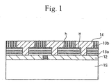
- 6 denotes a drain region
- 7 denotes an insulating film
- 8 denotes a contact hole
- 9 denotes a lower electrode
- 10 denotes a ferroelectric film
- 11 denotes an upper electrode.
- a semiconductor device having a multilayer wiring structure using, as an interlayer insulating film, a thin film having a low dielectric constant which comprises a skeletal structure including a large number of small holes.
- the semiconductor device is characterized in that an interlayer insulating film is constituted by an insulating film having a low dielectric constant in a two-layer structure, a first interlayer insulating film 13a having a contact hole H to come in contact with a first wiring layer 12 is constituted by a second porous structure domain having a skeletal structure in which a layered vacancy is arranged periodically in parallel with the surface of a substrate and a large number of small holes are included, and a second interlayer insulating film 13b to be filled in the wiring region of a second wiring layer 14 on the upper layer side which is formed on the first interlayer insulating film 13a is constituted by a first porous structure domain having a skeletal structure in which a cylindrical vacancy is arranged periodically and a large number of small holes are included.
- the lower layer side of the interlayer insulating film to be formedbetween the first wiring layer 12 and the second wiring layer 14 which are provided on the surface of an element region surrounded by an isolating film (not shown) formed on the surface of a silicon substrate 1S is set to be the first interlayer insulating film 13a having a skeletal structure in which a layered vacancy is arranged periodically in parallel with the surface of the substrate and a large number of small holes h are included
- the second interlayer insulating film 13b to be formed as a line insulating film in the wiring pattern region of the second wiring layer on the upper layer side is constituted by the first porous structure domain having a skeletal structure in which a cylindrical vacancy is arranged periodically and a large number of small holes are included.
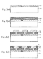
- a desirable semiconductor region is formed on the surface of a silicon substrate 1s and a first wiring layer is thus formed by an ordinary method.
- a thin mesoporous silica film comprising a second periodic porous structure domain in which a layered vacancy is arranged periodically in parallel with the surface of the substrate is formed in parallel with the surface of the substrate by the method according to the invention (Fig. 2(b)).
- cation type cetyltrimethyl ammonium bromide C 16 H 33 N + (CH 3 ) 3 Br -
- CTAB cetyltrimethyl ammonium bromide
- HSQ Hydrogen silosesquioxane
- HCl hydrochloric acid
- the silica derivative is polymerized by a hydrolytic polycondensation reaction (the precrosslinking step) so that the periodic autoaggregate of the surfactant is formed.
- the autoaggregate forms a spherical micelle structure (Fig. 4(b)) obtained by agglutinating a plurality of molecules with C 16 H 33 N + (CH 3 ) 3 Br - to be one molecule as shown in Fig. 4(a).
- a spherical micelle structure FIG. 4(b)
- a layer structure FIG. 4(d) having a vacancy oriented is formed.
- the substrate is pulled up and is washed and dried, and is then heated and burned for 3 hours in a nitrogen atmosphere at 400°C to thermally decompose and remove the surfactant in a template completely, thereby forming a pure and thin mesoporous silica film.
- the first interlayer insulating film 13a having a layered vacancy arranged in parallel with the surface of the substrate is formed.
- Fig. 4(f) is an enlarged explanatory view. An autoaggregate having a high concentration shown in Fig. 4(d) is formed and is burned. Consequently, it is possible to form an inorganic insulating film which has a skeletal structure including a large number of small holes and is provided with the layered vacancy.
- a through hole H is formed on the first interlayer insulating film 13a and the second wiring layer 14 is formed by the ordinary method.
- the second interlayer insulating film 13b is formed.
- the formation is carried out in the same manner as in the step of forming the first interlayer insulating film 13a, and only the composition of the precursor solution is changed. Referring to the molar ratio of preparation of the precursor solution, 0.05 of the surfactant, 0.1 of the silica derivative and 2 of the acid catalyst for 100 of the solvent are mixed. The formation is carried out at just the same other steps.
- the second interlayer insulating film 13b having a skeletal structure in which a cylindrical vacancy is formed periodically and a large number of small holes are included.
- the concentration of the spherical micelle structure obtained by agglutinating a plurality of molecules with C 16 H 33 N + (CH 3 ) 3 Br - to be one molecule is further increased.
- a cylindrical member having the vacancy arranged is formed and an autoaggregate shown in Fig. 4(c) is formed and burned. Consequently, there is obtained the second interlayer insulating film 13b having the first porous structure domain in which a cylindrical vacancy is arranged periodically as shown in an enlarged explanatory view of Fig. 4(e).
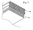
- Fig. 5 is an explanatory view showing the structure of a section in this state.
- the interlayer insulating film is constituted by the first interlayer insulating film 13a formed by a porous thin filmhaving a skeletal structure inwhich the vacancy is formed like a layer and a large number of small holes are included and the second interlayer insulating film 13b having a skeletal structure in which the cylindrical vacancy is arranged periodically and a large number of small holes are included.
- the interlayer insulating film constitutes the second porous structure domain in which the layered vacancy is arranged periodically in the region surrounding the contact hole H. Consequently, a capacity between the layers can be reduced.
- the layered vacancy is arranged in parallel with the wirings. Consequently, a capacity in a wiring direction can be reduced.
- the direction of the array of the cylindrical vacancy is oriented in parallel with the wiring direction of the wiring pattern of the second wiring layer 14. Therefore, it is possible to provide a semiconductor device having a high reliability without a problem of a short circuit between wirings.
- the interlayer insulating film is constituted by the insulating film having a low dielectric constant in the two-layer structure
- the lower layer side is constituted by the second porous structure domain having the layered vacancy arranged periodically in parallel with the surface of the substrate
- the upper layer side is constituted by the first porous structure domain having the cylindrical vacancy arranged periodically in the first embodiment
- the upper layer side may be constitutedby a third porous structure domain to be provided perpendicularly to the surface of the substrate in parallel with a main wiring in place of the cylindrical vacancy.
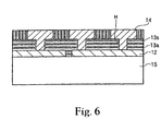
- Fig. 6 shows the structure. More specifically, as shown in Fig. 6, the semiconductor device is characterized in that an interlayer insulating film is constituted by an insulating film having a low dielectric constant in a two-layered structure, a first interlayer insulating film 13a having a contact hole H to come in contact with a first wiring layer 12 is constituted by a second porous structure domain having a skeletal structure in which a layered vacancy is arranged periodically in parallel with the surface of a substrate and a large number of small holes are included, and a second interlayer insulating film 13S to be filled in the wiring region of a second wiring layer 14 on the upper layer side which is formed on the first interlayer insulating film 13a is constituted by the third porous structure domain in which a layered vacancy to be almost perpendicular to the surface of the substrate is arranged periodically.
- an interlayer insulating film is constituted by an insulating film having a low dielectric constant in a two-layered structure
- the lower layer side of the interlayer insulating film to be formedbetween the first wiring layer 12 and the second wiring layer 14 which are provided on the surface of an element region surrounded by an isolating film (not shown) formed on the surface of a silicon substrate 1s is set to be the first interlayer insulating film 13a in which a layered vacancy is arranged periodically in parallel with the surface of the substrate, and the second interlayer insulating film 13S to be formed as a line insulating film in the wiring pattern region of the second wiring layer on the upper layer side is constituted by the third porous structure domain to be provided perpendicularly to the surface of the substrate in parallel with the main wiring.
- the wiring is provided in parallel with the main wiring. Consequently, a multilayered insulating wall is present between the wirings and a short circuit between the wirings can also be prevented better.
- the FRAM comprises a switching transistor formed in an element region surrounded by an isolating film 2 formed on the surface of a silicon substrate 1 and a ferroelectric capacitor and is characterized in that a thin film 7 having a low dielectric constant according to the invention is used as an interlayer insulating film between the switching transistor and a lower electrode 9 of the ferroelectric capacitor in the invention.
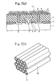
- the thin film having a low dielectric constant is characterized by a first porous structure domain 7c having a skeletal structure in which a cylindrical vacancy is arranged periodically and a large number of small holes h are included as shown in an enlarged perspective view illustrating a main part in Fig. 7(b).
- the vacancy can have such a closed structure as to have no opening portion with respect to an upper layer wiring and a lower layer wiring. Consequently, it is possible to produce the advantages of a thin film having a low dielectric constant which is excellent in a moisture resistance, has a very high reliability and is effective.
- the switching transistor comprises a gate electrode formed on the surface of the silicon substrate 1 through a gate insulating film 3, and a source region 5 and a drain region 6 which are formed to interpose the gate electrode therebetween, and the lower electrode 9 is connected to the drain region 6 through a contact 8, while a source - drain region is connected to a bit line BL.
- a ferroelectric capacitor is constituted by interposing a ferroelectric thin film 10 comprising PZT between the lower electrode 9 and an upper electrode 11.
- a gate electrode 4 is formed on the surface of the silicon substrate 1 through the gate insulating film 3 and an impurity is diffused by using the gate electrode 4 as a mask, thereby forming the source region 5 and the drain region 6 (Fig. 8(a)).
- a thin mesoporous silica film is formed to include a plurality of periodic porous structure domains having a cylindrical vacancy oriented in one direction in parallel with the surface of the substrate (Fig. 8(b)).
- cation type cetyltrimethyl ammonium bromide C 16 H 33 N + (CH 3 ) 3 Br -
- MSQ Methyl silsesquioxane
- HCl hydrochloric acid
- the first precursor solution mixing 0.05 of the surfactant, 0.1 of the silica derivative and 2 of the acid catalyst for 100 of the solvent and a second precursor solution mixing 0.5 of the surfactant, 5 of the silica derivative and 2 of the acid catalyst for 100 of the solvent.
- the first and second precursor solutions thus formed are dropped from respective nozzles onto the surface of the substrate 1 mounted on a spinner and a rotation is carried out at 500 to 5000 rpm so that a thin mesoporous silica film is obtained.
- the silica derivative is held at 30°C to 150°C for 1 to 120 hours and is thereby polymerized by a hydrolytic polycondensation reaction (the precrosslinking step), resulting in the formation of a thin mesoporous silica film having the periodic autoaggregate of the surfactant to be a template.
- the precrosslinking step is desirably carried out at 60°C to 120°C, and more desirably, at 70°C to 90°C for approximately 12 to 72 hours.
- the thin film 7 having a low dielectric constant according to the embodiment of the invention is thus formed, it is to be actually formed in two stages in order to provide the bit line BL. It is also possible to form an interlayer insulating film in a two-layer structure having different vacancy arrays by using precursor solutions having different composition ratios before and after the formation of the bit line BL.
- the precursor solution is applied onto the surface of the substrate and the precrosslinking is then carried out in the embodiment, it is also possible to carry out the precrosslinking and to then apply the precursor solution onto the surface of the substrate.
- the precursor solutions are mixed with difficulty and mutual states can be maintained. Consequently, an interlayer insulating film having a plurality of periodic porous structures can be formed more easily.
- a contact hole 8 is formed on the thin film 7 having a low dielectric constant by an ordinary method. Thereafter, a buried plug comprising a doped polycrystalline silicon layer in a high concentration is formed in the contact hole. Subsequently, iridium is set to be a target and an iridium oxide layer is formed by using a mixed gas of argon and oxygen. Furthermore, a platinum layer is formed on the iridium oxide layer by using platinum as a target. As shown in Fig. 8(c), thus, the iridium oxide layer having a thickness of approximately 50 nm and the platinum layer having a thickness of approximately 200 nm are formed and are patterned by photolithography. Thus, the lower electrode 9 is formed.
- a PZT film is formed as the ferroelectric film 10 on the lower electrode 9 by a sol-gel method.
- a mixed solution of Pb(CH 3 COO) 2 ⁇ 3H 2 O, Zr(t-OC 4 H 9 ) 4 and Ti(i-OC 3 H 7 ) 4 was used as a starting material.
- the mixed solution was subjected to spin coating and was then dried at 150°C, and was temporarily burned for 30 minutes at 400°C in a dry air atmosphere. This operation was repeated five times and a heat treatment was carried out at 700°C or more in an O 2 atmosphere.
- the ferroelectric film 10 having a thickness of 250 nm was formed.
- PbZr x Ti 1-x O 3 x is set to be 0.52 (which will be hereinafter referred to as PZT (52/48)) and a PZT film is thus formed (Fig. 8(d)).
- a laminated film 11 of iridium oxide and iridium is formed on the ferroelectric film 10 by sputtering.
- the laminated film comprising the iridium oxide layer and the iridium layer is set to be the upper electrode 11.
- the iridium layer and the iridium oxide layer are formed to have a thickness of 200 nm in total.
- a ferroelectric capacitor can be obtained and the FRAM shown in Fig. 7 can be formed.
- the interlayer insulating film is constituted by the thin film having a low dielectric constant which is formed by a thin mesoporous silica film. Therefore, the capacity of the interlayer insulating film can be reduced. Thus, it is possible to form an FRAM having an excellent switching characteristic and capable of carrying out a high-speed operation.
- the periodic porous structure is used. Therefore, a mechanical strength can be increased.
- the interlayer insulating film is constituted by the first porous structure domain having the skeletal structure in which the cylindrical vacancy is arranged periodically and a large number of small holes are included. Consequently, it is possible to form an insulating film having a low dielectric constant in which a mechanical strength is great.
- the operating speed of a device can be increased. Accordingly, theinterlayerinsulating film can have a long lifetime.
- the composition of the first precursor solution is not restricted to the composition according to the embodiment but it is desirable that 0.01 to 0.1 of the surfactant, 0.01 to 0.5 of the silica derivative and 0 to 5 of the acid catalyst for 100 of the solvent should be used.
- the precursor solution having such a structure it is possible to form an insulating film having a low dielectric constant which includes a cylindrical vacancy.
- the composition of the second precursor solution is not restricted to the composition according to the embodiment but it is desirable that 0.1 to 10 of the surfactant, 0.5 to 10 of the silica derivative and 0 to 5 of the acid catalyst for 100 of the solvent should be used.
- the precursor solution having such a structure it is possible to form an insulating film having a low dielectric constant which includes a layered vacancy.
- C 16 H 33 N + (CH 3 ) 3 Br - cation type cetyltrimethyl ammonium bromide
- C 16 H 33 N + (CH 3 ) 3 Br - cation type cetyltrimethyl ammonium bromide
- an alkali ion such as an Na ion is used as the catalyst, a semiconductor material is deteriorated. For this reason, it is desirable that a cation type surfactant should be used and an acid catalyst should be used for the catalyst.
- an acid catalyst it is also possible to use nitric acid (HNO 3 ), sulfuric acid (H 2 SO 4 ), phosphoric acid (H 3 PO 4 ) and H 4 SO 4 as well as HCl.
- the silica derivative is not restricted to HSQ or MSQ but is preferably a material including a siloxane skeleton having a six-membered ring or more.
- water H 2 O / alcohol mixed solvent has been used for the solvent, only the water may be used.
- the burning may be carried out under reduced pressure or in the air. It is desirable that a foaming gas comprising a mixed gas of nitrogen and hydrogen should be used. Consequently, a moisture resistance can be enhanced and a leakage current can be reduced.
- the prepolymerizing step has been held at 30°C to 150°C for 1 to 120 hours, 60°C to 120°C is desirable and 90°C is more desirable.
- the burning step has been carried out at 400°C for 1 hour, it may be performed at 300°C to 500°C for approximately 1 to 5 hours. It is desirable that 350°C to 450°C should be set.
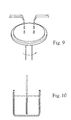
- the thinmesoporous silica film has been formed by the immersion in the precursor solution in the first embodiment, the formation is not restricted to the immersion but a dip coating method may be used as shown in Fig. 10.
- a substrate is brought down perpendicularly to the liquid level of a prepared precursor solution at a speed of 1 mm/s to 10 m/s and is immersed in the solution, and is then held stationarily for 1 second to 1 hour.
- the substrate is perpendicularly brought up again at the speed of 1 mm/s to 10 m/s and is then taken out of the solution.
- a network structure (a cubic structure) is obtained when the molar ratio of the surfactant to the silica derivative, for example, CATB / MSQ is 0.3 to 0.8.
- the molecular ratio is smaller, that is, 0.1 to 0.5, it is possible to obtain an insulating film having a low dielectric constant in which a cylindrical vacancy is oriented.
- the molecular ratio is greater, that is, 0.5 to 2, it is possible to obtain an insulating film having a low dielectric constant in which a layered vacancy is oriented.
- the invention can also be applied to various semiconductor devices using silicon, a high-speed device including a device using a compound semiconductor such as HEMT, a high-frequency device such as a microwave IC, an MFMIS type high integrated ferroelectric memory, a microwave transmission line using a film carrier or a multilayer wiring board.
- a high-speed device including a device using a compound semiconductor such as HEMT, a high-frequency device such as a microwave IC, an MFMIS type high integrated ferroelectric memory, a microwave transmission line using a film carrier or a multilayer wiring board.
Landscapes
- Internal Circuitry In Semiconductor Integrated Circuit Devices (AREA)
- Formation Of Insulating Films (AREA)
- Semiconductor Memories (AREA)
Abstract
It is an object to provide an insulating film having
a very low dielectric constant and a great mechanical
strength. Moreover, it is another object to provide a
semiconductor device capable of reducing both a capacity
between wiring layers and a capacity between wirings
also in microfabrication and an increase in integration
in the semiconductor device. In order to attain the
objects, there is provided an inorganic insulating film
comprising aporous structure having a skeletal structure
in which a vacancy is arranged periodically and a large
number of small holes are included.
Description
The present invention relates to a semiconductor
device and a method of manufacturing the semiconductor
device, and more particularly to an inorganic dielectric
film having a low dielectric constant.
In order to increase a speed and to reduce power
consumption in a semiconductor device, it is an important
object to decrease the dielectric constant of an
interlayer insulating film. Various designs have been
made in order to decrease the dielectric constant. In
a conventional semiconductor device, there have been
proposed methods of:
In the method (1), however, the fluorine can be added
in an element ratio of approximately several % at most
because the heat resistance of the insulating film is
deteriorated. For this reason, there is a problem in
that a specific dielectric constant can be reduced by
only 10% to 15% as compared with a conventional silica
based interlayer insulating film.
In the method (2), moreover, a moisture resistance
and a mechanical strength are deteriorated more
remarkably as compared with the conventional silica based
inter layer insulating film because of an organic material.
Consequently, there is a problem in that the reliability
of a semiconductor device is deteriorated.
In the method (3), furthermore, a porous structure
is random. Therefore, the mechanical strength of an
interlayer insulating film is remarkably reduced so that
the interlayer insulating film is apt to be broken in
packaging. For this reason, the reliability of the
semiconductor device is deteriorated.
In many cases, moreover, the porous structure is
not closed. If the porous structure is not closed, the
moisture resistance of the interlayer insulating film
is remarkably reduced so that the reliability of the
semiconductor device is deteriorated.
With microfabrication and an increase in
integration in a semiconductor device, furthermore, a
capacity between wirings raises serious problems in
addition to a capacity between wiring layers.
In the conventional insulating film, thus, a
dielectric constant cannot fully be decreased.
Moreover, there is a problem in that a mechanical strength
cannot sufficiently be obtained.
The invention has been made in consideration of the
actual circumstances and has an object to provide an
insulating film having a low dielectric constant and
a great mechanical strength.
Furthermore, the invention has an object to provide
a semiconductor device capable of reducing both a
capacity between wiring layers and a capacity between
wirings in microfabrication and an increase in
integration in the semiconductor device.
The invention provides a semiconductor device
comprising an inorganic insulating film formed on a
surface of a substrate and having a periodic porous
structure which includes vacancies having two kinds of
different sizes or more, at least the vacancy having
a first size being arranged periodically.
Moreover, it is desirable that the inorganic
insulating film should include the vacancies having first
and second sizes, the vacancy having the second size
being arranged randomly.
Furthermore, it is desirable that the inorganic
insulating film should have a composite periodic porous
structure which includes the vacancies having first and
second sizes, both of the vacancies having the first
and second sizes being arranged periodically.
According to such a structure, there are included
the vacancies in various sizes to have the periodic porous
structure in which at least the vacancy having the first
size is arranged periodically. Consequently, more
vacancies can be included. The dielectric constant of
air is low. Therefore, the dielectric constant can be
reduced considerably and the dielectric constant of the
insulating film can be reduced extremely. Moreover,
there are plural kinds of periodic porous structures.
Therefore, the opening portions of pores can be closed
each other in the domain so that a mechanical strength
can be increased. Thus, it is possible to obtain an
insulating film having a high reliability.
Moreover, it is desirable that the inorganic
insulating film should be obtained by repetitively
arranging a first porous structure domain comprising
a skeletal structure in which a cylindrical vacancy is
arranged periodically and a large number of small holes
are included and a second porous structure domain
comprising a skeletal structure in which a layered
vacancy is arranged periodically in a perpendicular
direction to the surface of the substrate and a large
number of small holes are included.
According to such a structure, the skeletal
structure having the small holes is employed, more
vacancies can be included and the dielectric constant
can further be reduced. By repetitively arranging the
first porous structure domain having the cylindrical
vacancy provided periodically and the second porous
structure domain having the layered vacancy provided
periodically in a perpendicular direction to the surface
of the substrate, moreover, the vacancy can have such
a closed structure as to have no opening portion for
an upper wiring and a lower wiring in the case in which
the inorganic insulating film is particularly used as
an interlayer insulating film. Thus, the inorganic
insulating film can serve as a thin film having a low
dielectric constant which is excellent in a moisture
resistance, has a high reliability and is effective.
Moreover, it is possible to obtain a uniform electrical
characteristic.
Furthermore, the porous structure is oriented in
a direction which is varied for each domain.
Consequently, the opening portions of the vacancies can
be closed each other. Thus, it is possible to obtain
a thin film which has a great moisture resistance to
be almost equivalent to the moisture resistance of a
minute film, is also excellent in a mechanical strength
because of the periodic structure and has an ultimately
low dielectric constant. Moreover, a space between
layers is supported on the adjacent layers.
Consequently, the layered periodic porous shape to be
usually supposed to be unstable can be constructed stably
with a great mechanical strength.
In addition, it is desirable that the inorganic
insulating film should be obtained by repetitively
laminating, in parallel with the surface of the substrate,
a first porous structure domain layer comprising a
skeletal structure in which a cylindrical vacancy is
arranged periodically and a large number of small holes
are included and a second porous structure domain layer
in which a layered vacancy is arranged periodically in
parallel with the surface of the substrate and a large
number of small holes are included.
According to such a structure, in addition to the
effects described above, in the case in which the
inorganic insulating film is to be particularly used
as an interlayer insulating film, the vacancy can have
such a closed structure as to have no opening portion
with respect to the upper wiring and the lower wiring.
Thus, the inorganic insulating film can serve as a thin
film having a low dielectric constant which is excellent
in a moisture resistance, has a very high reliability
and is effective.
Moreover, it is desirable that the inorganic
insulating film should be an interlayer insulating film
provided between a semiconductor substrate or a first
layer wiring conductor formed on the semiconductor
substrate and a second layer wiring conductor.
According to such a structure, the insulating film
having a low capacity can be formed. Therefore, a
parasitic capacitance can be reduced and the speed of
a semiconductor device can be increased.
It is desirable that the interlayer insulating film
should include a first interlayer insulating film region
which is formed on the first layer wiring conductor and
has a contact hole to come in contact with the first
layer wiring conductor and a second interlayer insulating
film to be filled in a wiring region of the second layer
wiring conductor formed on the first interlayer
insulating film, the first interlayer insulating film
being constituted by a second porous structure domain
having a skeletal structure in which a layered vacancy
is arranged periodically and a large number of small
holes are included.
According to such a structure, there is constituted
the second porous structure domain having the skeletal
structure in which the layered vacancy is arranged
periodically in a region surrounding the contact hole
and a large number of small holes are provided.
Consequently, it is possible to further reduce the
capacity between the layers.
Moreover, it is desirable that the interlayer
insulating film should include a first interlayer
insulating film formed on the first layer wiring
conductor and having a contact hole to come in contact
with the first layer wiring conductor, and a second
interlayer insulating film to be filled in a wiring region
of the second layer wiring conductor formed on the first
interlayer insulating film, the first interlayer
insulating film being constituted by a second porous
structure domain having a skeletal structure in which
a layered vacancy is arranged periodically and a large
number of small holes are included and the second
interlayer insulating film being constituted by a first
porous structure domain having a skeletal structure in
which a cylindrical vacancy is arranged periodically
and a large number of small holes are included.
According to such a structure, there is constituted
the second porous structure domain having the skeletal
structure in which the layered vacancy is arranged
periodically in the region surrounding the contact hole
and a large number of small holes are provided.
Consequently, the capacity between the layers can be
reduced considerably. On the other hand, the
cylindrical vacancy is arranged in a line direction in
an upper layer wiring region constituting an insulating
film between lines. Therefore, a capacity in the line
direction can be reduced more considerably. Moreover,
it is desirable to use the first porous structure domain
in which the direction of the array of the cylindrical
vacancy is orientated in parallel with the direction
of a wiring. Consequently, it is possible to provide
a semiconductor device having a high reliability without
a problem of a short circuit between the wirings.
Moreover, it is desirable that the interlayer
insulating film should include a first interlayer
insulating film formed on the first layer wiring
conductor and having a contact hole to come in contact
with the first layer wiring conductor, and a second
interlayer insulating film to be filled in a wiring region
of the second layer wiring conductor formed on the first
interlayer insulating film, the first interlayer
insulating film being constituted by a second porous
structure domain having a skeletal structure in which
a layered vacancy formed in parallel with the surface
of the substrate is arranged periodically and a large
number of small holes are included and the second
interlayer insulating film being constituted by a third
porous structure domain having a skeletal structure in
which a layered vacancy formed almost perpendicularly
to the surface of the substrate is arranged periodically
and a large number of small holes are included.
According to such a structure, there is constituted
the second porous structure domain having the skeletal
structure in which the layered vacancy is arranged
periodically in the region surrounding the contact hole
in parallel with the surface of the substrate and a large
number of small holes are included. Consequently, the
capacity between the layers can be reduced considerably.
On the other hand, the layered vacancy is arranged
periodically almost perpendicularly to the surface of
the substrate in an upper layer wiring region
constituting the insulating film between lines.
Therefore, a capacity in the line direction can be reduced
still more. Moreover, it is possible to provide a
semiconductor device having a high reliability without
a problem of a short circuit between wirings.
In a method of manufacturing a semiconductor device
according to the invention, the step of manufacturing
an interlayer insulating film comprises the step of
generating a precursor solution to contain a silica
derivative including a siloxane skeleton having a
six-membered ring or more and a surfactant and to have
such a composition ratio that a vacancy is arranged
periodically, the precrosslinking step of raising a
temperature of the precursor solution to start a
crosslinking reaction, the contact step of causing the
precursor solution starting to be crosslinked at the
precrosslinking step to come in contact with a surface
of a substrate, and the step of burning the substrate
with which the precursor solution is caused to come in
contact and decomposing and removing the surfactant,
thereby forming an insulating film.
According to such a method, the silica derivative
including a siloxane skeleton having a six-membered ring
or more is used. Therefore, the skeletal structure
itself is formed to have small holes. Thus, it is
possible to further reduce the dielectric constant while
maintaining the mechanical strength.
In a method of manufacturing a semiconductor device
according to the invention, moreover, the step of
manufacturing an interlayer insulating film comprises
the step of generating a precursor solution to contain
a silica derivative including a siloxane skeleton having
a six-membered ring or more and a surfactant and to have
such a composition ratio that a vacancy is arranged
periodically, the contact step of causing the precursor
solution to come in contact with a surface of a substrate,
the precrosslinking step of raising a temperature of
the precursor solution to start a crosslinking reaction,
and the step of burning the substrate and decomposing
and removing the surfactant, thereby forming an
insulating film.
According to such a method, the silica derivative
including a siloxane skeleton having a six-membered ring
or more is used. Therefore, the skeletal structure
itself is formed to have small holes. Thus, it is
possible to further reduce the dielectric constant while
maintaining the mechanical strength.
Furthermore, the invention provides a method
comprising the step of generating a first precursor
solution to contain a silica derivative including a
siloxane skeleton having a six-membered ring or more
and a surfactant and to have such a first composition
ratio that a vacancy is arranged periodically, the step
of generating a second precursor solution to contain
a silica derivative including a siloxane skeleton having
a six-membered ring or more and a surfactant and to have
such a second composition ratio that a vacancy is arranged
periodically, the precrosslinking step of raising
temperatures of the first and second precursor solutions
to start a crosslinking reaction, the contact step of
causing the firstandsecondprecursorsolutions starting
to be crosslinked at the precrosslinking step to come
in contact with a surface of a substrate, and the step
of burning the substrate with which the first and second
precursor solutions are caused to come in contact and
decomposing and removing the surfactant, thereby forming
an insulating film.
According to such a structure, it is possible to
further reduce the dielectric constant while maintaining
the mechanical strength. Thus, it is possible to provide
an insulating film having a very high controllability,
a great mechanical strength and an ultimately low
dielectric constant. Moreover, it is possible to easily
form the interlayer insulating film having two kinds
of different periodic structures or more, for example,
the interlayer insulating film obtained by repetitively
laminating, in parallel with the surface of the substrate,
the first porous structure domain layer having the
cylindrical vacancy arranged periodically and the second
porous structure domain layer having the layered vacancy
arranged periodically in parallel with the surface of
the substrate.
Moreover, the formation can be carried out at a low
temperature. Also in case of use for the interlayer
insulating film of an integrated circuit, therefore,
it is possible to form an insulating film having a high
reliability without influencing a substrate. The
insulating film can be formed without executing the
heating step at 500°C or more. Also in the case in which
an aluminum wiring is to be used, therefore, the invention
can be applied.
Furthermore, the insulating film can be formed by
the contact of a liquid. Consequently, it is also
possible to form a pattern with high precision in a minute
region. Thus, the reliability can be enhanced.
Moreover, it is possible to properly change the
degree of a vacancy by regulating the concentration of
the precursor solution. Thus, it is possible to form
an insulating thin film having a desirable dielectric
constant with a very high workability.
Furthermore, the method according to the invention
is characterized in that the first and second precursor
solutions are caused to come in contact with the surface
of the substrate and the precrosslinking reaction is
then started.
According to the invention, it is possible to form
the inorganic insulating film in which the vacancy is
formed with two kinds of periodicities or more easily
and efficiently.
It is desirable that the substrate should be
repetitively immersed sequentially in the first and
second precursor solutions at the contact step.
According to such a structure, it is possible to
form, with a high productivity, the insulating film
having a low dielectric constant in which different
porous structure domains are laminated.
Moreover, it is desirable that the contact step
should include the step of immersing the substrate in
the first precursor solution and pulling up the substrate
at a desirable speed and the step of immersing the
substrate in the second precursor solution and pulling
up the substrate at a desirable speed.
Furthermore, it is desirable that the first and
second precursor solutions should be repetitively
applied sequentially onto the substrate at the contact
step.
In addition, it is desirable that the contact step
should be the spin coating step of dropping the first
and second precursor solutions onto the substrate and
rotating the substrate.
According to such a structure, the thickness of a
film and a vacancy rate can easily be regulated and the
insulating film having a low dielectric constant can
be formed with a high productivity.
In the method according to the invention, moreover,
it is possible to enhance the degree of the vacancy still
more by selecting the silica derivative.
In the drawings, 1S denotes a silicon substrate,
12 denotes a first wiring layer, 13a denotes a first
interlayer insulating film, 13b denotes a second
interlayer insulating film, 13S denotes a second
interlayer insulating film, 14 denotes a second wiring
layer, H denotes a contact hole, h denotes a small hole,
1 denotes a silicon substrate, 2 denotes an isolating
film, 3 denotes a gate insulating film, 4 denotes a gate
electrode, 5 denotes a source region, 6 denotes a drain
region, 7 denotes an insulating film, 8 denotes a contact
hole, 9 denotes a lower electrode, 10 denotes a
ferroelectric film, and 11 denotes an upper electrode.
A semiconductor device and a method of manufacturing
the semiconductor device according to an embodiment of
the invention will be described in detail with reference
to the drawings.
As a first embodiment of the invention, description
will be given to a semiconductor device having a
multilayer wiring structure using, as an interlayer
insulating film, a thin film having a low dielectric
constant which comprises a skeletal structure including
a large number of small holes.
As shown in Fig. 1, the semiconductor device is
characterized in that an interlayer insulating film is
constituted by an insulating film having a low dielectric
constant in a two-layer structure, a first interlayer
insulating film 13a having a contact hole H to come in
contact with a first wiring layer 12 is constituted by
a second porous structure domain having a skeletal
structure in which a layered vacancy is arranged
periodically in parallel with the surface of a substrate
and a large number of small holes are included, and a
second interlayer insulating film 13b to be filled in
the wiring region of a second wiring layer 14 on the
upper layer side which is formed on the first interlayer
insulating film 13a is constituted by a first porous
structure domain having a skeletal structure in which
a cylindrical vacancy is arranged periodically and a
large number of small holes are included.
More specifically, the lower layer side of the
interlayer insulating film to be formedbetween the first
wiring layer 12 and the second wiring layer 14 which
are provided on the surface of an element region
surrounded by an isolating film (not shown) formed on
the surface of a silicon substrate 1S is set to be the
first interlayer insulating film 13a having a skeletal
structure in which a layered vacancy is arranged
periodically in parallel with the surface of the
substrate and a large number of small holes h are included,
and the second interlayer insulating film 13b to be formed
as a line insulating film in the wiring pattern region
of the second wiring layer on the upper layer side is
constituted by the first porous structure domain having
a skeletal structure in which a cylindrical vacancy is
arranged periodically and a large number of small holes
are included.
Although other portions are neither shown nor
described, they have ordinary structures.
Referring to Figs. 2(a) to 2(d), a process for
manufacturing the interlayer insulating film will be
described.
As shown in Fig. 2(a), first of all, a desirable
semiconductor region is formed on the surface of a silicon
substrate 1s and a first wiring layer is thus formed
by an ordinary method.
Subsequently, a thin mesoporous silica film
comprising a second periodic porous structure domain
in which a layered vacancy is arranged periodically in
parallel with the surface of the substrate is formed
in parallel with the surface of the substrate by the
method according to the invention (Fig. 2(b)).
More specifically, as shown in Fig. 3(a), cation
type cetyltrimethyl ammonium bromide (CTAB :
C16H33N+(CH3)3Br-) to be a surfactant, hydrogen
silosesquioxane (HSQ : Hydrogen silosesquioxane) to be
a silica derivative, and hydrochloric acid (HCl) to be
an acid catalyst are first dissolved in an H2O / alcohol
mixed solvent, and a precursor solution is prepared in
a mixing vessel. Referring to the molar ratio of
preparation of the precursor solution, 0.5 of the
surfactant, 0.01 of the silica derivative and 2 of the
acid catalyst for 100 of the solvent are mixed, and the
substrate provided with the first wiring layer 12 is
immersed in the mixed solution. As shown in Fig. 3(b),
then, the mixing vessel is closed tightly and is held
at 30°C to 150°C for 1 to 120 hours. Thus, the silica
derivative is polymerized by a hydrolytic
polycondensation reaction (the precrosslinking step)
so that the periodic autoaggregate of the surfactant
is formed.
The autoaggregate forms a spherical micelle
structure (Fig. 4(b)) obtained by agglutinating a
plurality of molecules with C16H33N+(CH3)3Br- to be one
molecule as shown in Fig. 4(a). When the degree of
aggregation is enhanced with an increase in a
concentration (Fig. 4(c)), a layer structure (Fig. 4(d))
having a vacancy oriented is formed.
The substrate is pulled up and is washed and dried,
and is then heated and burned for 3 hours in a nitrogen
atmosphere at 400°C to thermally decompose and remove
the surfactant in a template completely, thereby forming
a pure and thin mesoporous silica film.
As shown in Fig. 2(b), thus, the first interlayer
insulating film 13a having a layered vacancy arranged
in parallel with the surface of the substrate is formed.
Fig. 4(f) is an enlarged explanatory view. An
autoaggregate having a high concentration shown in Fig.
4(d) is formed and is burned. Consequently, it is
possible to form an inorganic insulating film which has
a skeletal structure including a large number of small
holes and is provided with the layered vacancy.
As shown in Fig. 2(c), then, a through hole H is
formed on the first interlayer insulating film 13a and
the second wiring layer 14 is formed by the ordinary
method.
Then, the second interlayer insulating film 13b is
formed. The formation is carried out in the same manner
as in the step of forming the first interlayer insulating
film 13a, and only the composition of the precursor
solution is changed. Referring to the molar ratio of
preparation of the precursor solution, 0.05 of the
surfactant, 0.1 of the silica derivative and 2 of the
acid catalyst for 100 of the solvent are mixed. The
formation is carried out at just the same other steps.
As shown in Fig. 2(d), thus, there is obtained the
second interlayer insulating film 13b having a skeletal
structure in which a cylindrical vacancy is formed
periodically and a large number of small holes are
included.
The concentration of the spherical micelle
structure obtained by agglutinating a plurality of
molecules with C16H33N+(CH3)3Br- to be one molecule is
further increased. Thus, a cylindrical member having
the vacancy arranged is formed and an autoaggregate shown
in Fig. 4(c) is formed and burned. Consequently, there
is obtained the second interlayer insulating film 13b
having the first porous structure domain in which a
cylindrical vacancy is arranged periodically as shown
in an enlarged explanatory view of Fig. 4(e).
Fig. 5 is an explanatory view showing the structure
of a section in this state. As is apparent from Fig.
5, the interlayer insulating film is constituted by the
first interlayer insulating film 13a formed by a porous
thin filmhaving a skeletal structure inwhich the vacancy
is formed like a layer and a large number of small holes
are included and the second interlayer insulating film
13b having a skeletal structure in which the cylindrical
vacancy is arranged periodically and a large number of
small holes are included.
In the semiconductor device having the multilayer
wiring structure thus formed, the interlayer insulating
film constitutes the second porous structure domain in
which the layered vacancy is arranged periodically in
the region surrounding the contact hole H. Consequently,
a capacity between the layers can be reduced. In the
upper layer wiring region constituting the line
insulating film, moreover, the layered vacancy is
arranged in parallel with the wirings. Consequently,
a capacity in a wiring direction can be reduced. In the
line insulating film to be the second interlayer
insulating film on the upper layer side, the direction
of the array of the cylindrical vacancy is oriented in
parallel with the wiring direction of the wiring pattern
of the second wiring layer 14. Therefore, it is possible
to provide a semiconductor device having a high
reliability without a problem of a short circuit between
wirings.
While the interlayer insulating film is constituted
by the insulating film having a low dielectric constant
in the two-layer structure, and the lower layer side
is constituted by the second porous structure domain
having the layered vacancy arranged periodically in
parallel with the surface of the substrate and the upper
layer side is constituted by the first porous structure
domain having the cylindrical vacancy arranged
periodically in the first embodiment, the upper layer
side may be constitutedby a third porous structure domain
to be provided perpendicularly to the surface of the
substrate in parallel with a main wiring in place of
the cylindrical vacancy.
Fig. 6 shows the structure. More specifically, as
shown in Fig. 6, the semiconductor device is
characterized in that an interlayer insulating film is
constituted by an insulating film having a low dielectric
constant in a two-layered structure, a first interlayer
insulating film 13a having a contact hole H to come in
contact with a first wiring layer 12 is constituted by
a second porous structure domain having a skeletal
structure in which a layered vacancy is arranged
periodically in parallel with the surface of a substrate
and a large number of small holes are included, and a
second interlayer insulating film 13S to be filled in
the wiring region of a second wiring layer 14 on the
upper layer side which is formed on the first interlayer
insulating film 13a is constituted by the third porous
structure domain in which a layered vacancy to be almost
perpendicular to the surface of the substrate is arranged
periodically.
More specifically, the lower layer side of the
interlayer insulating film to be formedbetween the first
wiring layer 12 and the second wiring layer 14 which
are provided on the surface of an element region
surrounded by an isolating film (not shown) formed on
the surface of a silicon substrate 1s is set to be the
first interlayer insulating film 13a in which a layered
vacancy is arranged periodically in parallel with the
surface of the substrate, and the second interlayer
insulating film 13S to be formed as a line insulating
film in the wiring pattern region of the second wiring
layer on the upper layer side is constituted by the third
porous structure domain to be provided perpendicularly
to the surface of the substrate in parallel with the
main wiring.
Other portions are neither shown nor described and
are formed in just the same manner as those in the first
embodiment.
According to such a structure, a large number of
vacancies are included, and furthermore, the skeletal
structure having a large number of small holes is employed.
Therefore, it is possible to more reduce a capacity
between lines. Furthermore, the wiring is provided in
parallel with the main wiring. Consequently, a
multilayered insulating wall is present between the
wirings and a short circuit between the wirings can also
be prevented better.
As a third embodiment of the invention, description
will be given to an FRAM using a thin film having a low
dielectric constant as an interlayer insulating film.
As shown in Fig. 7(a) , the FRAM comprises a switching
transistor formed in an element region surrounded by
an isolating film 2 formed on the surface of a silicon
substrate 1 and a ferroelectric capacitor and is
characterized in that a thin film 7 having a low dielectric
constant according to the invention is used as an
interlayer insulating film between the switching
transistor and a lower electrode 9 of the ferroelectric
capacitor in the invention. The thin film having a low
dielectric constant is characterized by a first porous
structure domain 7c having a skeletal structure in which
a cylindrical vacancy is arranged periodically and a
large number of small holes h are included as shown in
an enlarged perspective view illustrating a main part
in Fig. 7(b).
According to such a structure, in addition to the
effects described above, in the case in which the thin
film is particularly used as the interlayer insulating
film, the vacancy can have such a closed structure as
to have no opening portion with respect to an upper layer
wiring and a lower layer wiring. Consequently, it is
possible to produce the advantages of a thin film having
a low dielectric constant which is excellent in a moisture
resistance, has a very high reliability and is effective.
Others are formed by an ordinary method. The
switching transistor comprises a gate electrode formed
on the surface of the silicon substrate 1 through a gate
insulating film 3, and a source region 5 and a drain
region 6 which are formed to interpose the gate electrode
therebetween, and the lower electrode 9 is connected
to the drain region 6 through a contact 8, while a source
- drain region is connected to a bit line BL.
On the other hand, a ferroelectric capacitor is
constituted by interposing a ferroelectric thin film
10 comprising PZT between the lower electrode 9 and an
upper electrode 11.
Referring to Figs. 8 (a) to 8(d), description will
be given to a process for manufacturing the FRAM.
By an ordinary method, first of all, a gate electrode
4 is formed on the surface of the silicon substrate 1
through the gate insulating film 3 and an impurity is
diffused by using the gate electrode 4 as a mask, thereby
forming the source region 5 and the drain region 6 (Fig.
8(a)).
By the method according to the invention,
subsequently, a thin mesoporous silica film is formed
to include a plurality of periodic porous structure
domains having a cylindrical vacancy oriented in one
direction in parallel with the surface of the substrate
(Fig. 8(b)).
More specifically, as shown in Fig. 3(a), cation
type cetyltrimethyl ammonium bromide (CTAB :
C16H33N+(CH3)3Br-) to be a surfactant, methyl
silsesquioxane (MSQ : Methyl silsesquioxane) to be a
silica derivative, and hydrochloric acid (HCl) to be
an acid catalyst are first dissolved in an H2O / alcohol
mixed solvent, and a precursor solution is prepared in
a mixing vessel. Referring to the molar ratio of
preparation of the precursor solution, there are prepared
a first precursor solution mixing 0.05 of the surfactant,
0.1 of the silica derivative and 2 of the acid catalyst
for 100 of the solvent and a second precursor solution
mixing 0.5 of the surfactant, 5 of the silica derivative
and 2 of the acid catalyst for 100 of the solvent. As
shown in Fig. 9, the first and second precursor solutions
thus formed are dropped from respective nozzles onto
the surface of the substrate 1 mounted on a spinner and
a rotation is carried out at 500 to 5000 rpm so that
a thin mesoporous silica film is obtained. The silica
derivative is held at 30°C to 150°C for 1 to 120 hours
and is thereby polymerized by a hydrolytic
polycondensation reaction (the precrosslinking step),
resulting in the formation of a thin mesoporous silica
film having the periodic autoaggregate of the surfactant
to be a template. The precrosslinking step is desirably
carried out at 60°C to 120°C, and more desirably, at 70°C
to 90°C for approximately 12 to 72 hours.
In the samemanner as in the first embodiment, finally,
burning is carried out to thermally decompose and remove
the surfactant completely. Thus, a pure and thin
mesoporous silica film is formed.
While the thin film 7 having a low dielectric constant
according to the embodiment of the invention is thus
formed, it is to be actually formed in two stages in
order to provide the bit line BL. It is also possible
to form an interlayer insulating film in a two-layer
structure having different vacancy arrays by using
precursor solutions having different composition ratios
before and after the formation of the bit line BL.
While the precursor solution is applied onto the
surface of the substrate and the precrosslinking is then
carried out in the embodiment, it is also possible to
carry out the precrosslinking and to then apply the
precursor solution onto the surface of the substrate.
According to such a structure, the precursor solutions
are mixed with difficulty and mutual states can be
maintained. Consequently, an interlayer insulating
film having a plurality of periodic porous structures
can be formed more easily.
As shown in Fig. 8(b), then, a contact hole 8 is
formed on the thin film 7 having a low dielectric constant
by an ordinary method. Thereafter, a buried plug
comprising a doped polycrystalline silicon layer in a
high concentration is formed in the contact hole.
Subsequently, iridium is set to be a target and an iridium
oxide layer is formed by using a mixed gas of argon and
oxygen. Furthermore, a platinum layer is formed on the
iridium oxide layer by using platinum as a target. As
shown in Fig. 8(c), thus, the iridium oxide layer having
a thickness of approximately 50 nm and the platinum layer
having a thickness of approximately 200 nm are formed
and are patterned by photolithography. Thus, the lower
electrode 9 is formed.
Next, a PZT film is formed as the ferroelectric film
10 on the lower electrode 9 by a sol-gel method. A mixed
solution of Pb(CH3COO)2 · 3H2O, Zr(t-OC4H9)4 and
Ti(i-OC3H7)4 was used as a starting material. The mixed
solution was subjected to spin coating and was then dried
at 150°C, and was temporarily burned for 30 minutes at
400°C in a dry air atmosphere. This operation was
repeated five times and a heat treatment was carried
out at 700°C or more in an O2 atmosphere. Thus, the
ferroelectric film 10 having a thickness of 250 nm was
formed. In PbZrxTi1-xO3, x is set to be 0.52 (which will
be hereinafter referred to as PZT (52/48)) and a PZT film
is thus formed (Fig. 8(d)).
Furthermore, a laminated film 11 of iridium oxide
and iridium is formed on the ferroelectric film 10 by
sputtering. The laminated film comprising the iridium
oxide layer and the iridium layer is set to be the upper
electrode 11. Herein, the iridium layer and the iridium
oxide layer are formed to have a thickness of 200 nm
in total. Thus, a ferroelectric capacitor can be
obtained and the FRAM shown in Fig. 7 can be formed.
According to such a structure, the interlayer
insulating film is constituted by the thin film having
a low dielectric constant which is formed by a thin
mesoporous silica film. Therefore, the capacity of the
interlayer insulating film can be reduced. Thus, it is
possible to form an FRAM having an excellent switching
characteristic and capable of carrying out a high-speed
operation.
Moreover, the periodic porous structure is used.
Therefore, a mechanical strength can be increased. Thus,
it is possible to obtain an insulating film having a
high reliability. Furthermore, the interlayer
insulating film is constituted by the first porous
structure domain having the skeletal structure in which
the cylindrical vacancy is arranged periodically and
a large number of small holes are included. Consequently,
it is possible to form an insulating film having a low
dielectric constant in which a mechanical strength is
great. Thus, the operating speed of a device can be
increased. Accordingly, theinterlayerinsulating film
can have a long lifetime.
The composition of the first precursor solution is
not restricted to the composition according to the
embodiment but it is desirable that 0.01 to 0.1 of the
surfactant, 0.01 to 0.5 of the silica derivative and
0 to 5 of the acid catalyst for 100 of the solvent should
be used. By using the precursor solution having such
a structure, it is possible to form an insulating film
having a low dielectric constant which includes a
cylindrical vacancy.
Moreover, the composition of the second precursor
solution is not restricted to the composition according
to the embodiment but it is desirable that 0.1 to 10
of the surfactant, 0.5 to 10 of the silica derivative
and 0 to 5 of the acid catalyst for 100 of the solvent
should be used. By using the precursor solution having
such a structure, it is possible to form an insulating
film having a low dielectric constant which includes
a layered vacancy.
Furthermore, cation type cetyltrimethyl ammonium
bromide (CTAB : C16H33N+(CH3)3Br-) has been used as the
surfactant in the embodiment, which is not restricted.
It is apparent that another surfactant may be used.
If an alkali ion such as an Na ion is used as the
catalyst, a semiconductor material is deteriorated.
For this reason, it is desirable that a cation type
surfactant should be used and an acid catalyst should
be used for the catalyst. For the acid catalyst, it is
also possible to use nitric acid (HNO3), sulfuric acid
(H2SO4), phosphoric acid (H3PO4) and H4SO4 as well as HCl.
Moreover, the silica derivative is not restricted
to HSQ or MSQ but is preferably a material including
a siloxane skeleton having a six-membered ring or more.
Furthermore, while the water H2O / alcohol mixed
solvent has been used for the solvent, only the water
may be used.
Moreover, while the nitrogen atmosphere has been
used for a burning atmosphere, the burning may be carried
out under reduced pressure or in the air. It is desirable
that a foaming gas comprising a mixed gas of nitrogen
and hydrogen should be used. Consequently, a moisture
resistance can be enhanced and a leakage current can
be reduced.
In addition, it is possible to properly change a
mixing ratio of the surfactant, the silica derivative,
the acid catalyst and the solvent.
Furthermore, while the prepolymerizing step has
been held at 30°C to 150°C for 1 to 120 hours, 60°C to
120°C is desirable and 90°C is more desirable.
Moreover, while the burning step has been carried
out at 400°C for 1 hour, it may be performed at 300°C
to 500°C for approximately 1 to 5 hours. It is desirable
that 350°C to 450°C should be set.
While the thinmesoporous silica film has been formed
by the immersion in the precursor solution in the first
embodiment, the formation is not restricted to the
immersion but a dip coating method may be used as shown
in Fig. 10.
More specifically, a substrate is brought down
perpendicularly to the liquid level of a prepared
precursor solution at a speed of 1 mm/s to 10 m/s and
is immersed in the solution, and is then held stationarily
for 1 second to 1 hour.
After a desirable time passes, the substrate is
perpendicularly brought up again at the speed of 1 mm/s
to 10 m/s and is then taken out of the solution.
Finally, burning is carried out in the same manner
as in the first embodiment. Consequently, a surfactant
is thermally decomposed and removed completely to form
a pure and thin dual porous silica film.
As a fifth embodiment of the invention, moreover,
it is also effective that small holes are randomly formed
between vacancies arranged periodically as shown in Fig.
11.
It is apparent that the construction of an acquired
structure is changed depending on the ratio of a
surfactant to a silica derivative having a six-membered
ring structure when a precursor solution is to be
prepared.
For example, it is apparent that a network structure
(a cubic structure) is obtained when the molar ratio
of the surfactant to the silica derivative, for example,
CATB / MSQ is 0.3 to 0.8. When the molecular ratio is
smaller, that is, 0.1 to 0.5, it is possible to obtain
an insulating film having a low dielectric constant in
which a cylindrical vacancy is oriented. On the other
hand, when the molecular ratio is greater, that is, 0.5
to 2, it is possible to obtain an insulating film having
a low dielectric constant in which a layered vacancy
is oriented.
While the applying method using the spinner has been
described in the embodiment, it is also possible to apply
a so-called brushing method of carrying out application
by means of a brush.
In addition, while the interlayer insulating film
of the FRAM has been described in the embodiment, the
invention can also be applied to various semiconductor
devices using silicon, a high-speed device including
a device using a compound semiconductor such as HEMT,
a high-frequency device such as a microwave IC, an MFMIS
type high integrated ferroelectric memory, a microwave
transmission line using a film carrier or a multilayer
wiring board.
As described above, according to the invention, it
is possible to easily obtain an insulating film having
a very low dielectric constant with a high
controllability and a great mechanical strength.
Moreover, it is possible to obtain a thin film having
a low dielectric constant which is particularly effective
for an interlayer insulating film.
Claims (16)
- A semiconductor device comprising an inorganic insulating film formed on a surface of a substrate and having a periodic porous structure which includes vacancies having two kinds of different sizes or more, at least the vacancy having a first size being arranged periodically.
- The semiconductor device according to claim 1, wherein the inorganic insulating film includes the vacancies having first and second sizes, the vacancy having the second size being arranged randomly.
- The semiconductor device according to claim 1, wherein the inorganic insulating film has a composite periodic porous structure which includes the vacancies having first and second sizes, both of the vacancies having the first and second sizes being arranged periodically.
- The semiconductor device according to claim 1, wherein the inorganic insulating film is obtained by repetitively laminating, in parallel with the surface of the substrate, a first porous structure domain layer comprising a skeletal structure in which a cylindrical vacancy having the first size is arranged periodically and a large number of small holes are included and a second porous structure domain layer in which a layered vacancy is periodically arranged in parallel with the surface of the substrate and a large number of small holes are included.
- The semiconductor device according to any of claims 1 to 4, wherein the inorganic insulating film is an interlayer insulating film provided between a semiconductor substrate or a first layer wiring conductor formed on the semiconductor substrate and a second layer wiring conductor formed thereon.
- The semiconductor device according to claim 5, wherein the interlayer insulating film includes a first interlayer insulating film which is formed on the first layer wiring conductor and has a contact hole to come in contact with the first layer wiring conductor and a second interlayer insulating film to be filled in a wiring region of the second layer wiring conductor formed on the first interlayer insulating film, the first interlayer insulating film being constituted by a second porous structure domain having a skeletal structure in which a layered vacancy is arranged periodically and a large number of small holes are included.
- The semiconductor device according to claim 5, wherein the interlayer insulating film comprises:a first interlayer insulating film formed on the first layer wiring conductor and having a contact hole to come in contact with the first layer wiring conductor; anda second interlayer insulating film to be filled in a wiring region of the second layer wiring conductor formed on the first interlayer insulating film,the first interlayer insulating film being constituted by a second porous structure domain having a skeletal structure in which a layered vacancy is arranged periodically and a large number of small holes are included and the second interlayer insulating film being constituted by a first porous structure domain having a skeletal structure in which a cylindrical vacancy is arranged periodically and a large number of small holes are included.
- The semiconductor device according to claim 5, wherein the interlayer insulating film comprises:a first interlayer insulating film formed on the first layer wiring conductor and having a contact hole to come in contact with the first layer wiring conductor; anda second interlayer insulating film to be filled in a wiring region of the second layer wiring conductor formed on the first interlayer insulating film,the first interlayer insulating film being constituted by a second porous structure domain having a skeletal structure in which a layered vacancy formed in parallel with the surface of the substrate is arranged periodically and a large number of small holes are included and the second interlayer insulating film being constituted by a third porous structure domain having a skeletal structure in which a layered vacancy formed almost perpendicularly to the surface of the substrate is arranged periodically and a large number of small holes are included.
- A method of manufacturing a semiconductor device, comprising:the step of generating a precursor solution to contain a silica derivative including a siloxane skeleton having a six-membered ring or more and a surfactant and to have such a composition ratio that a vacancy is arranged periodically;the precrosslinking step of raising a temperature of the precursor solution to start a crosslinking reaction;the contact step of causing the precursor solution starting to be crosslinked at the precrosslinking step to come in contact with a surface of a substrate; andthe step of burning the substrate with which the precursor solution is caused to come in contact and decomposing and removing the surfactant, thereby forming an insulating film.
- A method of manufacturing a semiconductor device, comprising:the step of generating a precursor solution to contain a silica derivative including a siloxane skeleton having a six-membered ring or more and a surfactant and to have such a composition ratio that a vacancy is arranged periodically;the contact step of causing the precursor solution to come in contact with a surface of a substrate;the precrosslinking step of raising a temperature of the precursor solution to start a crosslinking reaction;
andthe step of burning the substrate and decomposing and removing the surfactant, thereby forming an insulating film. - A method of manufacturing a semiconductor device, comprising:the step of generating a first precursor solution to contain a silica derivative including a siloxane skeleton having a six-membered ring or more and a surfactant and to have such a first composition ratio that a vacancy is arranged periodically;the step of generating a second precursor solution to contain a silica derivative including a siloxane skeleton having a six-membered ring or more and a surfactant and to have such a second composition ratio that a vacancy is arranged periodically;the precrosslinking step of raising temperatures of the first and second precursor solutions to start a crosslinking reaction;the contact step of causing the first and second precursor solutions starting to be crosslinked at the precrosslinking step to come in contact with a surface of a substrate; andthe step of burning the substrate with which the first and second precursor solutions are caused to come in contact and decomposing and removing the surfactant, thereby forming an insulating film.
- A method of manufacturing a semiconductor device, comprising:the step of generating a first precursor solution to contain a silica derivative including a siloxane skeleton having a six-membered ring or more and a surfactant and to have such a first composition ratio that a vacancy is arranged periodically;the step of generating a second precursor solution to contain a silica derivative including a siloxane skeleton having a six-membered ring or more and a surfactant and to have such a second composition ratio that a vacancy is arranged periodically;the contact step of causing the first and second precursor solutions to come in contact with a surface of a substrate;the precrosslinking step of heating the substrate with which the first and second precursor solutions are caused to come in contact to start a crosslinking reaction; andthe step of burning the substrate and decomposing and removing the surfactant, thereby forming an insulating film.
- The method of manufacturing a semiconductor device according to claim 11 or 12, wherein the substrate is repetitively immersed sequentially in the first and second precursor solutions at the contact step.
- The method of manufacturing a semiconductor device according to claim 11 or 12, wherein the contact step includes the step of immersing the substrate in the first precursor solution and pulling up the substrate at a desirable speed and the step of immersing the substrate in the second precursor solution and pulling up the substrate at a desirable speed.
- The method of manufacturing a semiconductor device according to claim 11 or 12, wherein the first and second precursor solutions are repetitively applied sequentially onto the substrate at the contact step.
- The method of manufacturing a semiconductor device according to claim 11 or 12, wherein the contact step is the spin coating step of dropping the first and second precursor solutions onto the substrate and rotating the substrate.
Applications Claiming Priority (3)
| Application Number | Priority Date | Filing Date | Title |
|---|---|---|---|
| JP2001198963A JP4953523B2 (en) | 2001-06-29 | 2001-06-29 | Semiconductor device and manufacturing method thereof |
| JP2001198963 | 2001-06-29 | ||
| PCT/JP2002/006507 WO2003003450A1 (en) | 2001-06-29 | 2002-06-27 | Semiconductor device and production method therefor |
Publications (2)
| Publication Number | Publication Date |
|---|---|
| EP1408546A1 true EP1408546A1 (en) | 2004-04-14 |
| EP1408546A4 EP1408546A4 (en) | 2008-01-02 |
Family
ID=19036316
Family Applications (1)
| Application Number | Title | Priority Date | Filing Date |
|---|---|---|---|
| EP02743748A Withdrawn EP1408546A4 (en) | 2001-06-29 | 2002-06-27 | SEMICONDUCTOR DEVICE AND METHOD FOR MANUFACTURING THE SAME |
Country Status (7)
| Country | Link |
|---|---|
| US (1) | US7411275B2 (en) |
| EP (1) | EP1408546A4 (en) |
| JP (1) | JP4953523B2 (en) |
| KR (1) | KR100622713B1 (en) |
| CN (1) | CN1261996C (en) |
| TW (1) | TW548861B (en) |
| WO (1) | WO2003003450A1 (en) |
Families Citing this family (3)
| Publication number | Priority date | Publication date | Assignee | Title |
|---|---|---|---|---|
| US7405147B2 (en) * | 2004-01-30 | 2008-07-29 | International Business Machines Corporation | Device and methodology for reducing effective dielectric constant in semiconductor devices |
| JP4657859B2 (en) * | 2005-09-09 | 2011-03-23 | ローム株式会社 | Porous thin film manufacturing method, porous thin film and semiconductor device using the same |
| US20140264271A1 (en) * | 2013-03-18 | 2014-09-18 | National Applied Research Laboratories | Ferroelectric memory device |
Family Cites Families (14)
| Publication number | Priority date | Publication date | Assignee | Title |
|---|---|---|---|---|
| US5494858A (en) * | 1994-06-07 | 1996-02-27 | Texas Instruments Incorporated | Method for forming porous composites as a low dielectric constant layer with varying porosity distribution electronics applications |
| JPH09194298A (en) * | 1995-04-25 | 1997-07-29 | Rikagaku Kenkyusho | Silica-surfactant nanocomposite and method for producing the same |
| US5858457A (en) | 1997-09-25 | 1999-01-12 | Sandia Corporation | Process to form mesostructured films |
| JP3228251B2 (en) * | 1998-12-16 | 2001-11-12 | 日本電気株式会社 | CVD apparatus and semiconductor device manufacturing method using the same |
| US6399177B1 (en) * | 1999-06-03 | 2002-06-04 | The Penn State Research Foundation | Deposited thin film void-column network materials |
| EP1094506A3 (en) * | 1999-10-18 | 2004-03-03 | Applied Materials, Inc. | Capping layer for extreme low dielectric constant films |
| JP4524822B2 (en) * | 1999-10-29 | 2010-08-18 | 株式会社豊田中央研究所 | Method for producing highly crystalline silica mesoporous film |
| US6365266B1 (en) * | 1999-12-07 | 2002-04-02 | Air Products And Chemicals, Inc. | Mesoporous films having reduced dielectric constants |
| JP3578722B2 (en) | 2000-03-17 | 2004-10-20 | 松下電器産業株式会社 | Interlayer insulating film, method for forming the same, and method for forming wiring |
| JP2001351911A (en) * | 2000-04-03 | 2001-12-21 | Ulvac Japan Ltd | Method of forming porous sog film |
| JP4540885B2 (en) * | 2001-06-29 | 2010-09-08 | ローム株式会社 | Manufacturing method of semiconductor device |
| JP2003017483A (en) * | 2001-06-29 | 2003-01-17 | Rohm Co Ltd | Semiconductor device and method of manufacturing the same |
| EP1408539A1 (en) * | 2001-06-29 | 2004-04-14 | Rohm Co., Ltd. | Semiconductor device and production method therefor |
| US6717195B2 (en) * | 2001-06-29 | 2004-04-06 | Rohm Co., Ltd. | Ferroelectric memory |
-
2001
- 2001-06-29 JP JP2001198963A patent/JP4953523B2/en not_active Expired - Fee Related
-
2002
- 2002-06-27 CN CNB028020650A patent/CN1261996C/en not_active Expired - Fee Related
- 2002-06-27 KR KR1020037001316A patent/KR100622713B1/en not_active Expired - Fee Related
- 2002-06-27 US US10/482,628 patent/US7411275B2/en not_active Expired - Fee Related
- 2002-06-27 WO PCT/JP2002/006507 patent/WO2003003450A1/en not_active Ceased
- 2002-06-27 EP EP02743748A patent/EP1408546A4/en not_active Withdrawn
- 2002-06-28 TW TW091114282A patent/TW548861B/en not_active IP Right Cessation
Also Published As
| Publication number | Publication date |
|---|---|
| EP1408546A4 (en) | 2008-01-02 |
| CN1463471A (en) | 2003-12-24 |
| CN1261996C (en) | 2006-06-28 |
| KR100622713B1 (en) | 2006-09-13 |
| US7411275B2 (en) | 2008-08-12 |
| JP2003017560A (en) | 2003-01-17 |
| KR20040014927A (en) | 2004-02-18 |
| TW548861B (en) | 2003-08-21 |
| US20040242020A1 (en) | 2004-12-02 |
| JP4953523B2 (en) | 2012-06-13 |
| WO2003003450A1 (en) | 2003-01-09 |
Similar Documents
| Publication | Publication Date | Title |
|---|---|---|
| EP1482567A1 (en) | Light-emitting device comprising led chip and method for manufacturing this device | |
| US8575040B2 (en) | Low temperature process for polysilazane oxidation/densification | |
| CN101390200A (en) | Highly Selectively Doped Oxide Etchant | |
| US20070164437A1 (en) | Semiconductor device and method of manufacturing the same | |
| US7411275B2 (en) | Semiconductor device comprising an inorganic insulating film and method of manufacturing the same | |
| JP4170219B2 (en) | Semiconductor device manufacturing method and semiconductor device | |
| US7105459B2 (en) | Method for forming thin film | |
| KR100645654B1 (en) | Semiconductor device and manufacturing method thereof | |
| US7375774B2 (en) | Method of manufacturing semiconductor device | |
| KR100253094B1 (en) | Capacitor manufacturing method of semiconductor device and semiconductor capacitor manufactured accordingly | |
| JP2003017485A (en) | Semiconductor device and method of manufacturing the same | |
| JP2003017484A (en) | Semiconductor device and method for manufacturing the same | |
| JP2003017663A (en) | Ferroelectric memory | |
| JP2003017483A (en) | Semiconductor device and method of manufacturing the same | |
| JP2003017486A (en) | Semiconductor device and method of manufacturing the same | |
| JP2006203029A (en) | Manufacturing method of semiconductor device | |
| KR19990060920A (en) | Method for forming charge storage electrode of semiconductor device |
Legal Events
| Date | Code | Title | Description |
|---|---|---|---|
| PUAI | Public reference made under article 153(3) epc to a published international application that has entered the european phase |
Free format text: ORIGINAL CODE: 0009012 |
|
| 17P | Request for examination filed |
Effective date: 20031223 |
|
| AK | Designated contracting states |
Kind code of ref document: A1 Designated state(s): AT BE CH CY DE DK ES FI FR GB GR IE IT LI LU MC NL PT SE TR |
|
| A4 | Supplementary search report drawn up and despatched |
Effective date: 20071204 |
|
| 17Q | First examination report despatched |
Effective date: 20090303 |
|
| STAA | Information on the status of an ep patent application or granted ep patent |
Free format text: STATUS: THE APPLICATION HAS BEEN WITHDRAWN |
|
| 18W | Application withdrawn |
Effective date: 20090604 |