EP1408544A1 - Film thichness measuring monitor wafer - Google Patents
Film thichness measuring monitor wafer Download PDFInfo
- Publication number
- EP1408544A1 EP1408544A1 EP20020701695 EP02701695A EP1408544A1 EP 1408544 A1 EP1408544 A1 EP 1408544A1 EP 20020701695 EP20020701695 EP 20020701695 EP 02701695 A EP02701695 A EP 02701695A EP 1408544 A1 EP1408544 A1 EP 1408544A1
- Authority
- EP
- European Patent Office
- Prior art keywords
- wafer
- film thickness
- monitor
- sic
- film
- Prior art date
- Legal status (The legal status is an assumption and is not a legal conclusion. Google has not performed a legal analysis and makes no representation as to the accuracy of the status listed.)
- Granted
Links
Images



Classifications
-
- H—ELECTRICITY
- H10—SEMICONDUCTOR DEVICES; ELECTRIC SOLID-STATE DEVICES NOT OTHERWISE PROVIDED FOR
- H10P—GENERIC PROCESSES OR APPARATUS FOR THE MANUFACTURE OR TREATMENT OF DEVICES COVERED BY CLASS H10
- H10P74/00—Testing or measuring during manufacture or treatment of wafers, substrates or devices
-
- H—ELECTRICITY
- H10—SEMICONDUCTOR DEVICES; ELECTRIC SOLID-STATE DEVICES NOT OTHERWISE PROVIDED FOR
- H10P—GENERIC PROCESSES OR APPARATUS FOR THE MANUFACTURE OR TREATMENT OF DEVICES COVERED BY CLASS H10
- H10P74/00—Testing or measuring during manufacture or treatment of wafers, substrates or devices
- H10P74/27—Structural arrangements therefor
- H10P74/277—Circuits for electrically characterising or monitoring manufacturing processes, e.g. circuits in tested chips or circuits in testing wafers
-
- H—ELECTRICITY
- H10—SEMICONDUCTOR DEVICES; ELECTRIC SOLID-STATE DEVICES NOT OTHERWISE PROVIDED FOR
- H10P—GENERIC PROCESSES OR APPARATUS FOR THE MANUFACTURE OR TREATMENT OF DEVICES COVERED BY CLASS H10
- H10P90/00—Preparation of wafers not covered by a single main group of this subclass, e.g. wafer reinforcement
- H10P90/19—Preparing inhomogeneous wafers
- H10P90/1904—Preparing vertically inhomogeneous wafers
-
- H—ELECTRICITY
- H10—SEMICONDUCTOR DEVICES; ELECTRIC SOLID-STATE DEVICES NOT OTHERWISE PROVIDED FOR
- H10P—GENERIC PROCESSES OR APPARATUS FOR THE MANUFACTURE OR TREATMENT OF DEVICES COVERED BY CLASS H10
- H10P74/00—Testing or measuring during manufacture or treatment of wafers, substrates or devices
- H10P74/20—Testing or measuring during manufacture or treatment of wafers, substrates or devices characterised by the properties tested or measured, e.g. structural or electrical properties
- H10P74/203—Structural properties, e.g. testing or measuring thicknesses, line widths, warpage, bond strengths or physical defects
Definitions
- the present invention relates to a monitor wafer, in particular, to a film thickness measuring monitor wafer among monitor wafers, which can be used as a monitor wafer even if a surface of the monitor wafer is not polished to the level of the surface roughness of a product Si wafer.
- dummy wafers or monitor wafers are usually mounted on a wafer boat together with the product Si wafers.
- the dummy wafers are added when the product wafers are still insufficient in a specified number of the wafers, or inserted to make a temperature or a gas flow inside a furnace uniform in the CVD process and the like, and therefore, the dummy wafer can not be a final product.
- the monitor wafer is processed by completely the same processes as those for the product Si wafer, to monitor a film thickness of a CVD film or the like which is formed on the product Si wafer, and the number of particles in the furnace. Accordingly, especially the product Si wafers and the monitor wafer are placed on a wafer boat together, and thermal oxidation films or CVD films are formed simultaneously on the surfaces of the product wafers and the monitor wafer through predetermined processing.
- the film thickness measuring monitor wafer is taken out from the boat. Then, a film thickness of the film formed on the monitor wafer is measured with a film thickness measuring instrument to judge whether or not the measured film thickness is within a spec. If it is within the spec, it can be judged that a film having a film thickness within the spec is formed on the product wafer processed at the same time, so that the product wafer can be transferred to a next process.
- a film thickness measuring monitor wafer described above conventionally, an Si wafer made of the same material as the product wafer has been usually used.
- the film is removed by polishing or etching, or a combination of polishing and etching every time when the film thickness measurement is finished, so as to render it reusable.
- a D-poly deposition process for a six-inch wafer a D-poly film having a thickness of 1000 ⁇ is formed on the film thickness measuring monitor wafer in one time. Once formed, the D-poly film is removed with HF + HNO 3 + H 2 O (1 : 8 : 12) to use it as a film thickness measuring monitor wafer again.
- the SiC monitor wafer is a disciform silicon carbide film having a film thickness of about 1 mm formed by a CVD method, has many following advantages written below and practical use of the SiC monitor wafer is promoted due to its prominent economical effect.
- SiC, alumina, quartz, tungsten, molybdenum, and further glassy carbon and sapphire can be cited as a raw material for a monitor wafer for measuring film thickness and the above basic principle can be applied to these materials.
- the object of the present invention is to provide a wafer having a structure of enabling a hard wafer such as an SiC material to be put to practical use as a wafer for monitoring a film thickness.
- the inventors have obtained knowledge that even if surface roughness of a monitor wafer is not equivalent to surface roughness of a product Si wafer, it is sufficient for the monitor wafer so far as the monitor wafer has surface roughness from which reflection intensity (reflection coefficient) necessary for the measurement can be obtained, and when the monitor wafer is allowed to have surface roughness substantially equivalent to the minimum film thickness for a measurable limit thickness of films to be measured, monitoring of film thickness can be appropriately performed, and have reach the present invention.
- a film thickness measuring monitor wafer relating to the present invention comprises a wafer having an average surface roughness Ra of at least one surface of the wafer being set to be equivalent or less to a film thickness of a film deposited on an Si wafer to be measured.
- a film thickness measuring monitor wafer relating to the present invention comprises a wafer having an average surface roughness Ra of at least one surface of the wafer being able to set to be a close value less than an upper limit value when the minimum film thickness among several types of films deposited on an Si wafer to be measured is taken as the upper limit value
- a film thickness measuring monitor wafer relating to the present invention comprises a wafer having an upper limit value of the average film roughness of at least one surface of the monitor wafer preferably being set to be about 400 times as large as the average surface roughness of a product Si wafer.
- the average surface roughness of the above-described monitor wafer is preferably set to be 0.08 ⁇ m or less, more preferably 0.02 ⁇ m or less.
- FIG. 1 shows an example of a manufacturing process to form a monitor wafer 40 relating to the embodiment using SiC as a material.
- a SiC wafer such as calcinations of SiC powders, silicon-carbonization of carbon with Si gas, and the like
- this figure shows a manufacturing process by a CVD method.
- a circular graphite base material 42 made of high purity graphite and having a predetermined size is prepared in accordance with the size of an SiC monitor wafer 40 which will be manufactured (FIG. 1 (1)).
- the circular graphite base material 42 is put in a CVD apparatus and the inside of the apparatus (furnace) is heated to and kept at a predetermined temperature, for instance, 1000 to 1600°C.
- the inside of the furnace is set to a predetermined pressure, for instance, 100 Torr.
- SiCl 4 and C 3 H 8 which are raw materials of SiC are supplied to the CVD apparatus in an amount of 5 to 20 vol.% respectively with hydrogen gas (H 2 ) as a carrier gas.
- H 2 hydrogen gas
- an SiC layer (silicon carbide layer) 44 is deposited on the surface of the graphite base material 42, and this deposition processing is continued till the film thickness comes to 0.1mm to about 1 mm (FIG. 1(2)).
- the graphite base material 42 on the surface of which a film of SiC layer 44 is formed is taken out from the CVD apparatus, and the peripheral surface thereof is removed by a mechanical grinding process so that the peripheral surface of the graphite base material 42 is exposed (FIG. 1(3)).
- the graphite base material 42 sandwiched by SiC films is put into a furnace at 900 to 1400°C while supplying oxygen thereto so that two sheets of SiC monitor wafer 40 are obtained by burning to remove the graphite base material 42 under an oxidation atmosphere (FIG. 1(4)).
- the SiC monitor wafer 40 is polished and, at the same time, the peripheral edge portions are chamfered.
- the monitor wafer is generally surface-polished in the same manner as an ordinary silicon wafer.
- the SiC monitor wafer 40 is polished by polishing with diamond abrasive grains, and the average surface roughness Ra is set as will be described below.
- At least the average surface roughness Ra on one surface of the SiC wafer 40 is set to be substantially equivalent to or smaller than the film thickness of the film deposited on the Si wafer which is an object wafer for the measurement.
- an insulating oxide film, polycrystalline silicon film or the like is deposited so as to have a film thickness of, for instance, 250 ⁇ , 500 ⁇ , 1000 ⁇ or the like.
- the surface roughness Ra of the above-described SiC wafer 40 is set to be at least substantially equivalent to or smaller than the thickness to be the minimum film thickness.
- the average surface roughness Ra given to the SiC wafer 40 is set to be Ra ⁇ 0.025 ⁇ m.
- the average surface roughness of the product wafer (Si wafer) is Ra ⁇ 0.0002 ⁇ m, and corresponding to this, the upper limit value of the surface roughness Ra of the SiC monitor wafer 40 may be set to be Ra ⁇ 0.08 ⁇ m which is 400 times of the average surface roughness of the product wafer.
- the SiC monitor wafer 40 can be practically used just as a film thickness monitor.
- Ra ⁇ 0.08 ⁇ m is set to be the upper limit value, it is needless to say that the surface roughness is desirably as small as possible. Therefore, it is desirable that the upper limit value Ra is set to be 0.02 ⁇ m, which is 100 times as much as the average surface roughness of the product wafer.
- the following is a concrete example in which the Si wafer and the SiC wafer are subjected to film deposition processing respectively, and the SiC wafer is confirmed to be applicable as a film thickness monitor.
- An Si monitor and an SiC monitor are used as a wafer.
- Polycrystalline silicon is vapor-deposited simultaneously on the Si monitor wafer and the SiC monitor wafer so that different film thickness order of 2000 ⁇ , 1400 ⁇ ,and 700 ⁇ can be obtained, and the experiment is carried out for each one batch.
- the thickness measurement result of the vapor-deposited films is shown in Tables 1 and 2 below.
- the measurement result is obtained using NanoSpec 8000XSE manufactured by Nanometrix Corp. Si (unit: angstrom) No. 1 No. 2 No. 3 No. 4 No. 5 No. 6 1998 2039 2032 2052 2049 2020 1429 1461 1466 1463 1465 1450 693 705 706 707 704 701 SiC (unit: angstrom) No.1 No. 2 No. 3 No. 4 No. 5 No. 6 2011 2035 2022 2036 2027 2023 1435 1458 1455 1460 1451 1448 687 700 701 709 698 703
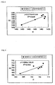
- FIG. 2 is a plotted graph showing measured film thickness of No. 1 taking the Si wafer on the horizontal axis and the SiC wafer on the vertical axis. Its approximation degree is 0.9998, and the graph clearly shows that an SiC wafer can be used as a film thickness measuring monitor wafer.
- FIG. 3 to FIG. 5 are graphs prepared for each film thickness.
- An 8-inch CVD-SiC black mirror surface wafer is used as a film thickness monitor wafer, and a Poly-Si film is deposited on it and on a product Si wafer together.
- a film thickness at the central portion on the mirror-surface side (front surface) can be measured, a film thickness of the outer peripheries of the mirror-surface side and the matte finish surface (rear surface) cannot be measured.
- the surface roughness of the monitor wafers in the slit Nos. 1, 3, 5, 7 of the wafer carrier case are measured.
- FIG. 6 is a view explaining the method of measuring the surface roughness of a monitor wafer.
- the measurement is carried out in such a manner that an orienteering flat portion is put toward downside, and the portions at the center in the radial direction of the wafer, 50 mm from the center, and 90 mm from the center are measured in the circumferential direction at intervals of 45-degree pitch.
- the measurement is performed on both sides of front face and back face, taking the mirror-face side as the front face.
- a contact-type surface roughness meter SURFCOM 120A manufactured by TOKYO SEIMITSU CO., LTD is used for the measurement of the surface roughness.
- the measurement result is shown in the following table. unit: ⁇ m Angle Slit No.
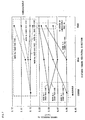
- FIG. 7 The above-described measurement result is shown in FIG. 7 in a graph.
- a solid line indicates the front face side
- a broken line indicates the back face side. From this figure, it is found that the front face side is smaller in surface roughness than that of the back face side, and the surface roughness is getting larger from the center of the wafer toward the outer periphery as a whole.
- the film thickness measuring monitor wafer relating to the present invention has a structure that the average surface roughness Ra of at least one surface of a wafer is set to be substantially eqivalent to the film thickness to be deposited on an Si wafer to be measured, it can be used practically as a film thickness monitor wafer without polishing the hard film thickness measuring wafer having chemical resistance to a degree of a product Si wafer, so that it has an effect of providing a film thickness measuring monitor wafer which can reduce the polishing cost and can be used semi-permanently.
- the monitor wafer relating to the present invention can be applied to a deposition processing of a wafer in a semiconductor manufacturing process.
Landscapes
- Testing Or Measuring Of Semiconductors Or The Like (AREA)
- Chemical Vapour Deposition (AREA)
Abstract
Description
| Si (unit: angstrom) | |||||
| No. 1 | No. 2 | No. 3 | No. 4 | No. 5 | No. 6 |
| 1998 | 2039 | 2032 | 2052 | 2049 | 2020 |
| 1429 | 1461 | 1466 | 1463 | 1465 | 1450 |
| 693 | 705 | 706 | 707 | 704 | 701 |
| SiC (unit: angstrom) | |||||
| No.1 | No. 2 | No. 3 | No. 4 | No. 5 | No. 6 |
| 2011 | 2035 | 2022 | 2036 | 2027 | 2023 |
| 1435 | 1458 | 1455 | 1460 | 1451 | 1448 |
| 687 | 700 | 701 | 709 | 698 | 703 |
| unit: µm | |||||||||
| Angle | Slit No. | ||||||||
| 1 | 3 | 5 | 7 | ||||||
| Front | Back | Front | Back | Front | Back | Front | Back | ||
| Center | 0.06 | 0.10 | 0.08 | 0.10 | 0.06 | 0.10 | 0.08 | 0.10 | |
| 50 mm from | 0 degree | 0.08 | 0.10 | 0.04 | 0.10 | 0.06 | 0.10 | 0.10 | 0.12 |
| 45 degree | 0.08 | 0.10 | 0.10 | 0.10 | 0.06 | 0.12 | 0.08 | 0.10 | |
| 90 degree | 0.06 | 0.10 | 0.08 | 0.10 | 0.06 | 0.10 | 0.08 | 0.12 | |
| 135 degree | 0.08 | 0.10 | 0.08 | 0.10 | 0.06 | 0.10 | 0.08 | 0.10 | |
| 180 degree | 0.08 | 0.10 | 0.08 | 0.10 | 0.06 | 0.10 | 0.08 | 0.10 | |
| 225 degree | 0.06 | 0.10 | 0.06 | 0.10 | 0.06 | 0.10 | 0.10 | 0.10 | |
| 270 degree | 0.08 | 0.12 | 0.06 | 0.10 | 0.06 | 0.10 | 0.08 | 0.10 | |
| 315 degree | 0.08 | 0.10 | 0.06 | 0.10 | 0.06 | 0.10 | 0.08 | 0.10 | |
| average | 0.08 | 0.10 | 0.07 | 0.10 | 0.06 | 0.10 | 0.09 | 0.11 | |
| 90 mm from | 0 degree | 0.10 | 0.10 | 0.08 | 0.10 | 0.06 | 0.14 | 0.10 | 0.14 |
| 45 degree | 0.08 | 0.10 | 0.08 | 0.10 | 0.08 | 0.12 | 0.08 | 0.12 | |
| 90 degree | 0.08 | 0.10 | 0.06 | 0.10 | 0.06 | 0.10 | 0.10 | 0.12 | |
| 135 degree | 0.10 | 0.10 | 0.08 | 0.10 | 0.06 | 0.10 | 0.08 | 0.10 | |
| 180 degree | 0.08 | 0.10 | 0.06 | 0.10 | 0.10 | 0.10 | 0.08 | 0.10 | |
| 225 degree | 0.08 | 0.10 | 0.08 | 0.10 | 0.10 | 0.12 | 0.10 | 0.12 | |
| 270 degree | 0.08 | 0.10 | 0.08 | 0.10 | 0.10 | 0.10 | 0.10 | 0.12 | |
| 315 degree | 0.10 | 0.10 | 0.08 | 0.08 | 0.10 | 0.10 | 0.08 | 0.12 | |
| average | 0.09 | 0.10 | 0.08 | 0.10 | 0.08 | 0.11 | 0.09 | 0.12 |
In FIG. 7, a solid line indicates the front face side, and a broken line indicates the back face side. From this figure, it is found that the front face side is smaller in surface roughness than that of the back face side, and the surface roughness is getting larger from the center of the wafer toward the outer periphery as a whole. It is turned out that the central portion on the front side where the film thickness was measurable is smaller in surface roughness than other portions, the film thickness is measurable on a portion having a value equal to or smaller than surface roughness Ra = 0.08 µm, which is the surface roughness value for the central portion, and when the surface roughness is larger than Ra = 0.08 µm, the measurement is unstable, and further when Ra = 0.1 µm or more, it was unmeasurable.
Claims (4)
- A film thickness measuring monitor wafer, comprising:a wafer having an average surface roughness Ra of at least one surface of the wafer being set to be substantially equivalent to a film thickness of a film deposited on an Si wafer to be measured.
- A film thickness measuring monitor wafer, comprising:a wafer having an average surface roughness Ra of at least one surface of the wafer being set to be less than an upper limit value when the minimum film thickness among several types of films deposited on an Si wafer to be measured is taken as the upper limit value.
- A film thickness measuring monitor wafer, comprising:a wafer having an upper limit value of the average film roughness of at least one surface of the monitor wafer being set to be about 400 times as much as the average surface roughness of a product Si wafer.
- The film thickness measuring monitor wafer according to claim 3, wherein the average film roughness of said wafer is set to be 0.08 µm or less, more preferably 0.02 µm or less.
Applications Claiming Priority (5)
| Application Number | Priority Date | Filing Date | Title |
|---|---|---|---|
| JP2001060367 | 2001-03-05 | ||
| JP2001060367 | 2001-03-05 | ||
| JP2001031015 | 2002-02-07 | ||
| JP2002031015A JP3990575B2 (en) | 2001-03-05 | 2002-02-07 | Monitor wafer for film thickness measurement |
| PCT/JP2002/001956 WO2002071473A1 (en) | 2001-03-05 | 2002-03-04 | Film thichness measuring monitor wafer |
Publications (3)
| Publication Number | Publication Date |
|---|---|
| EP1408544A1 true EP1408544A1 (en) | 2004-04-14 |
| EP1408544A4 EP1408544A4 (en) | 2009-06-17 |
| EP1408544B1 EP1408544B1 (en) | 2011-08-24 |
Family
ID=26610632
Family Applications (1)
| Application Number | Title | Priority Date | Filing Date |
|---|---|---|---|
| EP02701695A Expired - Lifetime EP1408544B1 (en) | 2001-03-05 | 2002-03-04 | Film thichness measuring monitor wafer |
Country Status (6)
| Country | Link |
|---|---|
| US (1) | US7087980B2 (en) |
| EP (1) | EP1408544B1 (en) |
| JP (1) | JP3990575B2 (en) |
| KR (1) | KR100607890B1 (en) |
| TW (1) | TW522451B (en) |
| WO (1) | WO2002071473A1 (en) |
Cited By (1)
| Publication number | Priority date | Publication date | Assignee | Title |
|---|---|---|---|---|
| FR3148671A1 (en) * | 2023-05-12 | 2024-11-15 | Soitec | Method of manufacturing a plurality of polycrystalline silicon carbide substrates |
Families Citing this family (7)
| Publication number | Priority date | Publication date | Assignee | Title |
|---|---|---|---|---|
| US7641736B2 (en) * | 2005-02-22 | 2010-01-05 | Hitachi Metals, Ltd. | Method of manufacturing SiC single crystal wafer |
| DE102010006725B4 (en) | 2010-02-03 | 2016-03-03 | Siltronic Ag | Process for producing a silicon wafer with an epitaxially deposited layer |
| US8298609B1 (en) * | 2010-06-14 | 2012-10-30 | Wd Media, Inc. | Method and system for interrogating the thickness of a carbon layer |
| JP6610785B2 (en) * | 2016-07-04 | 2019-11-27 | 三菱電機株式会社 | Manufacturing method of semiconductor device |
| KR102473088B1 (en) * | 2017-03-02 | 2022-12-01 | 신에쓰 가가꾸 고교 가부시끼가이샤 | Manufacturing method of silicon carbide substrate and silicon carbide substrate |
| US11043437B2 (en) * | 2019-01-07 | 2021-06-22 | Applied Materials, Inc. | Transparent substrate with light blocking edge exclusion zone |
| US12077880B2 (en) * | 2021-04-28 | 2024-09-03 | Applied Materials, Inc. | In-situ film growth rate monitoring apparatus, systems, and methods for substrate processing |
Family Cites Families (4)
| Publication number | Priority date | Publication date | Assignee | Title |
|---|---|---|---|---|
| JPH08316283A (en) * | 1995-05-19 | 1996-11-29 | Kobe Steel Ltd | Dummy wafer |
| SG71903A1 (en) * | 1998-01-30 | 2000-04-18 | Canon Kk | Process of reclamation of soi substrate and reproduced substrate |
| JP2000349264A (en) * | 1998-12-04 | 2000-12-15 | Canon Inc | Method for manufacturing, using and using semiconductor wafer |
| US6468923B1 (en) * | 1999-03-26 | 2002-10-22 | Canon Kabushiki Kaisha | Method of producing semiconductor member |
-
2002
- 2002-02-07 JP JP2002031015A patent/JP3990575B2/en not_active Expired - Fee Related
- 2002-02-26 TW TW091103444A patent/TW522451B/en not_active IP Right Cessation
- 2002-03-04 KR KR1020037011256A patent/KR100607890B1/en not_active Expired - Fee Related
- 2002-03-04 US US10/468,899 patent/US7087980B2/en not_active Expired - Lifetime
- 2002-03-04 EP EP02701695A patent/EP1408544B1/en not_active Expired - Lifetime
- 2002-03-04 WO PCT/JP2002/001956 patent/WO2002071473A1/en not_active Ceased
Cited By (2)
| Publication number | Priority date | Publication date | Assignee | Title |
|---|---|---|---|---|
| FR3148671A1 (en) * | 2023-05-12 | 2024-11-15 | Soitec | Method of manufacturing a plurality of polycrystalline silicon carbide substrates |
| WO2024235838A1 (en) * | 2023-05-12 | 2024-11-21 | Soitec | Method for manufacturing a plurality of polycrystalline silicon carbide substrates |
Also Published As
| Publication number | Publication date |
|---|---|
| JP3990575B2 (en) | 2007-10-17 |
| US20040067370A1 (en) | 2004-04-08 |
| EP1408544A4 (en) | 2009-06-17 |
| JP2002334911A (en) | 2002-11-22 |
| US7087980B2 (en) | 2006-08-08 |
| KR20030085536A (en) | 2003-11-05 |
| TW522451B (en) | 2003-03-01 |
| KR100607890B1 (en) | 2006-08-03 |
| WO2002071473A1 (en) | 2002-09-12 |
| EP1408544B1 (en) | 2011-08-24 |
Similar Documents
| Publication | Publication Date | Title |
|---|---|---|
| Pei et al. | Grinding induced subsurface cracks in silicon wafers | |
| US6447937B1 (en) | Ceramic materials resistant to halogen plasma and components using the same | |
| JP3494554B2 (en) | Jig for semiconductor and manufacturing method thereof | |
| EP3828318A1 (en) | Sic wafer and manufacturing method for sic wafer | |
| US10615085B2 (en) | Method for predicting thickness of oxide layer of silicon wafer | |
| US7087980B2 (en) | Film thickness measuring monitor wafer | |
| KR20160120719A (en) | Handle substrate of composite substrate for semiconductor, and composite substrate for semiconductor | |
| US7435662B2 (en) | Method for manufacturing SOI wafer | |
| US20100048034A1 (en) | Vertical boat for heat treatment and heat treatment method of semiconductor wafer using thereof | |
| Yu et al. | Highest quality and repeatability for single wafer 150mm SiC CMP designed for high volume manufacturing | |
| US8347744B2 (en) | Sample holder, sample suction device using the same, and sample processing method | |
| US6787797B2 (en) | Semiconductor wafer and device for semiconductor device manufacturing process | |
| JP2005303045A (en) | Silicon member and manufacturing method thereof | |
| JP2009140985A (en) | MONITOR WAFER AND METHOD FOR PRODUCING MONITOR WAFER | |
| JPH05283351A (en) | Susceptor | |
| US7098047B2 (en) | Wafer reuse techniques | |
| US11008260B2 (en) | Corrosion resistant materials | |
| Hu et al. | Prediction of wafer handling-induced point defects in 300 mm silicon wafer manufacturing from edge geometric data | |
| JP7420600B2 (en) | Corrosion resistant parts | |
| JP2003282664A (en) | SiC particle monitor wafer | |
| EP4503109A1 (en) | Placement member | |
| JP4350438B2 (en) | Semiconductor heat treatment materials | |
| Namba et al. | Ultrafine finishing of ceramics and metals by float polishing | |
| JP2007194556A (en) | Method for manufacturing semiconductor wafer | |
| CN121191999A (en) | Methods for evaluating metal contamination in single-piece heat treatment furnaces and methods for manufacturing semiconductor wafers. |
Legal Events
| Date | Code | Title | Description |
|---|---|---|---|
| PUAI | Public reference made under article 153(3) epc to a published international application that has entered the european phase |
Free format text: ORIGINAL CODE: 0009012 |
|
| 17P | Request for examination filed |
Effective date: 20040105 |
|
| AK | Designated contracting states |
Kind code of ref document: A1 Designated state(s): DE FR NL |
|
| A4 | Supplementary search report drawn up and despatched |
Effective date: 20090518 |
|
| 17Q | First examination report despatched |
Effective date: 20090810 |
|
| GRAP | Despatch of communication of intention to grant a patent |
Free format text: ORIGINAL CODE: EPIDOSNIGR1 |
|
| GRAS | Grant fee paid |
Free format text: ORIGINAL CODE: EPIDOSNIGR3 |
|
| GRAA | (expected) grant |
Free format text: ORIGINAL CODE: 0009210 |
|
| AK | Designated contracting states |
Kind code of ref document: B1 Designated state(s): DE FR NL |
|
| REG | Reference to a national code |
Ref country code: DE Ref legal event code: R096 Ref document number: 60240856 Country of ref document: DE Effective date: 20111027 |
|
| REG | Reference to a national code |
Ref country code: NL Ref legal event code: T3 |
|
| PLBE | No opposition filed within time limit |
Free format text: ORIGINAL CODE: 0009261 |
|
| STAA | Information on the status of an ep patent application or granted ep patent |
Free format text: STATUS: NO OPPOSITION FILED WITHIN TIME LIMIT |
|
| 26N | No opposition filed |
Effective date: 20120525 |
|
| REG | Reference to a national code |
Ref country code: DE Ref legal event code: R097 Ref document number: 60240856 Country of ref document: DE Effective date: 20120525 |
|
| REG | Reference to a national code |
Ref country code: FR Ref legal event code: PLFP Year of fee payment: 15 |
|
| REG | Reference to a national code |
Ref country code: FR Ref legal event code: PLFP Year of fee payment: 16 |
|
| REG | Reference to a national code |
Ref country code: FR Ref legal event code: PLFP Year of fee payment: 17 |
|
| PGFP | Annual fee paid to national office [announced via postgrant information from national office to epo] |
Ref country code: DE Payment date: 20180329 Year of fee payment: 17 |
|
| PGFP | Annual fee paid to national office [announced via postgrant information from national office to epo] |
Ref country code: NL Payment date: 20180408 Year of fee payment: 17 |
|
| PGFP | Annual fee paid to national office [announced via postgrant information from national office to epo] |
Ref country code: FR Payment date: 20180405 Year of fee payment: 17 |
|
| REG | Reference to a national code |
Ref country code: DE Ref legal event code: R119 Ref document number: 60240856 Country of ref document: DE |
|
| REG | Reference to a national code |
Ref country code: NL Ref legal event code: MM Effective date: 20190401 |
|
| PG25 | Lapsed in a contracting state [announced via postgrant information from national office to epo] |
Ref country code: NL Free format text: LAPSE BECAUSE OF NON-PAYMENT OF DUE FEES Effective date: 20190401 Ref country code: DE Free format text: LAPSE BECAUSE OF NON-PAYMENT OF DUE FEES Effective date: 20191001 |
|
| PG25 | Lapsed in a contracting state [announced via postgrant information from national office to epo] |
Ref country code: FR Free format text: LAPSE BECAUSE OF NON-PAYMENT OF DUE FEES Effective date: 20190331 |