TECHNICAL FIELD
The present invention relates to a method for manufacturing solid
electrolytic capacitor for use in various kinds of electronic apparatus.
BACKGROUND ART
As a result of downsizing and sophistication in the performance of
electronic apparatus, solid electrolytic capacitors (hereinafter referred to as
SEC), which being electronic components, are requested to be compact yet
having a larger capacitance, a lower ESR (Equivalent Series Resistance) and a
lower ESL (Equivalent Series Inductance). A technology for the larger
capacitance and the lower ESR of SEC is disclosed in the USP 5377073 and
the Japanese Patent Laid-open No. H11-274002, which are related to a chip-type
capacitor with laminated capacitor elements. In conventional SECs, a
foil or sintered substance of a valve action metal such as aluminum, tantalum,
etc. is used for the electrode, and a dielectric layer is formed on the surface of
the metal foil or the sintered substance, and a solid electrolytic layer is formed
on the surface. Further on the surface of solid electrolytic layer, a collector
layer and an electrode layer are provided to complete a capacitor element.
The electrode portion and the electrode layer of capacitor element are
connected to the respective connection terminals, and a package is provided in
a manner so that the connection terminals are accessible from outside. A
conventional finished SEC is thus manufactured.
When mounting a conventional SEC on the surface of a circuit board
in the same way as semiconductor components, however, it needs the help of
external terminals.
Under such a way of connection, the high frequency characteristic can
not avoid being influenced by not only the conduction route to the connection
terminal from the electrode portion, electrode layer, but also it is influenced by
the wiring portion of circuit board.
As a result, the ESL goes up making it difficult to improve the high
frequency characteristic. The present invention addresses the above-described
problem, and aims to offer a method for manufacturing SECs which
can be connected direct with semiconductor components and implements a low
ESR and a low ESL offering a favorable high frequency characteristic.
DISCLOSURE OF THE INVENTION
A method for manufacturing SEC in accordance with the present
invention comprises the steps of providing a resist film on one of the surfaces
of an aluminum foil, forming a first through hole at a certain specific location
of said aluminum foil, forming an insulation film covering the other surface
which is opposite to the one having said resist film and filling said first
through hole of said aluminum foil, roughening said aluminum foil in the
region where said resist film used to be and removed, forming a dielectric
layer on the roughened surface of said aluminum foil, forming a second
through hole in said insulation film which is filling said first through hole,
forming a solid electrolytic layer on the surface of said dielectric layer in
succession to formation of a through hole electrode in said second through hole,
forming a collector layer on the surface of said solid electrolytic layer, forming
an opening in said insulation film, forming a first connection terminal at said
opening, and forming a second connection terminal on the exposed surface of
said through hole electrode.
BRIEF DESCRIPTION OF THE DRAWINGS
FIG. 1 is a perspective view of an SEC manufactured in accordance
with a first exemplary embodiment of the present invention.
FIG. 2 is a cross sectional view of an SEC in the first embodiment.
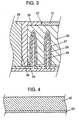
FIG. 3 is a cross sectional magnified view of an SEC, showing the key
portion in the first embodiment.
FIG. 4 is a cross sectional view of aluminum foil of an SEC, showing a
state after a resist film was formed in the first embodiment.
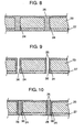
FIG. 5 is a cross sectional view of aluminum foil of an SEC, showing a
state after a first through hole was formed in the first embodiment.
FIG. 6 is a cross sectional view of aluminum foil of an SEC, showing a
state after an insulation film was formed in the first embodiment.
FIG. 7 is a cross sectional view of aluminum foil of an SEC, showing a
state after the resist film was removed in the first embodiment.
FIG. 8 is a cross sectional view of aluminum foil of an SEC, showing a
state after a dielectric layer was formed on the roughened surface in the first
embodiment.
FIG. 9 is a cross sectional view of aluminum foil of an SEC, showing a
state after a second through hole was formed in the first embodiment.
FIG. 10 is a cross sectional view of an SEC, showing a state after the
second through hole was filled with a conductive substance in the first
embodiment.
FIG. 11 is a cross sectional view of an SEC, showing a state after a
solid electrolytic layer was formed on the dielectric layer in the first
embodiment.
FIG. 12 is a cross sectional view of an SEC, showing a state after a
collector layer was formed in the first embodiment.
FIG. 13 is a cross sectional view of an SEC showing a state after an
opening was formed in the first embodiment.
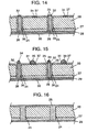
FIG. 14 is a cross sectional view of an SEC, showing a state after a
first connection terminal was formed in the first embodiment.
FIG. 15 is a cross sectional view of an SEC, showing a state after a
connection bump was formed in the first embodiment.
FIG. 16 is a cross sectional view of an SEC, showing a state after a
solid electrolytic layer was formed on a dielectric layer in a second exemplary
embodiment.
FIG. 17 is a cross sectional view of aluminum foil of an SEC, showing a
state after a second through hole was formed in the second embodiment.
FIG. 18 is a cross sectional view of an SEC, showing a state after a
second through hole was filled with a conductive substance in the second
embodiment.
FIG. 19 is a cross sectional view of an SEC, showing a state after a
collector layer was formed in the second embodiment.
FIG. 20 is a cross sectional view of an SEC, showing a state after an
opening was formed in the second embodiment.
FIG. 21 is a cross sectional view of an SEC, showing a state after a
first connection terminal was formed in the second embodiment.
BEST MODE FOR CARRYING OUT THE INVENTION
Method for manufacturing solid electrolytic capacitor (SEC) is
described in accordance with exemplary embodiments of the present invention,
referring to the drawings. The drawings are aimed to present the concepts,
not to exhibit precise dimensions.
(Embodiment 1)
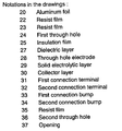
Referring to FIG. 2 and FIG. 3, an aluminum foil 20 has been
roughened in one of the surfaces, and a dielectric layer 27 is formed on the
roughened surface of the aluminum foil 20. Further on the surface of
dielectric layer 27, a solid electrolytic layer 29, which is substantially an
electrode, is provided to be functioning as a capacitor in combination with the
aluminum foil 20. The surface roughening of aluminum foil 20 is aimed to
expand the surface area of electrode portion, thereby increasing the static
capacitance of an SEC.
Provided on the surface of the solid electrolytic layer 29 is a collector
layer 30 for facilitating an easy lead-out of the electrode. The collector layer
30 is connected to a second connection terminal 32 via through hole electrode
28. The through hole electrode 28 is formed by filling a second through hole
36 with a conductive substance, which electrode is electrically insulated by an
insulation film 25 from the aluminum foil 20.
A first connection terminal 31 is connected direct with the aluminum
foil 20, while electrically insulated from the second connection terminal 32 by
insulation film 25. The connection terminals 31 and 32 are provided
respectively with connection bumps 33 and 34 for the purpose of direct
connection with a semiconductor component.
Thus the first connection terminal 31 and the second connection
terminal 32 are disposed on a same plane; which configuration makes it
possible to connect a semiconductor component direct with an SEC. Thereby,
the connecting distance between the components is remarkably shortened to a
reduced ESR and ESL.
Furthermore, by disposing the connection terminals in an
arrangement as shown in FIG. 1, directions of the electric current are
reversed among each other; thereby, the generated magnetic fields mutually
cancel to a reduced ESL.
FIGs. 4 through 15 show cross sectional views used to describe
manufacturing process of an SEC.
Referring to FIG. 4, a resist film 23 is formed on one of the surfaces of
aluminum foil 20. A photo sensitive resin or an adhesive organic film may be
used for the resist film 23. The film may be formed easily through such
methods as an immersion, a spin coating, a screen printing, a film attaching, a
spraying. Whichever method of the above can readily provide a resist film 23
on one surface at a high productivity.
A photo sensitive resin is advantageous in that it is easy to apply and
cure; while an organic film is advantageous in that it contributes to make the
manufacturing process simple, in addition, it can be peeled off easily at a later
process step. In the next step, the aluminum foil 20 is provided with a first
through hole 24, as shown in FIG. 5.
The first through hole 24 can be formed at any optional location with a
high precision by using at least one of the methods among a laser beam
machining, a punching method, a drilling method and an electric discharge
machining.
Next, as shown in FIG. 6, an insulation film 25 is formed on the
aluminum foil 20 covering the surface opposite to the one having the resist
film 23 and filling the first through hole. The material for insulation film 25
may be selected preferably among the group of an epoxy resin, a polyimide
resin, a silicone resin, an acrylic resin and a phenol resin. These materials
are superior in the insulating property, resistance against solvent and heat
withstanding property. Furthermore, they stick fast to the aluminum foil 20,
or the electrode. They not only protect the surface of aluminum foil 20 from
solvent, acid, etc. used during the manufacturing process, but they also play
the role of protecting an SEC from outside environments. The insulation
film 25 may be formed by using at least one of the methods among an
immersion, a spin coating, a screen printing, a spraying and an
electrodeposition. Whichever method can readily provide an insulation film
25 evenly on the surface of aluminum foil 20. Prior to formation of the
insulation film 25, the first through hole 24 of aluminum foil 20 may be
chamfered around the edge. The chamfering is aimed to get rid of burr that
might have emerged during formation of the first through hole 24, at the same
time it improves the covering property of insulation film 25 at the other
surface of aluminum foil 20, as a result it is effective to prevent possible
short-circuiting between the through hole electrode 28 and the aluminum foil
20. While on the one surface of the aluminum foil 20, it improves the
covering property of dielectric layer 27, which is effective to present possible
short-circuiting between the solid electrolytic layer 29 and the aluminum foil
20. As the result of above-described effects, an SEC is provided with stable
characteristics and the reliability is improved.
Next, as shown in FIG. 7, the resist film 23 sticking on one of the
surfaces of aluminum foil 20 is removed by, for example, immersing it in a
resist remover solution.
Then, as shown in FIG. 8, the surface of aluminum foil 20 is
roughened by etching in a region where the resist film 23 used to be and
removed, and a dielectric layer 27 is formed on the roughened surface of
aluminum foil 20. The surface-roughening etching may be conducted by, for
example, immersing it an acidic solution and applying a certain specific
voltage thereto, or simply immersing it in an acidic solution. The formation
of dielectric layer may be conducted by, for example, an anodic oxidation of the
aluminum foil 20 in an aqueous solution of ammonium adipate or an aqueous
solution of a mixture of boric acid and borax. FIG. 9 shows a state where a
second through hole 36 was formed in the insulation film 25 so that the
insulation film 25, which layer is filling the first through hole 24, is kept
staying around the wall surface of first through hole 24. The second through
hole 36 can be formed at a high accuracy within the insulation film filling the
first through hole, by using either one of the methods among a laser beam
machining, a punching and a drilling. Then, a through hole electrode 28 is
formed by filling the second through hole 36 with a conductive adhesive
substance and curing it, as shown in FIG. 10. This way of manufacturing can
provide a through hole electrode 28 easily. Then, a solid electrolytic layer 29
is formed on the surface of dielectric layer 27, as shown in FIG. 11.
The solid electrolytic layer 29 is formed by using at least one among
the group of a conductive polymer generated through a chemical
polymerization of heterocyclic monomer such as pyrrol, thiophene using an
oxidizing agent such as ferric sulfate, or through an electrolytic
polymerization where the aluminum foil 20 is immersed in a heterocyclic
monomer solution and applied with a voltage therein; manganese dioxide
generated by heat-decomposing manganese nitrate; a coated film formed by
applying a suspension of powdered conductive polymer; and a coated film
formed by applying an aqueous solution of conductive polymer.
The conductive polymer which has been made available through one of
the above processes may be formed on the surface of dielectric layer 27 after
the layer is provided with manganese dioxide on the surface.
The above process provides the conductive polymer homogeneously
and intensely. By using the above-described material and procedure, solid
electrolytic layer 29 can be provided even on the surface of dielectric layer 27
that has been formed in the micro etching pits generated as a result of the
roughening operation. Thus it contributes to a higher static capacitance of
an SEC.
Furthermore, in a case where the solid electrolytic layer 29 is formed
using an organic material, the layer is soft and flexible and can withstand
possible damage or breakage that might arise during the manufacturing
process. FIG. 12 shows a state after a collector layer 30 was formed on the
surface of solid electrolytic layer 29. The collector layer 30 is formed by
applying at least either one among the group of a suspension of carbon
particle, a conductive adhesive substance and a conductive paint. This
process improves the adhesive property between the solid electrolytic layer 29,
or a substantial electrode, and the collector layer 30, or an apparent electrode;
thereby, the ESR is reduced and the high frequency characteristic is improved.
FIG. 13 shows a state where an opening 37 was formed in the insulation film
using a laser beam machining or a grinding method, for providing a first
connection terminal 31 on the other surface of aluminum foil 20.
These methods can form the opening efficiently; which contributes to a
higher productivity. FIG. 14 shows a state where a first connection terminal
31 was provided in the opening 37.
The first connection terminal 31 is provided for facilitating a good
contact with other component, and is connected with the aluminum foil 20.
Preferred process of forming the first connection terminal 31 includes
application of conductive adhesive, electroplating, electroless plating.
The application of a conductive adhesive is advantageous in increasing
the manufacturing productivity, because of its easiness of application and
curing. In the case of electroplating and electroless plating, since it is
already covered with the insulation film 25 except the opening 37 and the
exposed portion of through hole electrode 28, the first connection terminals 31
can be provided altogether evenly with ease by covering the exposed surface of
through hole electrode 28 and the whole reverse surface of collector layer 30
with an insulation tape or the like item. Depending on the needs of insuring
a better connection with semiconductor component, a second connection
terminal 32 may be provided on the exposed surface of through hole electrode
28 by electroplating, electroless plating or other process. When forming the
second connection terminal 32, the first connection terminals 31 and the
second connection terminals 32 can be formed altogether by simply covering
the entire reverse surface of collector layer 30 with the above-described
insulation tape or the like item. FIG. 15 shows a state where a first
connection bump 33 and a second connection bump 34, which are made of at
least one among the group of solder, gold, tin and silver, were provided on the
first connection terminal 31 and the second connection terminal 32,
respectively, which were illustrated in FIG. 14. A second connection bump
may be formed direct, eliminating the second connection terminal 32.
Since the connection terminals are disposed on a same plane, it can be
connected direct with a semiconductor component. Thus the above-described
method of manufacture readily implements a low ESR and a low ESL, and
offers an SEC of superior high frequency characteristics.
(Embodiment 2)
FIG. 16 shows a state where a solid electrolytic layer 29 was formed on
the surface of dielectric layer 27, which had been formed on the roughened
surface of aluminum foil 20 as illustrated in FIG. 8 in the embodiment 1.
The solid electrolytic layer 29 is formed through the same process as
in the embodiment 1. The point of difference from the embodiment 1 is that
in the present embodiment 2 no through hole electrode 28 is yet provided at
the present stage; this arrangement has the following advantage. Since the
through hole electrode 28 is formed of a conductive adhesive substance, it can
be ill-affected by solvent, etc. used for forming the solid electrolytic layer 29;
viz. the through hole electrode might get swollen, eroded, or flaked off.
So, a range of selecting materials for the conductive adhesive
substance would eventually be limited.
However, in the manufacturing method in accordance with the present
embodiment 2 where the solid electrolytic layer 29 is provided first and then a
through hole electrode 28 is formed, the above-described influence by solvent,
etc. does not need to be taken into account. Therefore, the conductive
adhesive substance can be selected from among a wider range of candidate
materials. Then, as shown in FIG. 17, a second through hole 36 is formed by
a laser beam machining, a punching method, a drilling method, or an electric
discharge machining, etc. The second through hole 36 is filled with a
conductive adhesive substance, as shown in FIG. 18, and then it is cured to
provide a through hole electrode 28.
FIG. 19 shows a state where a collector layer 30 was formed on the
surface of solid electrolytic layer 29. The point of difference from that of the
embodiment 1 shown in FIG. 12 is that while the through hole electrode 28 in
FIG. 12 is connected with solid electrolytic layer 29, the through hole electrode
28 in FIG. 19 is connected also to the collector layer 30 besides the solid
electrolytic layer 29.
Thus the ESR is further reduced, and the high frequency
characteristic is improved. And then, an opening 37 is formed as shown in
FIGs. 20 and 21 by the same process as in the embodiment 1, and a first
connection terminal 31 is provided in the opening 37 to obtain an SEC.
A feature point of the manufacturing method in accordance with the
present invention is that it uses an aluminum foil before etching as the
starting material. It has following advantages: After the first through hole
24 having been formed in the aluminum foil 20, in a step for removing the
resist film 23 which is staying on one surface of the aluminum foil, an acidic
solution or an alkaline solution may be used, besides organic solvent, as the
resist remover in the present method of manufacture. If an acidic solution or
an alkaline solution is used for removing the resist film 23 in a case where an
aluminum foil 20 already having a roughened surface is employed as the
starting material, the solution may dissolve also the roughened surface of
aluminum foil 20, besides the resist film 23 staying on one surface. The
dissolved surface of aluminum foil may lead to a deteriorated static
capacitance of an SEC.
In the manufacturing method of the present invention, however, the
etching is applied after the resist film 23 formed on one surface of aluminum
foil 20 is removed. So, there can be no such worry as described in the above,
and a resist remover can be selected from among a wider range of candidate
materials.
Furthermore, in a case where the manufacturing is conducted in
accordance with the present embodiment 2, a conductive adhesive substance
may be selected from among a wider range of candidate materials.
Thus the present invention offers a wide range of freedom in the
process designing, making the manufacturing of SEC easy. The SEC
manufactured in accordance with the present invention provides following
advantages: Since the first connection terminal and the second connection
terminal are disposed on a same plane, it can be connected direct with a
semiconductor component as the source of power supply, and it has a superior
high frequency characteristic either.
Furthermore, since the dielectric substance formed of an organic
material is rich in flexibility, it can be mounted even on a circuit or a substrate
which is exposed to a bending stress. The mounting on such a circuit or a
substrate was substantially impossible. Still further, it can be buried in such
a substrate with ease. Thus the SECs make a certain contribution to
downsizing of apparatus.
INDUSTRIAL APPLICABILITY
As described in the above, the present invention offers a wide range of
freedom in designing the process. Consequently, the SECs can be
manufactured with ease at a high precision level. At the same time, the
manufacturing method of the present invention implements a high
productivity in the manufacturing operation. Thus it provides a certain
value in the industry.