Technical Field
The present invention relates to a heat-resistant resin
film with a metal layer used for manufacturing a flexible
wiring board, and a wiring board using the heat-resistant
resin film with the metal layer.
Background Art
Heat-resistant resin films are conventionally used in
various fields by making use of properties peculiar to
resins. For example, a FPC (Flexible Printed Circuit Board),
a TAB (Tape Automated Bonding) film carrier tape, and the
like are generally known. Each of these materials is
obtained by bonding a heat-resistant resin film of polyimide,
or the like, to a metal foil with an adhesive of an epoxy
resin, acrylic resin, polyamide resin, or NBR
(acrylonitrile-butadiene) type, or the like. At present,
the properties of the FPC and the film carrier tape depend
upon the performance of the adhesive used, and the excellent
heat resistance and other properties possessed by the heat-resistant
resin film are not sufficiently utilized. Even
when a polyimide film is used, the FPC and film carrier tape
generally have a soldering heat resistance of 300°C or less
in spite of the heat resistance of polyimide of 350°C or
more.
A known method for solving this problem comprises
coating an organic polar solvent solution of a polyimide
precursor or polyimide directly on a surface of a metal foil
without using an adhesive, removing the solvent, and then
imidizing the coating. However, this method does not use
the adhesive, and thus causes insufficient adhesion between
the metal foil and the polyimide, thereby causing the
problem of separating a wiring layer from the polyimide when
the metal layer is formed in a wiring pattern. Particularly,
when fine wiring with a pitch of 50 µm or less is formed,
adhesion is absolutely insufficient.
Also, a method of forming a metal thin layer on an
epoxy resin, acrylic resin, polyamide resin, or NBR adhesive
by a sputtering or wet process, and then further forming a
metal layer by plating is known. However, the adhesive has
no heat resistance, and thus the soldering heat resistance
is 300°C or less.
Disclosure of Invention
An object of the present invention is to solve the
problem of insufficient heat resistance and adhesion, and
provide a heat-resistant resin film with a metal layer,
which has high heat resistance and high adhesion, and a
wiring board obtained by patterning the heat-resistant resin
film with the metal layer in a wiring pattern.
The present invention provides a heat-resistant resin
film with a metal layer, comprising a heat-resistant
adhesive comprising a polyimide resin coated on the heat-resistant
resin film, and at least one metal layer provided
on the adhesive by sputtering, vacuum evaporation or plating.
Also, the present invention provides a wiring board obtained
by patterning the heat-resistant resin film with the metal
layer in a wiring pattern, and methods of producing the
heat-resistant resin film and the wiring board. In the
present invention, the heat-resistant adhesive comprising
the polyimide resin is combined with at least one metal
layer provided by sputtering, vacuum evaporation or plating,
thereby exhibiting high heat resistance and high adhesion.
Best Mode for Carrying Out the Invention
A heat-resistant resin film with a metal layer of the
present invention comprises a heat-resistant adhesive coated
on the heat-resistant resin film, and the metal layer formed
on the adhesive.
The heat-resistant resin film may be a polymeric resin
film satisfying either a melting point of 280°C or more, or
a maximum allowable temperature of 121°C or more in
continuous use for a long period of time defined by JIS
C4003.
Preferred examples of the polymeric resin film include
films of polyarylate, which is a condensation product of
bisphenol and a dicarboxylic acid, polyallylsulfone such as
polyethersulfone or polysulfone, a condensation product of
benzotetracarboxylic acid and aromatic isocyanate,
thermosetting polyimide obtained by reaction of bisphenol,
aromatic diamine and nitrophthalic acid, aromatic polyimide,
aromatic polyamide, aromatic polyetheramide,
polyphenylenesulfide, polyallylether ketone, polyamide-imide
resins, aramid resins, polyethylene naphthalate resins,
polyether ether ketone resins, and the like; liquid crystal
polymer films; and the like. Particularly, aromatic
polyimide films and liquid crystal polymer films are
preferably used. Examples of commercial products include
"Kapton" produced by Du Pont-Toray Co., Ltd., "Upilex"
produced by Ube Industries, Ltd., "Apical" produced by
Kaneka Corporation, "Mictron" produced by Toray Industries,
Inc., "Vectran" produced by Kuraray Co., Ltd., and the like.
Both or one of the surfaces of the heat-resistant resin
film is preferably treated by discharge treatment such as
corona discharge, atmospheric-pressure plasma treatment,
low-temperature plasma treatment, or the like for improving
adhesion. Examples of discharge treatment include discharge
under near atmospheric pressure, i.e., atmospheric-pressure
plasma treatment, corona discharge treatment, low-temperature
plasma treatment, and the like. By performing
the discharge treatment, adhesion can be improved.
The atmospheric-pressure plasma treatment means a
method of discharge treatment in an atmosphere of a
treatment gas such as argon, nitrogen, helium, carbon
dioxide, carbon monoxide, air, water vapor, or the like.
Although the treatment conditions depend upon the treatment
apparatus used, the type of the treatment gas used, the flow
rate, and the frequency of a power supply, the optimum
conditions can be appropriately selected.
The low-temperature plasma treatment can be performed
under low pressure, and the method is not limited. An
example of the method is a method in which a substrate to be
treated is set in an internal electrode-type discharge
apparatus comprising a counter electrode comprising a drum
electrode and a plurality of rod electrodes, a DC or AC high
voltage is applied between the electrodes for discharge with
a treatment gas adjusted to 0.01 to 10 Torr, preferably 0.02
to 1 Torr, to produce plasma of the treatment gas, and the
surface of the substrate is exposed to the plasma. Although
the conditions of the low-temperature plasma treatment
depend upon the treatment apparatus used, the type of the
treatment gas used, pressure, the frequency of a power
supply, etc., the optimum conditions can be appropriately
selected. The treatment gas is not limited, and argon,
nitrogen, helium, carbon dioxide, carbon monoxide, air,
water vapor, oxygen, carbon tetrafluoride, and the like can
be used singly or in a mixture.
On the other hand, the corona discharge treatment
exhibits a smaller adhesion improving effect than the low-temperature
plasma treatment, and it is thus important to
select the laminated heat-resistant adhesive.
The heat-resistant resin film preferably has a
thickness of 5 to 250 µm, and more preferably 10 to 80 µm.
An excessively thin film causes a defect in transfer, and an
excessively thick film causes a difficulty in forming a
through hole. Therefore, the thickness is preferably in the
above range.
In the present invention, as the heat-resistant
adhesive, a polyimide resin is individually used, or mixed
with another resin. Examples of the resin mixed include
epoxy resins, urethane resins, polyamide resins,
polyetherimide resins, polyamide-imide resins, and the like.
Alternatively at least two types of polyimide resins may be
mixed. The adhesive may contain organic or inorganic fine
particles, a filler, or the like, and a nucleating agent
described below. Particularly, from the viewpoint of heat
resistance, polyimide resins composed of an aromatic
tetracarboxylic acid and a diamine component are preferably
used. More preferably, polyimide resins each obtained by
imidizing a polyamic acid obtained by reaction of an
aromatic tetracarboxylic acid and 40 mol% or more of
siloxane-type diamine are used.
In the present invention, the heat-resistant adhesive
preferably has a glass transition temperature (Tg) of 60°C
to 250°C, and more preferably a glass transition temperature
of 60°C to 230°C. With a glass transition temperature of
less than 60°C, heat resistance deteriorates to cause a
defect in a high-temperature process using a lead-free
solder. With a glass transition temperature of over 250°C,
adhesion to the metal layer provided on the heat-resistant
adhesive undesirably deteriorates.
In the present invention, the heat-resistant adhesive
preferably has an elastic modulus of 0.1 GPa to 3.0 GPa at
200°C, and more preferably 0.3 GPa to 2.0 GPa at 200°C.
With an elastic modulus of less than 0.1 GPa at 200°C, heat
resistance undesirably deteriorates. With an elastic
modulus of over 3.0 GPa at 200°C, adhesion to the metal
layer provided on the heat-resistant adhesive undesirably
deteriorates.
Furthermore, in the present invention, the amount of
the gases generated from the heat-resistant adhesive at a
heating temperature of 100°C to 300°C is preferably 250 ppm
or less, more preferably 150 ppm or less, and most
preferably 100 ppm or less. The amount of the gases
generated at a heating temperature of 100°C to 300°C is
measured by thermogravimetry, micro decomposition and
gravimetry, or mass spectrometry. For example, the
temperature is increased from room temperature at 5°C/min to
measure the amount of the gases generated at 100°C to 300°C
by mass spectrometry using TG-MAS. In order to keep down
the amount of the gases generated, it is important that the
adhesive does not contain a low-boiling-point compound as a
component, does not have a site which is easily decomposed,
and has a structure which less absorbs water and carbon
dioxide gas. By using the heat-resistant adhesive
generating a suppressed amount of gases, peeling of the
metal layer due to the gases is eliminated to maintain high
adhesion.
In addition, the heat-resistant adhesive is preferably
as thin as possible to a degree causing no deterioration in
adhesion. With an excessively thick adhesive, not only the
properties of the heat-resistant resin film deteriorate, but
also the inside of the adhesive layer deteriorates to
adversely affect the heat resistance of the entire metal
layer with resin. Therefore, the thickness of the adhesive
is 0.01 µm to 10 µm, preferably 0.01 µm to 5 µm, and more
preferably 0.01 µm to 3 µm. With a thickness of less than
0.01 µm, adhesion undesirably deteriorates.
Examples of aromatic tetracarboxylic acid used for a
polyimide resin for obtaining the heat-resistant adhesive
having the above-described properties include 3,3',4,4'-benzophenone
tetracarboxylic dianhydride, 2,2',3,3'-benzophenone
tetracarboxylic dianhydride, 2,2',3,3'-biphenyl
tetracarboxylic dianhydride, pyromellitic dianhydride,
3,3',4,4'-biphenyl tetracarboxylic dianhydride, 2,2',3,3'-biphenyl
tetracarboxylic dianhydride, 2,2-bis(3,4-dicarboxyphenyl)propane
dianhydride, 2,2-bis(2,3-dicarboxyphenol)propane
dianhydride, bis(3,4-dicarboxyphenyl)
ether dianhydride, bis(3,4-dicarboxyphenyl)sulfone
dianhydride, 1,1-bis(2,3-dicarboxyphenyl)ethane
dianhydride, bis(2,3-dicarboxyphenyl)methane
dianhydride, 2,3,6,7-naphthalenetetracarboxylic
dianhydride, 1,4,5,8-naphthalenetetracarboxylic
dianhydride, 1,2,5,6-naphthalenetetracarboxylic
dianhydride, 1,2,3,4-benzenetetracarboxylic
dianhydride, 3,4,9,10-perylenetetracarboxylic
dianhydride, 2,3,6,7-anthracenetetracarboxylic
dianhydride, 1,2,7,8-phenanthrenetetracarboxylic
dianhydride, and the like.
These carboxylic acids are used individually or in a mixture
of at least two compounds,
A diamine used for a polyimide resin for obtaining the
heat-resistant adhesive having the above properties is
preferably at least 30 mol% or more of, more preferably 40
mol% or more of, siloxane-type diamine. The siloxane-type
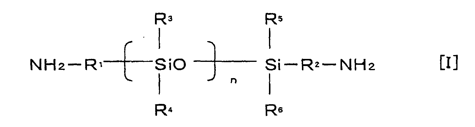
diamine used in the present invention is represented by the
following formula [1]:
(wherein n represents an integer of 1 or more, R1 and R2 may
be the same or different and each represent a lower alkylene
group or a phenylene group, and R3, R4, R5 and R6 may be the
same or different and each represent a lower alkyl group, a
phenylene group, or a phenoxy group.)
Examples of siloxane-type diamines represented by
formula [1] include 1,1,3,3-tetramethyl-1,3-bis(4-aminophenyl)
disiloxane, 1,1,3,3-tetraphenoxy-1,3-bis(4-aminoethyl)
disiloxane, 1,1,3,3,5,5-hexamethyl-1,5-bis(4-aminophenyl)
trisiloxane, 1,1,3,3-tetraphenyl-1,3-(2-aminoethyl)
disiloxane, 1,1,3,3-tetraphenyl-1,3-bis(3-aminopropyl)
disiloxane, 1,1,5,5-tetraphenyl-3,3-dimethyl-1,5-bis(3-aminopropyl)
trisiloxane, 1,1,5,5-tetraphenyl-3,3-dimethoxy-1,5-bis(4-aminobutyl)
trisiloxane, 1,1,5,5-tetraphenyl-3,3-dimethoxy-1,5-bis(5-aminophentyl)
trisiloxane, 1,1,3,3-tetramethyl-1,3-bis(2-aminoethyl)
disiloxane, 1,1,3,3-tetramethyl-1,3-bis(3-aminopropyl)
disiloxane, 1,1,3,3-tetramethyl-1,3-bis(4-aminobutyl)
disiloxane, 1,3-dimethyl-1,3-dimethoxy-1,3-bis(4-aminobutyl)
disiloxane, 1,1,5,5-tetramethyl-3,3-dimethoxy-1,5-bis(2-aminoethyl)
trisiloxane, 1,1,5,5-tetramethyl-3,3-dimethoxy-1,5-bis(4-aminobutyl)
trisiloxane, 1,1,5,5-tetramethyl-3,3-dimethoxy-1,5-bis(5-aminopentyl)
trisiloxane, 1,1,3,3,5,5-hexamethyl-1,5-bis(3-aminopropyl)
trisiloxane, 1,1,3,3,5,5-hexapropyl-1,5-bis(3-aminopropyl)
trisiloxane, and the like.
These siloxane-type diamines are used individually or in a
mixture of at least two compounds.
As a diamine component other than the siloxane-type
diamine, 4,4'-diaminodiphenyl ether, 4,4'-diaminodiphenyl
methane, 4,4'-diaminodiphenyl sulfone, paraphenylenediamine,
or the like can be used.
The method of obtaining polyamic acid as a polyimide
precursor by reaction of an aromatic tetracarboxylic acid
and diamine can be performed according to a conventional
known method. For example, substantially stoichiometric
amounts of acid component and diamine component may be
reacted at a temperature of 0 to 80°C in an organic solvent
such as N,N-dimethylformamide, N,N-dimethylacetamide, N-methyl-2-pyrrolidone,
or the like. These solvents are used
individually or in a mixture of at least two solvents, and
benzene, toluene, hexane, cyclohexane, tetrahydrofuran,
methyl ethyl ketone, or the like may be added to the solvent
to an extent causing no precipitation of polyamic acid. The
concentration of polyamic acid varnish is not limited, but
the concentration is preferably 5 to 60% by weight, and more
preferably 10 to 40% by weight. The resultant polyamic acid
varnish is coated on the heat-resistant resin film, dried,
and then imidized to form the heat-resistant adhesive
comprising the polyimide resin on the heat-resistant resin
film.
In the present invention, the metal layer is formed on
the heat-resistant adhesive. As the method of forming the
metal layer, a sputtering method, a vacuum evaporation
method, a plating method, or a combination thereof may be
used. Unlike in a method of bonding a copper foil, the
method of forming the metal layer by sputtering, vacuum
evaporation or plating forms a mixed layer containing the
heat-resistant adhesive and the metal layer at the interface
therebetween, thereby significantly improving adhesion
between both layers. Once the mixed layer is formed,
adhesive strength is maintained after the metal layer is
patterned to form a wiring pattern, and thus the mixed layer
is advantageous in forming fine wiring. Although copper,
nickel, chromium, tin, zinc, lead, gold, rhodium, palladium,
or the like can be used as a metal for forming the metal
layer, the metal is not limited to these metals. These
metals may be used individually or in a combination of at
least two metals.
When the metal layer is formed by sputtering or vacuum
evaporation, the metal is deposited to a proper thickness on
the heat-resistant adhesive by sputtering or vacuum
evaporation. As the sputtering or vacuum evaporation method,
a known method may be used.
When the metal layer is formed by plating, plating is
not performed directly on the adhesive, but plating is
generally performed after a metal thin film serving as a
nucleus is formed on the surface of the heat-resistant
adhesive. The method of forming the metal thin film as the
nucleus is divided into a wet process and a dry process.
The wet process is further divided into a case in which the
heat-resistant adhesive contains a catalytic nucleus, and a
case in which the heat-resistant adhesive does not contain a
catalytic nucleus. When the adhesive does not contain the
catalytic nucleus, palladium, tin, nickel, or chromium is
first applied as a catalyst to the surface of the heat-resistant
adhesive, and if required, the applied catalyst is
activated. When the adhesive contains the catalytic nucleus,
if required, the catalyst on the surface of the heat-resistant
adhesive is activated. In the dry process,
chromium, nickel, tin, copper, palladium, gold, aluminum, or
the like is deposited on the surface of the heat-resistant
adhesive by sputtering or vacuum evaporation. However, a
metal such as copper may be singly deposited by sputtering
or vacuum evaporation, or a combination of chromium-copper,
nickel-copper, or chromium-nickel may be deposited by
sputtering or vacuum evaporation. Although the thickness of
the metal thin film serving as the catalytic nucleus is not
limited, the thickness is preferably 1 nm to 1000 nm, and
more preferably 2 nm to 400 nm. With a thickness of over
1000 nm, much time is required for forming the metal thin
film, while with a thickness of less than 1 nm, a defect
occurs to damage plating, which will be described below.
Then, the metal layer is formed on the metal thin film
by plating. The metal layer may be formed only by
electroless plating, by a combination of electroless plating
and electroplating, or only by electroplating. The
electroless plating and electroplating can be performed by
known methods. For example, in the case of electroless
plating of copper, a combination of copper sulfate and
formaldehyde is used. In the case of electroplating of
copper, a copper sulfate plating solution, a copper cyanide
plating solution, or a copper pyrophosphate plating solution
may be used.
The thickness of the metal layer depends upon the way
of processing the heat-resistant resin film with the metal
layer. Namely, when a wiring board is formed by an additive
process (semi-additive or full-additive process) using the
heat-resistant resin film with the metal layer, a metal is
further laminated on the metal layer by plating. Therefore,
the thickness of the heat-resistant resin film with the
metal layer is preferably in the range of 0.1 µm to 18 µm,
and more preferably 0.1 µm to 10 µm. The thickness of less
than 0.1 µm is undesirable because a defect easily occurs.
The thickness of over 18 µm is also undesirable because much
time is required for removing an excessive portion of the
metal layer after the wiring board is formed by the additive
process, and the shape of the formed wiring impaired.
Conversely, when the wiring board is formed by a subtractive
process using the heat-resistant resin film with the metal
layer, a metal foil is used as wiring. Therefore, the
thickness of the heat-resistant resin film with the metal
layer is preferably in the range of 1 µm to 40 µm, and more
preferably 3 µm to 18 µm. The thickness of less than 1 µm
is undesirable because wiring is easily disconnected during
formation. The thickness of over 40 µm is also undesirable
because much time is required for forming wiring, and the
shape of the formed wiring is impaired.
The method of forming the heat-resistant resin film
with the metal layer comprises a series of steps, for
example, according to the following procedure. First, a
polyimide film as the heat-resistant resin film is treated
with low-temperature plasma. Next, the polyamic acid
varnish obtained as the polyimide resin heat-resistant
adhesive from the siloxane-type diamine is coated on the
polyimide film treated with low-temperature plasma. As the
coating method, a roll coater, a knife coater, a seal coater,
a comma coater, a doctor blade float coater, or the like can
be used. After coating, the coating is generally dried at a
temperature of 60°C to 200°C for 1 minute, and then imidized
at a temperature of 200°C to 350°C. The drying time is 1
minute to 60 minutes, and the imidizing time is 5 minutes to
30 minutes, but these times are not limited. Then, a
nickel-chromium alloy (nickel 90%-chromium 10% alloy) is
deposited on the heat-resistant adhesive by sputtering, and
then copper is deposited by sputtering. Finally,
electroplating copper is performed by using the sputtered
copper layer as an electrode to form the heat-resistant
resin film with the metal layer.
In the present invention, the heat-resistant adhesive
comprising the polyimide resin is formed on the heat-resistant
resin film, and then at least one metal layer is
formed on the adhesive by sputtering or vacuum evaporation.
By forming the heat-resistant adhesive comprising the
polyimide resin, strong adhesion can be obtained, as
compared with a case in which the metal layer is formed
directly on the heat-resistant resin film. Particularly,
when the metal layer is etched in a predetermined wiring
pattern, good adhesion can be obtained, causing an advantage
in forming fine wiring.
In the present invention, the adhesion is represented
by a value obtained by peeling a metal wiring pattern of 3
mm wide at a rate of 50 mm/min in the direction of 180
degrees according to JIS C5016 Section 7.1. The value is
preferably 5 N/cm or more, and more preferably 10 N/cm or
more. With the heat-resistant resin film with the metal
layer of the present invention, a value of 10 N/cm or more
can easily be obtained. Also, the heat-resistant adhesive
is every thin, and thus the adhesive has the advantage that
the properties basically possessed by the heat-resistant
resin film are not deteriorated.
The heat-resistant resin film with the metal layer of
the present invention is used for forming a wiring board by
the additive process or subtractive process. The
subtractive process comprises forming a resist layer on the
metal layer, patterning the resist layer into a shape
corresponding to a wiring pattern by exposure and
development, etching the metal layer through the patterned
resist layer used as a mask to form the wiring pattern, and
then removing the resist layer to obtain a wiring board.
The semi-additive process comprises forming a resist layer
on the metal layer, removing the resist layer, by exposure
and development, from a portion where a wiring pattern is
formed, forming the wiring pattern in the portion without
the resist layer by plating, removing the resist layer, and
then removing the metal layer from a portion other than the
wiring pattern to obtain a wiring board. Each of the thus-obtained
wiring boards comprises the heat-resistant resin
film and the metal wiring, which are strongly bonded
together with the heat-resistant adhesive provided
therebetween, and exhibits excellent heat resistance.
The heat-resistant resin film with the metal layer of
the present invention has the metal layer provided on both
or one of the sides of the heat-resistant resin film, and
thus wiring is formed on the heat-resistant resin film by
the additive or subtractive process to obtain a single-sided
or double-sided wiring board. Therefore, the heat-resistant
resin film can be preferably used for flexible wiring boards.
Examples
Although the present invention will be described with
reference to examples, the present invention is not limited
to these examples. In a description below, in Examples 1 to
15 and Comparative Examples 1 to 3, adhesion was evaluated
and measured by the following methods.
Example 1
112.5 g of N,N-dimethylacetamide was placed in a 300-ml
four-neck flask with a thermometer, a stirrer, a reflux
condenser, and a dry nitrogen gas inlet port, and 16.2 g (99
mol%) of 1,1,3,3-tetramethyl-1,3-bis(3-aminopropyl)
disiloxane and 0.07 g (1 mol%) of p-phenylenediamine were
dissolved under a nitrogen flow. Then, 21.22 g (100 mol%)
of 3,3',4,4'-benzophenonetetracarboxylic dianhydride was
added to the resultant solution, and then stirred at 10°C
for 1 hour. Then, the mixture was reacted by further
stirring at 50°C for 3 hours to obtain polyamic acid varnish.
The thus-obtained varnish was coated on one side of a
polyimide film ("Kapton" 100EN produced by Du Pont-Toray Co.,
Ltd.), which was a heat-resistant resin film of 25 µm
treated with low-temperature plasma in an argon atmosphere,
by a bar coater so that the thickness after drying was 3 µm.
Then, heat treatment was performed at 130°C for 3 minutes,
150°C for 3 minutes, and further 270°C for 3 minutes to dry
and imidize the coated film. As a result, a heat-resistant
adhesive comprising the polyimide resin was formed on one
side of the heat-resistant resin film. The glass transition
temperature (Tg) of the heat-resistant adhesive was 92°C,
the elastic modulus at 200°C was 0.4 GPa, and the amount of
the gases generated at 100 to 300°C was 90 ppm.
Then, chromium was deposited to a thickness of 4 nm on
the heat-resistant adhesive by sputtering, and copper was
deposited to a thickness of 200 nm by sputtering. After
sputtering, electrolytic copper plating was performed to a
thickness of 8 µm by using a copper sulfate bath with a
current density of 2 A/dm2 to obtain the heat-resistant
resin film with a metal layer.
Example 2
The varnish obtained in Example 1 was coated on one
side of a polyimide film of 25 µm thick ("Upilex" 25S
produced by Ube Industries, Ltd.) treated with plasma by the
same method as Example 1 so that the thickness after drying
was 0.5 µm, dried and then imidized by the same method as
Example 1 to form a heat-resistant adhesive comprising the
polyimide resin on the heat-resistant resin film. The glass
transition temperature (Tg) of the heat-resistant adhesive
was 92°C, the elastic modulus at 200°C was 0.4 GPa, and the
amount of the gases generated at 100 to 300°C was 90 ppm.
Then, nickel was deposited to a thickness of 10 nm on
the heat-resistant adhesive by sputtering, and copper was
deposited to a thickness of 100 nm by sputtering. After
sputtering, copper plating was performed to a thickness of 2
µm by the same method as Example 1 to obtain the heat-resistant
resin film with a metal layer.
Example 3
The varnish obtained in Example 1 was coated on one
side of a liquid crystal polymer film of 25 µm thick ("Biac"
produced by Japan Gore-Tex Inc.) treated with plasma by the
same method as Example 1 so that the thickness after drying
was 9 µm, dried and then imidized by the same method as
Example 1 to form a heat-resistant adhesive comprising the
polyimide resin on the heat-resistant resin film. The glass
transition temperature (Tg) of the heat-resistant adhesive
was 92°C, the elastic modulus at 200°C was 0.4 GPa, and the
amount of the gases generated at 100 to 300°C was 90 ppm.
Then, a nickel-chromium alloy (nickel 95%-chromium 5%)
was deposited to a thickness of 6 nm on the heat-resistant
adhesive by sputtering, and copper was deposited to a
thickness of 350 nm by sputtering. After sputtering, copper
plating was performed to a thickness of 15 µm by the same
method as Example 1 to obtain the heat-resistant resin film
with a metal layer.
Example 4
112.5 g of N,N-dimethylacetamide was placed in a 300-ml
four-neck flask with a thermometer, a stirrer, a reflux
condenser, and a dry nitrogen gas inlet port, and 6.94 g (40
mol%) of 1,1,3,3-tetramethyl-1,3-bis(3-aminopropyl)
disiloxane and 11.79 g (60 mol%) of diaminodiphenyl ether
were dissolved under a nitrogen flow. Then, 21.32 g (100
mol%) of 3,3',4,4'-benzophenonetetracarboxylic dianhydride
was added to the resultant solution, and then stirred at
10°C for 1 hour. Then, the mixture was reacted by further
stirring at 50°C for 3 hours to obtain polyamic acid varnish.
The thus-obtained varnish was coated on one side of a
polyimide film ("Kapton" 100EN produced by Du Pont-Toray Co.,
Ltd.), which was a heat-resistant resin film of 25 µm
treated with low-temperature plasma in an argon atmosphere,
by a bar coater so that the thickness after drying was 3 µm.
Then, heat treatment was performed at 130°C for 3 minutes,
150°C for 3 minutes, and further 270°C for 3 minutes to dry
and imidize the coated film. As a result, a heat-resistant
adhesive was formed on one side of the heat-resistant resin
film. The glass transition temperature (Tg) of the heat-resistant
adhesive was 175°C, the elastic modulus at 200°C
was 1.3 GPa, and the amount of the gases generated at 100 to
300°C was 60 ppm.
Then, chromium was deposited to a thickness of 4 nm on
the heat-resistant adhesive by sputtering, and copper was
deposited to a thickness of 200 nm by sputtering. After
sputtering, electrolytic copper plating was performed to a
thickness of 8 µm by using a copper sulfate bath with a
current density of 2 A/dm2 to obtain the heat-resistant
resin film with a metal layer.
Example 5
The varnish obtained in Example 4 was coated on one
side of a polyimide film of 25 µm thick ("Upilex" 25S
produced by Ube Industries, Ltd.) treated with plasma by the
same method as Example 4 so that the thickness after drying
was 0.5 µm, dried and then imidized by the same method as
Example 4 to form a heat-resistant adhesive on the heat-resistant
resin film. The glass transition temperature (Tg)
of the heat-resistant adhesive was 175°C, the elastic
modulus at 200°C was 1.3 GPa, and the amount of the gases
generated at 100 to 300°C was 60 ppm.
Then, nickel was deposited to a thickness of 10 nm on
the heat-resistant adhesive by sputtering, and copper was
deposited to a thickness of 100 nm by sputtering. After
sputtering, copper plating was performed to a thickness of 2
µm by the same method as Example 4 to obtain the heat-resistant
resin film with a metal layer.
Example 6
The varnish obtained in Example 4 was coated on one
side of a liquid crystal polymer film of 25 µm thick ("Biac"
produced by Japan Gore-Tex Inc.) treated with plasma by the
same method as Example 4 so that the thickness after drying
was 9 µm, dried and then imidized by the same method as
Example 4 to form a heat-resistant adhesive on the heat-resistant
resin film. The glass transition temperature (Tg)
of the heat-resistant adhesive was 175°C, the elastic
modulus at 200°C was 1.3 GPa, and the amount of the gases
generated at 100 to 300°C was 60 ppm.
Then, a nickel-chromium alloy (nickel 95%-chromium 5%)
was deposited to a thickness of 6 nm on the heat-resistant
adhesive by sputtering, and copper was deposited to a
thickness of 350 nm by sputtering. After sputtering, copper
plating was performed to a thickness of 15 µm by the same
method as Example 4 to obtain the heat-resistant resin film
with a metal layer.
Example 7
140 g of N,N-dimethylacetamide was placed in a 300-ml
four-neck flask with a thermometer, a stirrer, a reflux
condenser, and a dry nitrogen gas inlet port, and 10.2 g (65
mol%) of 1,1,3,3-tetramethyl-1,3-bis(3-aminopropyl)
disiloxane and 4.42 g (35 mol%) of diaminodiphenyl ether
were dissolved under a nitrogen flow. Then, 20.36 g (100
mol%) of 3,3',4,4'-benzophenonetetracarboxylic dianhydride
was added to the resultant solution, and then stirred at
10°C for 1 hour. Then, the mixture was reacted by further
stirring at 50°C for 3 hours to obtain polyamic acid varnish.
The thus-obtained varnish was coated on one side of a
polyimide film ("Kapton" 100EN produced by Du Pont-Toray Co.,
Ltd.), which was a heat-resistant resin film of 25 µm
treated with low-temperature plasma in an argon atmosphere,
by a bar coater so that the thickness after drying was 3 µm.
Then, heat treatment was performed at 130°C for 3 minutes,
150°C for 3 minutes, and further 270°C for 3 minutes to dry
and imidize the coated film. As a result, a heat-resistant
adhesive was formed on one side of the heat-resistant resin
film. The glass transition temperature (Tg) of the heat-resistant
adhesive was 160°C, the elastic modulus at 200°C
was 0.9 GPa, and the amount of the gases generated at 100 to
300°C was 70 ppm.
Then, chromium was deposited to a thickness of 4 nm on
the heat-resistant adhesive by sputtering, and copper was
deposited to a thickness of 200 nm by sputtering. After
sputtering, electrolytic copper plating was performed to a
thickness of 8 µm by using a copper sulfate bath with a
current density of 2 A/dm2 to obtain the heat-resistant
resin film with a metal layer.
Example 8
The varnish obtained in Example 7 was coated on one
side of a polyimide film of 25 µm thick ("Upilex" 25S
produced by Ube Industries, Ltd.) treated with plasma by the
same method as Example 7 so that the thickness after drying
was 0.5 µm, dried and then imidized by the same method as
Example 7 to form a heat-resistant adhesive on the heat-resistant
resin film. The glass transition temperature (Tg)
of the heat-resistant adhesive was 160°C, the elastic
modulus at 200°C was 0.9 GPa, and the amount of the gases
generated at 100 to 300°C was 70 ppm.
Then, nickel was deposited to a thickness of 10 nm on
the heat-resistant adhesive by sputtering, and copper was
deposited to a thickness of 100 nm by sputtering. After
sputtering, copper plating was performed to a thickness of 2
µm by the same method as Example 7 to obtain the heat-resistant
resin film with a metal layer.
Example 9
The varnish obtained in Example 7 was coated on one
side of a liquid crystal polymer film of 25 µm thick ("BIAC"
produced by Japan Gore-Tex Inc.) treated with plasma by the
same method as Example 7 so that the thickness after drying
was 9 µm, dried and then imidized by the same method as
Example 7 to form a heat-resistant adhesive on the heat-resistant
resin film. The glass transition temperature (Tg)
of the heat-resistant adhesive was 160°C, the elastic
modulus at 200°C was 0.9 GPa, and the amount of the gases
generated at 100 to 300°C was 70 ppm.
Then, a nickel-chromium alloy (nickel 95%-chromium 5%)
was deposited to a thickness of 6 nm on the heat-resistant
adhesive by sputtering, and copper was deposited to a
thickness of 350 nm by sputtering. After sputtering, copper
plating was performed to a thickness of 15 µm by the same
method as Example 7 to obtain the heat-resistant resin film
with a metal layer.
Example 10
140 g of N,N-dimethylacetamide was placed in a 300-ml
four-neck flask with a thermometer, a stirrer, a reflux
condenser, and a dry nitrogen gas inlet port, and 13.1 g (95
mol%) of 1,1,3,3-tetramethyl-1,3-bis(3-aminopropyl)
disiloxane and 1.86 g (15 mol%) of diaminodiphenyl ether
were dissolved under a nitrogen flow. Then, 20.01 g (100
mol%) of 3,3',4,4'-benzophenonetetracarboxylic dianhydride
was added to the resultant solution, and then stirred at
10°C for 1 hour. Then, the mixture was reacted by further
stirring at 50°C for 3 hours to obtain polyamic acid varnish.
The thus-obtained varnish was coated on one side of a
polyimide film ("Kapton" 100EN produced by Du Pont-Toray Co.,
Ltd.), which was a heat-resistant resin film of 25 µm
treated with low-temperature plasma in an argon atmosphere,
by a bar coater so that the thickness after drying was 3 µm.
Then, heat treatment was performed at 130°C for 3 minutes,
150°C for 3 minutes, and further 270°C for 3 minutes to dry
and imidize the coated film. As a result, a heat-resistant
adhesive was formed on one side of the heat-resistant resin
film. The glass transition temperature (Tg) of the heat-resistant
adhesive was 130°C, the elastic modulus at 200°C
was 0.62 GPa, and the amount of the gases generated at 100
to 300°C was 50 ppm.
Then, chromium was deposited to a thickness of 4 nm on
the heat-resistant adhesive by sputtering, and copper was
deposited to a thickness of 200 nm by sputtering. After
sputtering, electrolytic copper plating was performed to a
thickness of 8 µm by using a copper sulfate bath with a
current density of 2 A/dm2 to obtain the heat-resistant
resin film with a metal layer.
Example 11
The varnish obtained in Example 10 was coated on one
side of a polyimide film of 25 µm thick ("Upilex" 25S
produced by Ube Industries, Ltd.) treated with plasma by the
same method as Example 10 so that the thickness after drying
was 0.5 µm, dried and then imidized by the same method as
Example 10 to form a heat-resistant adhesive on the heat-resistant
resin film. The glass transition temperature (Tg)
of the heat-resistant adhesive was 130°C, the elastic
modulus at 200°C was 0.62 GPa, and the amount of the gases
generated at 100 to 300°C was 50 ppm.
Then, nickel was deposited to a thickness of 10 nm on
the heat-resistant adhesive by sputtering, and copper was
deposited to a thickness of 100 nm by sputtering. After
sputtering, copper plating was performed to a thickness of 2
µm by the same method as Example 10 to obtain the heat-resistant
resin film with a metal layer.
Example 12
The varnish obtained in Example 10 was coated on one
side of a liquid crystal polymer film of 25 µm thick ("Biac"
produced by Japan Gore-Tex Inc..) treated with plasma by the
same method as Example 10 so that the thickness after drying
was 9 µm, dried and then imidized by the same method as
Example 10 to form a heat-resistant adhesive on the heat-resistant
resin film. The glass transition temperature (Tg)
of the heat-resistant adhesive was 130°C, the elastic
modulus at 200°C was 0.62 GPa, and the amount of the gases
generated at 100 to 300°C was 50 ppm.
Then, a nickel-chromium alloy (nickel 95%-chromium 5%)
was deposited to a thickness of 6 nm on the heat-resistant
adhesive by sputtering, and copper was deposited to a
thickness of 350 nm by sputtering. After sputtering, copper
plating was performed to a thickness of 15 µm by the same
method as Example 10 to obtain the heat-resistant resin film
with a metal layer.
Example 13
The same procedure as Example 1 was repeated except
that chromium was deposited to a thickness of 4 nm by vacuum
evaporation instead of being deposited to a thickness of 4
nm by sputtering, to obtain a heat-resistant resin film with
a metal layer.
Example 14
The same procedure as Example 2 was repeated except
that nickel was deposited to a thickness of 10 nm by vacuum
evaporation instead of being deposited to a thickness of 10
nm by sputtering, to obtain a heat-resistant resin film with
a metal layer.
Example 15
The same procedure as Example 3 was repeated except
that a nickel-chromium alloy (nickel 95%-chromium 5%) was
deposited to a thickness of 6 nm by vacuum evaporation
instead of being deposited to a thickness of 6 nm by
sputtering, to obtain a heat-resistant resin film with a
metal layer.
Comparative Example 1
Chromium was deposited to a thickness of 4 nm on one
side of a polyimide film ("Kapton" 100EN produced by Du
Pont-Toray Co., Ltd.), which was a heat-resistant resin film
of 25 µm treated with low-temperature plasma in an argon
atmosphere, by sputtering in the same manner as Example 1,
and then copper was deposited to a thickness of 200 nm by
sputtering. After sputtering, electrolytic copper plating
was performed to a thickness of 8 µm by using a copper
sulfate bath with a current density of 2 A/dm2 to obtain the
heat-resistant resin film with a metal layer.
Comparative Example 2
Nickel was deposited to a thickness of 10 nm on one
side of a polyimide film of 25 µm thick ("Upilex" 25S
produced by Ube Industries, Ltd.) treated with low-temperature
plasma in an argon atmosphere, by sputtering in
the same manner as Example 2, and then copper was deposited
to a thickness of 100 nm by sputtering. After sputtering,
copper plating was performed to a thickness of 2 µm by the
same method as Example 2 to obtain a heat-resistant resin
film with a metal layer.
Comparative Example 3
A nickel-chromium alloy (nickel 95%-chromium 5%) was
deposited to a thickness of 6 nm on one side of a liquid
crystal polymer film of 25 µm thick ("BIAC" produced by
Japan Gore-Tex Inc..) treated with low-temperature plasma in
an argon atmosphere by sputtering in the same manner as
Example 3, and then copper was deposited to a thickness of
350 nm by sputtering. After sputtering, copper plating was
performed to a thickness of 15 µm by the same method as
Example 3 to obtain a heat-resistant resin film with a metal
layer.
Example 16
Photoresist was coated on the metal layer of the heat-resistant
resin film with the metal layer obtained in
Example 1 so that the dry film thickness was 5 µm, dried,
and then patterned by exposure and development through a
mask corresponding to a wiring pattern having a line width
of 5 to 100 µm, to obtain a resist pattern having the
remaining wiring layer pattern. Then, the metal layer in
the portion in which the resist was removed was etched with
a 10% iron chloride aqueous solution, and further etched
with a 20% potassium ferricyanide aqueous solution
containing 5% of sodium hydroxide. Then, the photoresist
was removed to obtain a single-sided wiring board. In the
thus-obtained wiring board, thin wiring of 5 µm in thickness,
and relatively thick wiring of 100 µm in thickness were
strongly bonded without a defect in the wiring pattern.
Example 17
Photoresist was coated on the metal layer of the heat-resistant
resin film with the metal layer obtained in
Example 2 so that the dry film thickness was 5 µm, dried,
and then patterned by exposure and development through a
mask corresponding to a wiring pattern having a line width
of 5 to 100 µm, to obtain a resist pattern in which the
wiring layer pattern was removed. Then, in the portion in
which the resist was removed, electroless copper plating was
performed to a thickness of 0.5 µm on the metal layer, and
electrolytic copper plating was performed to a thickness of
3.5 µm. Then, electrolytic nickel plating was performed to
a thickness of 0.5 µm, and then electrolytic gold plating
was performed to a thickness of 3.5 µm so that the final
thickness was 5 µm the same as the resist layer. After
plating, the resist was removed, and the metal layer was
removed from the portion other than the wiring pattern by
soft etching with a 5% iron chloride aqueous solution to
obtain a single-sided wiring board. In the thus obtained
wiring board, thin wiring of 5 µm in thickness, and
relatively thick wiring of 100 µm in thickness were strongly
bonded without a defect in the wiring pattern.
The results of Examples 1 to 15 and Comparative
Examples 1 to 3 are summarized in Table 1.
| | Adhesive Strength (N/cm) |
| | Initial | After heat load | After tinning |
| Example 1 | 10 | 9 | 9 |
| Example 2 | 10 | 9 | 9 |
| Example 3 | 10 | 9 | 9 |
| Example 4 | 10 | 9 | 9 |
| Example 5 | 10 | 9 | 9 |
| Example 6 | 10 | 9 | 9 |
| Example 7 | 8 | 7 | 7 |
| Example 8 | 8 | 8 | 8 |
| Example 9 | 8 | 8 | 8 |
| Example 10 | 9 | 8 | 9 |
| Example 11 | 9 | 9 | 9 |
| Example 12 | 9 | 8 | 9 |
| Example 13 | 8 | 7 | 7 |
| Example 14 | 8 | 7 | 7 |
| Example 15 | 8 | 7 | 7 |
| Comp. Example 1 | 4 | 1 | 2 |
| Comp. Example 2 | 2 | 1 | 1 |
| Comp. Example 3 | 2 | 1 | 1 |
In the present invention, a heat-resistant resin film
with a metal layer comprises a metal layer formed on the
heat-resistant resin film by sputtering, vacuum evaporation
or plating using a heat-resistant adhesive comprising a
polyimide resin. Therefore, the physical properties
possessed by the heat-resistant resin film can be
sufficiently utilized, and the metal layer is strongly
bonded to the heat-resistant resin film. A wiring board
obtained by using the heat-resistant resin film with the
metal layer has less defect in a wiring pattern, and the
like, and thus has excellent properties.