EP1406305A2 - Charge-coupled device (CCD) and method of operating the same - Google Patents
Charge-coupled device (CCD) and method of operating the same Download PDFInfo
- Publication number
- EP1406305A2 EP1406305A2 EP03077990A EP03077990A EP1406305A2 EP 1406305 A2 EP1406305 A2 EP 1406305A2 EP 03077990 A EP03077990 A EP 03077990A EP 03077990 A EP03077990 A EP 03077990A EP 1406305 A2 EP1406305 A2 EP 1406305A2
- Authority
- EP
- European Patent Office
- Prior art keywords
- charge
- conductivity type
- coupled device
- gates
- phases
- Prior art date
- Legal status (The legal status is an assumption and is not a legal conclusion. Google has not performed a legal analysis and makes no representation as to the accuracy of the status listed.)
- Granted
Links
- 238000000034 method Methods 0.000 title claims abstract description 8
- 238000009825 accumulation Methods 0.000 claims abstract description 14
- 239000000758 substrate Substances 0.000 claims abstract description 12
- 239000002800 charge carrier Substances 0.000 claims abstract description 8
- 230000008859 change Effects 0.000 claims abstract description 5
- 230000004888 barrier function Effects 0.000 claims abstract description 4
- 238000001444 catalytic combustion detection Methods 0.000 description 35
- 230000008901 benefit Effects 0.000 description 4
- 238000003384 imaging method Methods 0.000 description 4
- 238000010586 diagram Methods 0.000 description 3
- 239000002184 metal Substances 0.000 description 3
- 239000007943 implant Substances 0.000 description 2
- 230000007704 transition Effects 0.000 description 2
- 239000012535 impurity Substances 0.000 description 1
- 238000004519 manufacturing process Methods 0.000 description 1
- 238000005381 potential energy Methods 0.000 description 1
- 230000008569 process Effects 0.000 description 1
- 239000007787 solid Substances 0.000 description 1
Images


Classifications
-
- H—ELECTRICITY
- H04—ELECTRIC COMMUNICATION TECHNIQUE
- H04N—PICTORIAL COMMUNICATION, e.g. TELEVISION
- H04N25/00—Circuitry of solid-state image sensors [SSIS]; Control thereof
- H04N25/70—SSIS architectures; Circuits associated therewith
- H04N25/71—Charge-coupled device [CCD] sensors; Charge-transfer registers specially adapted for CCD sensors
- H04N25/713—Transfer or readout registers; Split readout registers or multiple readout registers
-
- H—ELECTRICITY
- H04—ELECTRIC COMMUNICATION TECHNIQUE
- H04N—PICTORIAL COMMUNICATION, e.g. TELEVISION
- H04N25/00—Circuitry of solid-state image sensors [SSIS]; Control thereof
- H04N25/60—Noise processing, e.g. detecting, correcting, reducing or removing noise
- H04N25/63—Noise processing, e.g. detecting, correcting, reducing or removing noise applied to dark current
-
- H—ELECTRICITY
- H10—SEMICONDUCTOR DEVICES; ELECTRIC SOLID-STATE DEVICES NOT OTHERWISE PROVIDED FOR
- H10D—INORGANIC ELECTRIC SEMICONDUCTOR DEVICES
- H10D44/00—Charge transfer devices
- H10D44/40—Charge-coupled devices [CCD]
- H10D44/45—Charge-coupled devices [CCD] having field effect produced by insulated gate electrodes
- H10D44/462—Buried-channel CCD
- H10D44/466—Three-phase CCD
-
- H—ELECTRICITY
- H10—SEMICONDUCTOR DEVICES; ELECTRIC SOLID-STATE DEVICES NOT OTHERWISE PROVIDED FOR
- H10D—INORGANIC ELECTRIC SEMICONDUCTOR DEVICES
- H10D44/00—Charge transfer devices
- H10D44/40—Charge-coupled devices [CCD]
- H10D44/45—Charge-coupled devices [CCD] having field effect produced by insulated gate electrodes
- H10D44/462—Buried-channel CCD
- H10D44/468—Four-phase CCD
-
- H—ELECTRICITY
- H10—SEMICONDUCTOR DEVICES; ELECTRIC SOLID-STATE DEVICES NOT OTHERWISE PROVIDED FOR
- H10F—INORGANIC SEMICONDUCTOR DEVICES SENSITIVE TO INFRARED RADIATION, LIGHT, ELECTROMAGNETIC RADIATION OF SHORTER WAVELENGTH OR CORPUSCULAR RADIATION
- H10F39/00—Integrated devices, or assemblies of multiple devices, comprising at least one element covered by group H10F30/00, e.g. radiation detectors comprising photodiode arrays
- H10F39/10—Integrated devices
- H10F39/12—Image sensors
- H10F39/15—Charge-coupled device [CCD] image sensors
- H10F39/152—One-dimensional array CCD image sensors
Definitions
- the invention relates generally to the field of charge-coupled devices and, more particularly, to such charge-coupled devices having substantially no capacitance when in the accumulation mode.
- prior art charge-coupled devices 10 typically include a substrate or well 20 of the first conductivity type and buried channel 30 of the second conductivity type for the transfer of charge packets 40.
- a plurality of gates 50 are separated from the buried channel 30 by a thin insulating layer 60.
- the first conductivity type is p-type and the second conductivity type is n-type.
- the charge packets 40 are electrons flowing in the n-type buried channel 30.
- the opposite type of the electron charge packets 40 will be holes flowing in the p-type substrate or well 20.
- Voltages applied to the gates 50 alter the potential energy within the buried channel 30 for the purpose of controlling the transfer of charge packets 40 through the charge-coupled device 10.
- Additional p-type implants 70 are used to selectively alter the channel potential under the gates 50 for controlling the direction of charge packet 40 transfer.
- the charge packets 40 transferred through the buried channel 30 were generated by photons.
- the photo-generated electrons in the charge packets 40 are called photoelectrons.
- the photoelectrons are generated directly in the CCD.
- the photoelectrons are generated in photodiodes adjacent to the CCD.
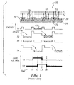
- Fig. 1 At time T1 all gate 50 voltages are at the low level which accumulates holes at the surface of the buried channel 30. At time T1, the thermal generation of dark current is lowest. To move the charge packets 40, the gates 50 must be clocked.
- the CCD shown in Fig. 1 is a two phase CCD. It has two sets of gates, the first set 51 is clocked at voltage V1 and the second set 52 is clocked at voltage V2. The clocking sequence of the voltages V1 and V2 are shown in Fig. 1. It is well understood that CCDs may be fabricated with more than two sets of gates.
- the gate 50 clocking scheme of U.S. Pat. 4,963,952 is sufficient for CCDs built in p-type substrates.
- the p-type substrate acts as a source or sink ofholes as the gates 50 are clocked between accumulation and depletion voltages.
- many interline CCD image sensors are built on n-type substrates 100 with p-type wells 20.
- the well 20 is confined in a narrow layer between the substrate 100 and buried channel 30. Now the well 20 can not easily act as a source or sink of holes.
- the holes must flow long distances from the well contact 110 at the perimeter of the CCD to the center of the CCD.
- the well 20 has a high resistance to the flow of holes.
- the nth gate 50 has a capacitance to the well 20 given by C n .
- the well 20 has a resistance from the well contact 110 to the nth gate given by R n .
- the invention resides in A method for reducing dark current within a charge coupled device comprising the steps of: (a) providing three or more phases of gates separated by an insulating layer from a buried channel of the first conductivity type in a well or substrate of the second conductivity type, and a clock driver for causing the transfer of charge through the charge coupled device; (b) providing a barrier for separating charge packets when in accumulation state; (c) applying, at a first time period, voltages to all phases of gates sufficient to cause the surface of the first conductivity type to be accumulated by dark current reducing charge carriers; after the first time period, applying, at each gate phase n having a capacitance C n to the layer of the second conductivity type, a voltage change on the gate phase n given by ⁇ V n such that the sum of products of the capacitances and voltage changes is substantially zero and after the voltage changes required to transfer charge through the
- the present invention has the advantage of reducing dark current, particularly in a three or more phase device, by enabling holes to flow more freely in accumulation without the need for additional contacts, which are undesirable as described hereinabove.
- the CCD 150 has four sets of gates identified as V1, V2, V3, and V4.
- the CCD 150 also includes an n-type buried channel 160 in a p-type well 170 on an n-type substrate 180. Charge packets of electrons 190 are confined within the buried channel 160. P-type implants 200 are selectively placed under predetermined gates in order to keep the charge packets 200 separated when all the gates are in accumulation.
- the present invention includes a means of clocking the CCD gates without the requirement of holes flowing through the p-well 170.
- C n is designated as the capacitance of CCD gate phase n to the p-well 170.
- ⁇ V n is designated as the change in voltage of CCD gate phase n
- ⁇ Q n is designated as the amount of charge represented by the holes under CCD gate phase n which must flow into or out of the p-well 170 when the gate voltage is changed by ⁇ V n .
- ⁇ V n is positive, hole charge must flow away from the buried channel 160 surface into the p-well 170.
- ⁇ V n is negative, hole charge must flow from the p-well 170 to the buried channel surface 160.
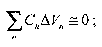
- the present invention includes a clocking scheme such that the total net flow of holes in or out of the p-well 170 is always near zero. This statement is given as
- the timing of the four gates is shown in Fig. 4. If the time interval from time T1 to time T2 is examined, it is readily apparent that V 1 and V2 have a positive transition. At the same time, V3 and V4 have an equal but opposite negative transition. This is true for each time interval. Every positive going clock edge on one phase is compensated by a negative going edge on one or more other phases. By utilizing compensated clock edges there is no net flow of holes through the p-well 170. With no need to wait for holes to flow through the p-well 170, the CCD gate phases may be clocked more rapidly and returned back to their accumulated state.
- the present invention keeps the CCD gate phases in the accumulated state for a longer period of time than in the prior art.
- the accumulated state lowers the thermal generation rate of unwanted electrons.
- the present invention also applies to CCD image sensor types of full frame, frame transfer, interline transfer, and frame interline transfer, and as stated above, it also applies to CCD types having three or more phases.
- FIG. 5 there is shown a digital camera 210 in which the CCD 150 may be inserted for implementing a commercial embodiment of the present invention. Although a digital camera is shown, other image capture devices such as satellite imaging, video imaging and the like may implement the present invention.
Landscapes
- Engineering & Computer Science (AREA)
- Multimedia (AREA)
- Signal Processing (AREA)
- Solid State Image Pick-Up Elements (AREA)
- Transforming Light Signals Into Electric Signals (AREA)
Abstract
Description
- The invention relates generally to the field of charge-coupled devices and, more particularly, to such charge-coupled devices having substantially no capacitance when in the accumulation mode.
- As shown in Fig. 1, prior art charge-coupled
devices 10 typically include a substrate or well 20 of the first conductivity type and buriedchannel 30 of the second conductivity type for the transfer ofcharge packets 40. A plurality ofgates 50 are separated from the buriedchannel 30 by a thininsulating layer 60. For the purpose of illustration, it is assumed that the first conductivity type is p-type and the second conductivity type is n-type. Thecharge packets 40 are electrons flowing in the n-type buriedchannel 30. The opposite type of theelectron charge packets 40 will be holes flowing in the p-type substrate or well 20. - Voltages applied to the
gates 50 alter the potential energy within the buriedchannel 30 for the purpose of controlling the transfer ofcharge packets 40 through the charge-coupleddevice 10. Additional p-type implants 70 are used to selectively alter the channel potential under thegates 50 for controlling the direction ofcharge packet 40 transfer. - If the
CCD 10 is to be used as an imaging device, then thecharge packets 40 transferred through the buriedchannel 30 were generated by photons. The photo-generated electrons in thecharge packets 40 are called photoelectrons. In the case of full frame type image sensors, the photoelectrons are generated directly in the CCD. In the case of interline frame transfer image sensors, the photoelectrons are generated in photodiodes adjacent to the CCD. There are also undesired electrons generated in the charge packets by thermal processes. These thermally generated electrons degrade the charge packet signal quality. It is well known that the thermal generation rate of electrons may be reduced by maintaining thegates 50 at a negative voltage with respect to the well orsubstrate 20. This causes holes to accumulate at the surface of the buriedchannel 30. The abundance of holes at the surface suppresses the thermal generation of electrons.Gates 50 biased to maintain holes at the surface are said to be in accumulation.Gates 50 biased such that holes are not present at the surface are said to be in depletion. A description of the benefits of accumulation mode clocking of CCD's may be found in U.S. Pat 4,963,952 by Janesick and in Solid - State Imaging with Charge-Coupled Devices by Albert J.P. Theuwissen. - In Fig. 1, at time T1 all
gate 50 voltages are at the low level which accumulates holes at the surface of the buriedchannel 30. At time T1, the thermal generation of dark current is lowest. To move thecharge packets 40, thegates 50 must be clocked. The CCD shown in Fig. 1 is a two phase CCD. It has two sets of gates, thefirst set 51 is clocked at voltage V1 and thesecond set 52 is clocked at voltage V2. The clocking sequence of the voltages V1 and V2 are shown in Fig. 1. It is well understood that CCDs may be fabricated with more than two sets of gates. - The
gate 50 clocking scheme of U.S. Pat. 4,963,952 is sufficient for CCDs built in p-type substrates. The p-type substrate acts as a source or sink ofholes as thegates 50 are clocked between accumulation and depletion voltages. However, as shown in Fig. 2 many interline CCD image sensors are built on n-type substrates 100 with p-type wells 20. Thewell 20 is confined in a narrow layer between thesubstrate 100 and buriedchannel 30. Now the well 20 can not easily act as a source or sink of holes. When thegates 50 are clocked into accumulation, the holes must flow long distances from the wellcontact 110 at the perimeter of the CCD to the center of the CCD. Thewell 20 has a high resistance to the flow of holes. Thenth gate 50 has a capacitance to the well 20 given by Cn. The well 20 has a resistance from the wellcontact 110 to the nth gate given by Rn. When thenth gate 50 is clocked into accumulation or depletion, the time it takes for holes to flow from the wellcontact 110 will be related to the product of Cn Rn. For large area CCDs, this time becomes so long that it limits the advantage of accumulation mode clocking. - One solution to this problem is described in U.S. Pat. 5,151,380. This patent discloses adding more
well contacts 110 with a low resistance metal throughout the entire area of the CCD. While the low resistance metal would certainly speed up the flow of holes in and out of thewell 20, it adds significant complexity to the manufacturing process. Theadditional contacts 110 to the well 20 in close proximity to the CCD also introduces impurities to the buriedchannel 30 which increases the thermal generation of electrons. The presence of the low resistance metal may also block photons from reaching the photosensitive. area of the CCD. - Consequently, it is clear that there is a need for a method of clocking a CCD in accumulation mode that does not require holes to travel long distances. In addition, it is also desirable for the method to apply to CCD's having more than two phases.
- The present invention is directed to overcoming one or more of the problems set forth above. Briefly summarized, according to one aspect of the present invention, the invention resides in A method for reducing dark current within a charge coupled device comprising the steps of: (a) providing three or more phases of gates separated by an insulating layer from a buried channel of the first conductivity type in a well or substrate of the second conductivity type, and a clock driver for causing the transfer of charge through the charge coupled device; (b) providing a barrier for separating charge packets when in accumulation state; (c) applying, at a first time period, voltages to all phases of gates sufficient to cause the surface of the first conductivity type to be accumulated by dark current reducing charge carriers; after the first time period, applying, at each gate phase n having a capacitance Cn to the layer of the second conductivity type, a voltage change on the gate phase n given by ΔVn such that the sum of products of the capacitances and voltage changes is substantially zeroand after the voltage changes required to transfer charge through the charge coupled device, returning the voltages of all phases of gates back to the voltage sufficient to cause the surface of the first conductivity type to be accumulated by dark current reducing charge carriers.

- These and other aspects, objects, features and advantages of the present invention will be more clearly understood and appreciated from a review of the following detailed description of the preferred embodiments and appended claims, and by reference to the accompanying drawings.
- The present invention has the advantage of reducing dark current, particularly in a three or more phase device, by enabling holes to flow more freely in accumulation without the need for additional contacts, which are undesirable as described hereinabove.
- Fig. 1 is a side view in vertical cross section of a prior art CCD and its associated clocking and energy transfer diagrams;
- Fig. 2 is a side view in vertical cross section of another prior art CCD;
- Fig. 3 is a side view in vertical cross section of a CCD of the present invention and its associated transfer diagrams;
- Fig. 4 is a diagram of the clocking for the CCD of Fig. 3; and
- Fig. 5 is a perspective view of a digital camera for implementing a typical commercial embodiment of the present invention.
-
- Referring to Fig. 3, there is shown a four
phase CCD 150 of the present invention. A four phase CCD is selected for exemplary purposes of a preferred embodiment. It will be readily apparent to those skilled in the art that the invention will apply to any CCD having three or more phases. TheCCD 150 has four sets of gates identified as V1, V2, V3, and V4. TheCCD 150 also includes an n-type buriedchannel 160 in a p-type well 170 on an n-type substrate 180. Charge packets of electrons 190 are confined within the buriedchannel 160. P-type implants 200 are selectively placed under predetermined gates in order to keep thecharge packets 200 separated when all the gates are in accumulation. - The present invention includes a means of clocking the CCD gates without the requirement of holes flowing through the p-well 170. It is instructive to note that Cn is designated as the capacitance of CCD gate phase n to the p-
well 170. At any given time, ΔVn is designated as the change in voltage of CCD gate phase n, and ΔQn is designated as the amount of charge represented by the holes under CCD gate phase n which must flow into or out of the p-well 170 when the gate voltage is changed by ΔVn . When ΔVn is positive, hole charge must flow away from the buriedchannel 160 surface into the p-well 170. When ΔVn is negative, hole charge must flow from the p-well 170 to the buriedchannel surface 160. The amount of the charge under phase n given by the equation - The present invention includes a clocking scheme such that the total net flow of holes in or out of the p-well 170 is always near zero. This statement is given as

- Continuing with the four phase example of Fig. 4, the timing of the four gates is shown in Fig. 4. If the time interval from time T1 to time T2 is examined, it is readily apparent that V 1 and V2 have a positive transition. At the same time, V3 and V4 have an equal but opposite negative transition. This is true for each time interval. Every positive going clock edge on one phase is compensated by a negative going edge on one or more other phases. By utilizing compensated clock edges there is no net flow of holes through the p-well 170. With no need to wait for holes to flow through the p-well 170, the CCD gate phases may be clocked more rapidly and returned back to their accumulated state. The present invention keeps the CCD gate phases in the accumulated state for a longer period of time than in the prior art. The accumulated state lowers the thermal generation rate of unwanted electrons. The present invention also applies to CCD image sensor types of full frame, frame transfer, interline transfer, and frame interline transfer, and as stated above, it also applies to CCD types having three or more phases.
- Referring to Fig. 5, there is shown a
digital camera 210 in which theCCD 150 may be inserted for implementing a commercial embodiment of the present invention. Although a digital camera is shown, other image capture devices such as satellite imaging, video imaging and the like may implement the present invention.
Claims (2)
- A method for reducing dark current within a charge coupled device, the method comprising the steps of:providing three or more phases of gates separated by an insulating layer from a buried channel of the first conductivity type in a well or substrate of the second conductivity type, and a clock driver for causing the transfer of charge through the charge coupled device;providing a barrier for separating charge packets when in accumulation state;applying, at a first time period, voltages to all phases of gates sufficient to cause the surface of the first conductivity type to be accumulated by dark current reducing charge carriers;after the first time period, applying, at each gate phase n having a capacitance Cn to the layer of the second conductivity type, a voltage change on the gate phase n given by ΔVn such that the sum of products of the capacitances and voltage changes is substantially zero
 after the voltage changes required to transfer charge through the charge coupled device, returning the voltages of all phases of gates back to the voltage sufficient to cause the surface of the first conductivity type to be accumulated by dark current reducing charge carriers.
 - A camera comprising:wherein at a first time period, voltages to all phases of the gates are sufficient to cause the surface of the first conductivity type to be accumulated by dark current reducing charge carriers;(a) a charge coupled device which reduces dark current within the charge-coupled device;
the charge coupled device comprising:(b) three or more phases of gates separated by an insulating layer from a buried channel of the first conductivity type in a well or substrate of the second conductivity type, and a clock driver for causing the transfer of charge through the charge coupled device;(c) a barrier for separating charge packets when in accumulation state;
wherein after the first time period, at each gate phase n having a capacitance Cn to the layer of the second conductivity type, a voltage change on the gate phase n given by ΔVn is such that the sum of products of the capacitances and voltage changes is substantially zeroand wherein after the voltage changes required to transfer charge through the charge coupled device, the voltages of all phases of gates returns back to the voltage sufficient to cause the surface of the first conductivity type to be accumulated by dark current reducing charge carriers.
Applications Claiming Priority (2)
| Application Number | Priority Date | Filing Date | Title |
|---|---|---|---|
| US10/263,169 US6586784B1 (en) | 2002-10-02 | 2002-10-02 | Accumulation mode clocking of a charge-coupled device |
| US263169 | 2002-10-02 |
Publications (3)
| Publication Number | Publication Date |
|---|---|
| EP1406305A2 true EP1406305A2 (en) | 2004-04-07 |
| EP1406305A3 EP1406305A3 (en) | 2008-04-30 |
| EP1406305B1 EP1406305B1 (en) | 2009-08-26 |
Family
ID=23000680
Family Applications (1)
| Application Number | Title | Priority Date | Filing Date |
|---|---|---|---|
| EP03077990A Expired - Lifetime EP1406305B1 (en) | 2002-10-02 | 2003-09-22 | Method of operating a charge-coupled device (CCD) |
Country Status (4)
| Country | Link |
|---|---|
| US (1) | US6586784B1 (en) |
| EP (1) | EP1406305B1 (en) |
| JP (1) | JP2004129256A (en) |
| DE (1) | DE60328949D1 (en) |
Families Citing this family (11)
| Publication number | Priority date | Publication date | Assignee | Title |
|---|---|---|---|---|
| US7015520B1 (en) * | 2004-10-13 | 2006-03-21 | Eastman Kodak Company | Charge-coupled devices having efficient charge transfer rates |
| US7952633B2 (en) * | 2004-11-18 | 2011-05-31 | Kla-Tencor Technologies Corporation | Apparatus for continuous clocking of TDI sensors |
| US7880782B2 (en) * | 2008-05-30 | 2011-02-01 | Eastman Kodak Company | Image sensor clocking method |
| US7807955B2 (en) | 2008-05-30 | 2010-10-05 | Eastman Kodak Company | Image sensor having reduced well bounce |
| US8803058B2 (en) | 2011-09-23 | 2014-08-12 | Truesense Imaging, Inc. | Multiple clocking modes for a CCD imager |
| US8735794B2 (en) | 2011-09-23 | 2014-05-27 | Truesense Imaging, Inc. | Multiple clocking modes for a CCD imager |
| US8723098B2 (en) | 2011-09-23 | 2014-05-13 | Truesense Imaging, Inc. | Charge coupled image sensor and method of operating with transferring operation of charge packets from plural photodetectors to vertical CCD shift registers (as amended) |
| WO2013043788A1 (en) | 2011-09-23 | 2013-03-28 | Truesense Imaging, Inc. | Multiple clocking modes for a ccd imager |
| US8830372B2 (en) | 2011-09-23 | 2014-09-09 | Semiconductor Components Industries, Llc | CCD image sensor having multiple clocking modes |
| US9848142B2 (en) | 2015-07-10 | 2017-12-19 | Semiconductor Components Industries, Llc | Methods for clocking an image sensor |
| FR3108784B1 (en) * | 2020-03-30 | 2022-04-01 | St Microelectronics Crolles 2 Sas | Charge Coupled Device |
Citations (1)
| Publication number | Priority date | Publication date | Assignee | Title |
|---|---|---|---|---|
| EP0917207A1 (en) | 1997-11-14 | 1999-05-19 | Thomson-Csf | Semiconductor charge transfer device |
Family Cites Families (7)
| Publication number | Priority date | Publication date | Assignee | Title |
|---|---|---|---|---|
| JPS58154269A (en) * | 1982-03-09 | 1983-09-13 | Matsushita Electronics Corp | Charge transfer device |
| US4963952C1 (en) | 1989-03-10 | 2001-07-31 | California Inst Of Techn | Multipinned phase charge-coupled device |
| US5151380A (en) | 1991-08-19 | 1992-09-29 | Texas Instruments Incorporated | Method of making top buss virtual phase frame interline transfer CCD image sensor |
| JPH06314706A (en) * | 1993-04-30 | 1994-11-08 | Nec Corp | Charge transfer device, driving method thereof and manufacturing method thereof |
| US5703642A (en) * | 1994-09-30 | 1997-12-30 | Eastman Kodak Company | Full depletion mode clocking of solid-state image sensors for improved MTF performance |
| JP2768311B2 (en) * | 1995-05-31 | 1998-06-25 | 日本電気株式会社 | Charge transfer device |
| JP2001308313A (en) * | 2000-04-21 | 2001-11-02 | Nec Corp | Charge transfer device and solid-state imaging device using the same |
-
2002
- 2002-10-02 US US10/263,169 patent/US6586784B1/en not_active Expired - Lifetime
-
2003
- 2003-09-22 DE DE60328949T patent/DE60328949D1/en not_active Expired - Lifetime
- 2003-09-22 EP EP03077990A patent/EP1406305B1/en not_active Expired - Lifetime
- 2003-09-25 JP JP2003332759A patent/JP2004129256A/en active Pending
Patent Citations (1)
| Publication number | Priority date | Publication date | Assignee | Title |
|---|---|---|---|---|
| EP0917207A1 (en) | 1997-11-14 | 1999-05-19 | Thomson-Csf | Semiconductor charge transfer device |
Also Published As
| Publication number | Publication date |
|---|---|
| US6586784B1 (en) | 2003-07-01 |
| JP2004129256A (en) | 2004-04-22 |
| DE60328949D1 (en) | 2009-10-08 |
| EP1406305B1 (en) | 2009-08-26 |
| EP1406305A3 (en) | 2008-04-30 |
Similar Documents
| Publication | Publication Date | Title |
|---|---|---|
| US9848142B2 (en) | Methods for clocking an image sensor | |
| KR100262774B1 (en) | Top bus virtual phase frame interline transfer ccd image sensor | |
| CN103650479B (en) | Solid-state imaging device, driving method thereof, manufacturing method, and electronic device | |
| EP1081766A1 (en) | CCD image sensor using amplification by secondary electron generation | |
| US6995795B1 (en) | Method for reducing dark current | |
| EP1406305A2 (en) | Charge-coupled device (CCD) and method of operating the same | |
| KR100880528B1 (en) | CMOS image sensor | |
| KR960004467B1 (en) | Solid state imaging device | |
| US5703642A (en) | Full depletion mode clocking of solid-state image sensors for improved MTF performance | |
| JPH08181300A (en) | Imaging device | |
| JP2007520063A (en) | Image sensor having p-type well with reduced conductivity | |
| US7184083B2 (en) | Solid state image pickup apparatus of low power consumption and its driving method | |
| JPH0775020A (en) | Charge coupled device | |
| US7880782B2 (en) | Image sensor clocking method | |
| Bosiers et al. | An S-VHS compatible 1/3" color FT-CCD imager with low dark current by surface pinning | |
| Parks et al. | Large-area interline CCD with low-dark current | |
| JP2758739B2 (en) | Driving method of solid-state imaging device | |
| Theuwissen et al. | The hole role | |
| US20250160027A1 (en) | Solid-state imaging element | |
| Nichols et al. | High‐resolution interline image sensors using two‐phase CCD technology | |
| US20060033830A1 (en) | Solid-state imaging device and its driving method for preventing damage in dynamic range | |
| JP4069475B2 (en) | Charge detection device, charge transfer device equipped with the same, and solid-state imaging device | |
| KR0151181B1 (en) | Structure of ccd image sensor | |
| JPH09181292A (en) | Solid state image pickup element and its drive method | |
| JPH03228373A (en) | Solid state image pickup device |
Legal Events
| Date | Code | Title | Description |
|---|---|---|---|
| PUAI | Public reference made under article 153(3) epc to a published international application that has entered the european phase |
Free format text: ORIGINAL CODE: 0009012 |
|
| AK | Designated contracting states |
Kind code of ref document: A2 Designated state(s): AT BE BG CH CY CZ DE DK EE ES FI FR GB GR HU IE IT LI LU MC NL PT RO SE SI SK TR |
|
| AX | Request for extension of the european patent |
Extension state: AL LT LV MK |
|
| PUAL | Search report despatched |
Free format text: ORIGINAL CODE: 0009013 |
|
| AK | Designated contracting states |
Kind code of ref document: A3 Designated state(s): AT BE BG CH CY CZ DE DK EE ES FI FR GB GR HU IE IT LI LU MC NL PT RO SE SI SK TR |
|
| AX | Request for extension of the european patent |
Extension state: AL LT LV MK |
|
| 17P | Request for examination filed |
Effective date: 20080911 |
|
| 17Q | First examination report despatched |
Effective date: 20081008 |
|
| AKX | Designation fees paid |
Designated state(s): DE FR GB |
|
| GRAP | Despatch of communication of intention to grant a patent |
Free format text: ORIGINAL CODE: EPIDOSNIGR1 |
|
| RTI1 | Title (correction) |
Free format text: METHOD OF OPERATING A CHARGE-COUPLED DEVICE (CCD) |
|
| GRAS | Grant fee paid |
Free format text: ORIGINAL CODE: EPIDOSNIGR3 |
|
| GRAA | (expected) grant |
Free format text: ORIGINAL CODE: 0009210 |
|
| AK | Designated contracting states |
Kind code of ref document: B1 Designated state(s): DE FR GB |
|
| REG | Reference to a national code |
Ref country code: GB Ref legal event code: FG4D |
|
| REF | Corresponds to: |
Ref document number: 60328949 Country of ref document: DE Date of ref document: 20091008 Kind code of ref document: P |
|
| PLBE | No opposition filed within time limit |
Free format text: ORIGINAL CODE: 0009261 |
|
| STAA | Information on the status of an ep patent application or granted ep patent |
Free format text: STATUS: NO OPPOSITION FILED WITHIN TIME LIMIT |
|
| 26N | No opposition filed |
Effective date: 20100527 |
|
| REG | Reference to a national code |
Ref country code: GB Ref legal event code: 732E Free format text: REGISTERED BETWEEN 20120315 AND 20120321 |
|
| REG | Reference to a national code |
Ref country code: DE Ref legal event code: R082 Ref document number: 60328949 Country of ref document: DE Representative=s name: MEYER & PARTNER GBR, DE |
|
| REG | Reference to a national code |
Ref country code: GB Ref legal event code: 732E Free format text: REGISTERED BETWEEN 20140904 AND 20140910 |
|
| REG | Reference to a national code |
Ref country code: DE Ref legal event code: R081 Ref document number: 60328949 Country of ref document: DE Owner name: SEMICONDUCTOR COMPONENTS INDUSTRIES, LLC (N. D, US Free format text: FORMER OWNER: EASTMAN KODAK CO., ROCHESTER, N.Y., US Effective date: 20140918 Ref country code: DE Ref legal event code: R082 Ref document number: 60328949 Country of ref document: DE Representative=s name: MEYER & PARTNER GBR, DE Effective date: 20140918 |
|
| PGFP | Annual fee paid to national office [announced via postgrant information from national office to epo] |
Ref country code: FR Payment date: 20140906 Year of fee payment: 12 |
|
| REG | Reference to a national code |
Ref country code: FR Ref legal event code: ST Effective date: 20160531 |
|
| PG25 | Lapsed in a contracting state [announced via postgrant information from national office to epo] |
Ref country code: FR Free format text: LAPSE BECAUSE OF NON-PAYMENT OF DUE FEES Effective date: 20150930 |
|
| PGFP | Annual fee paid to national office [announced via postgrant information from national office to epo] |
Ref country code: DE Payment date: 20190820 Year of fee payment: 17 |
|
| PGFP | Annual fee paid to national office [announced via postgrant information from national office to epo] |
Ref country code: GB Payment date: 20190820 Year of fee payment: 17 |
|
| REG | Reference to a national code |
Ref country code: DE Ref legal event code: R119 Ref document number: 60328949 Country of ref document: DE |
|
| GBPC | Gb: european patent ceased through non-payment of renewal fee |
Effective date: 20200922 |
|
| PG25 | Lapsed in a contracting state [announced via postgrant information from national office to epo] |
Ref country code: DE Free format text: LAPSE BECAUSE OF NON-PAYMENT OF DUE FEES Effective date: 20210401 |
|
| PG25 | Lapsed in a contracting state [announced via postgrant information from national office to epo] |
Ref country code: GB Free format text: LAPSE BECAUSE OF NON-PAYMENT OF DUE FEES Effective date: 20200922 |