EP1403931A2 - Method for growing a silicon film, method for manufacturing a solar cell, semiconductor substrate, and solar cell - Google Patents
Method for growing a silicon film, method for manufacturing a solar cell, semiconductor substrate, and solar cell Download PDFInfo
- Publication number
- EP1403931A2 EP1403931A2 EP03021944A EP03021944A EP1403931A2 EP 1403931 A2 EP1403931 A2 EP 1403931A2 EP 03021944 A EP03021944 A EP 03021944A EP 03021944 A EP03021944 A EP 03021944A EP 1403931 A2 EP1403931 A2 EP 1403931A2
- Authority
- EP
- European Patent Office
- Prior art keywords
- silicon film
- silicon
- solar cell
- semiconductor substrate
- growing
- Prior art date
- Legal status (The legal status is an assumption and is not a legal conclusion. Google has not performed a legal analysis and makes no representation as to the accuracy of the status listed.)
- Withdrawn
Links
Images

Classifications
-
- H—ELECTRICITY
- H10—SEMICONDUCTOR DEVICES; ELECTRIC SOLID-STATE DEVICES NOT OTHERWISE PROVIDED FOR
- H10F—INORGANIC SEMICONDUCTOR DEVICES SENSITIVE TO INFRARED RADIATION, LIGHT, ELECTROMAGNETIC RADIATION OF SHORTER WAVELENGTH OR CORPUSCULAR RADIATION
- H10F10/00—Individual photovoltaic cells, e.g. solar cells
- H10F10/10—Individual photovoltaic cells, e.g. solar cells having potential barriers
- H10F10/14—Photovoltaic cells having only PN homojunction potential barriers
-
- H—ELECTRICITY
- H10—SEMICONDUCTOR DEVICES; ELECTRIC SOLID-STATE DEVICES NOT OTHERWISE PROVIDED FOR
- H10F—INORGANIC SEMICONDUCTOR DEVICES SENSITIVE TO INFRARED RADIATION, LIGHT, ELECTROMAGNETIC RADIATION OF SHORTER WAVELENGTH OR CORPUSCULAR RADIATION
- H10F71/00—Manufacture or treatment of devices covered by this subclass
- H10F71/121—The active layers comprising only Group IV materials
-
- H—ELECTRICITY
- H10—SEMICONDUCTOR DEVICES; ELECTRIC SOLID-STATE DEVICES NOT OTHERWISE PROVIDED FOR
- H10F—INORGANIC SEMICONDUCTOR DEVICES SENSITIVE TO INFRARED RADIATION, LIGHT, ELECTROMAGNETIC RADIATION OF SHORTER WAVELENGTH OR CORPUSCULAR RADIATION
- H10F77/00—Constructional details of devices covered by this subclass
- H10F77/10—Semiconductor bodies
- H10F77/14—Shape of semiconductor bodies; Shapes, relative sizes or dispositions of semiconductor regions within semiconductor bodies
-
- Y—GENERAL TAGGING OF NEW TECHNOLOGICAL DEVELOPMENTS; GENERAL TAGGING OF CROSS-SECTIONAL TECHNOLOGIES SPANNING OVER SEVERAL SECTIONS OF THE IPC; TECHNICAL SUBJECTS COVERED BY FORMER USPC CROSS-REFERENCE ART COLLECTIONS [XRACs] AND DIGESTS
- Y02—TECHNOLOGIES OR APPLICATIONS FOR MITIGATION OR ADAPTATION AGAINST CLIMATE CHANGE
- Y02E—REDUCTION OF GREENHOUSE GAS [GHG] EMISSIONS, RELATED TO ENERGY GENERATION, TRANSMISSION OR DISTRIBUTION
- Y02E10/00—Energy generation through renewable energy sources
- Y02E10/50—Photovoltaic [PV] energy
- Y02E10/547—Monocrystalline silicon PV cells
-
- Y—GENERAL TAGGING OF NEW TECHNOLOGICAL DEVELOPMENTS; GENERAL TAGGING OF CROSS-SECTIONAL TECHNOLOGIES SPANNING OVER SEVERAL SECTIONS OF THE IPC; TECHNICAL SUBJECTS COVERED BY FORMER USPC CROSS-REFERENCE ART COLLECTIONS [XRACs] AND DIGESTS
- Y02—TECHNOLOGIES OR APPLICATIONS FOR MITIGATION OR ADAPTATION AGAINST CLIMATE CHANGE
- Y02P—CLIMATE CHANGE MITIGATION TECHNOLOGIES IN THE PRODUCTION OR PROCESSING OF GOODS
- Y02P70/00—Climate change mitigation technologies in the production process for final industrial or consumer products
- Y02P70/50—Manufacturing or production processes characterised by the final manufactured product
Definitions
- the present invention relates to a solar cell having an uneven light confining structure, a semiconductor substrate which is preferably used as a component for the solar cell, and a manufacturing method therefor. More particularly, the present invention relates to a solar cell utilizing a silicon film formed on a substrate by a liquid phase epitaxy, a semiconductor substrate which is preferably used as a component for the solar cell, and a manufacturing method therefor.
- Japanese Patent Application Laid-Open No. 03-023678 (whose patent application was filed by Mitsubishi Electric Corporation) describes a structure in which a number of cylindrical light receiving surfaces are formed on a flat light receiving surface so that incident light is introduced into a dead end in the cylinder.
- Japanese Patent Application Laid-Open No. 62-101084 discloses a light confining solar cell having a concave space which has capability of confining at least a part of incident light in the surface portion of the solar cell.
- the present invention has been made in view of solving the above-mentioned problems. Therefore, it is an object of the present invention to provide a solar cell having a light confining structure capable of effectively confining light such as a dead end structure and being less expensive, and a semiconductor substrate which is preferably used as a component for the solar cell.
- the present invention has been accomplished in order to effectively attain the above-mentioned objects and the present invention is to provide a method for growing a silicon film by liquid phase epitaxy on a surface of a substrate in contact with a solution containing at least silicon by decreasing a temperature of the solution, comprising the steps of: forming a bulk portion having substantially no void; and forming a surface portion having plural protrusions that overhang in a lateral direction.
- a method for manufacturing a solar cell according to the present invention includes forming a P-N junction on the silicon film.
- a semiconductor substrate according to the present invention comprises an inclined plane and plural grooves of a gap portion communicated with the inclined plane on a surface layer composed of silicon.
- a semiconductor substrate according to the present invention comprises a surface portion having an inclined plane affected by a crystal structure of silicon and plural protrusions that overhang in a lateral direction in a surface layer composed of silicon, in which plural grooves having openings narrowed due to the protrusions overhanging in the lateral direction are formed on the surface portion.
- a solar cell according to the present invention comprises a semiconductor substrate described above as a component, in which a P-N junction is formed on a surface layer composed of silicon.
- a solar cell comprises a semiconductor substrate having an inclined plane and plural grooves of a gap portion communicated with the inclined plane on a surface layer composed of silicon, and a collector electrode crossing over the plural grooves on the semiconductor substrate.
- Fig. 1 is a schematic cross-sectional view illustrating an embodiment of a silicon film according to the present invention by use of a cross-sectional picture of the silicon film.
- Fig. 1 indicates that a silicon film 2, which is a characteristic component of the present invention, is formed on a substrate 1.
- the silicon film 2 in the present invention includes a bulk portion 2a and a surface portion 2b.
- the bulk portion 2a includes substantially no void in a cross-sectional view.
- the surface portion 2b includes plural protrusions that overhang (overhangs 3) in a lateral direction.
- the phrase "substantially no voids” means the case that there exist no voids at all or the case that the number of a minute void which appears in the cross section is one void/cm 2 or less.
- minute void which appears in the cross section means, for example, a void having a spherical diameter of 0.1 ⁇ m or more when the void is regarded as an equivalent of a sphere.
- Such a structure is obtained by growing protrusions that overhang in a lateral direction at the final stage of a liquid phase growth method which epitaxially grows the silicon film 2 on the substrate 1.
- a liquid phase growth method which epitaxially grows the silicon film 2 on the substrate 1.
- a method for obtaining the structure includes, a method which includes decreasing the temperature of the system at a constant rate, and a method which includes decreasing the temperature of the system while a temperature decreasing rate is stepwise or continuously increased.
- a method which includes decreasing the temperature of the system at a constant rate it is preferred that supersaturation temperature is 5 to 15°C, a temperature decreasing rate is 0.2 to 2°C/minute, and a growth time is 30 to 120 minutes.
- the latter method is preferably applicable. More specifically, the following process is performed.
- a temperature decreasing rate of a solution is set to be small to grow a crystal so that the bulk portion is formed by flat growth.
- a temperature decreasing rate of the solution is set to be large to grow the crystal so that the surface portion is formed by facet growth.
- the supersaturation temperature is 2 to 14°C
- a temperature decreasing rate is 0 to 0.2°C/minute
- a growth time is 10 to 60 minutes.
- a temperature decreasing rate is 0.2 to 2°C/minute
- a growth time is 30 to 120 minutes. It is more preferred that a temperature decreasing rate be increased stepwise in the step of forming the surface portion.
- growth conditions are generally regulated by a feeding rate of a silicon material (a crystal material) to a substrate. More specifically, growth conditions are appropriately set depending on the kind or a volume of a solution, a material dissolving temperature, the supersaturation temperature, a temperature decreasing rate, and spacing between substrates.
- a silicon film 2 which includes a bulk portion 2a having a thickness of approximately 20 ⁇ m and a surface portion 2b having protrusions of approximately 60 ⁇ m in height, is obtained.
- the overhangs 3 in a lateral direction have planes of almost the same inclination.
- the planes having almost the same inclination are formed not only on the surface side but also on the lower side of the respective overhangs 3 (i.e., the plane including a gap portion). It is conceivable that this is due to (111) surface or (100) surface which is predominant at the growth of the surface portion 2b.
- the gap portion formed on the lower side of the overhang 3 shown in Fig. 1 continuously extends in a direction perpendicular to the drawing sheet. In other words, a groove 5 having a dead end shape is formed on the surface.
- the width of an opening of the groove may be controlled to be 0.1 to 50 ⁇ m and the vertical depth from the opening to the deepest end of the groove may be controlled to be 5 to 100 ⁇ m. Furthermore, a void 4, which does not communicate with the outside, may be formed at the inside of the silicon film 2 by connection of the adjacent overhangs.
- the width of the opening of the groove By controlling the width of the opening of the groove to be in the range of 0.1 to 50 ⁇ m, incident light would be introduced into the dead end of the groove so that reflection and absorption would be repeated in the groove. As a result, efficiency for light utilization would be increased. Furthermore, even in the case where a conductive paste is used for a collector electrode, the collector electrode would cross over the groove so as to prevent a cut off of the electrode. As a result, current collecting efficiency would be remarkably improved. Also, by controlling the vertical depth to be in the range of 5 to 100 ⁇ m, efficiency for light utilization would be increased as described above. Furthermore, a surface passivation effect due to an oxide film or a nitride film would be remarkably improved.
- a solar cell is manufactured by forming a P-N junction on a silicon film on which there exist "overhangs 3 in a lateral direction the planes of which having almost the same inclination (an inclined plane)" which can be formed by the above-mentioned growth method. Therefore, it is possible to manufacture a solar cell having capability of more effectively introducing incident light into a dead end of a groove compared to a conventional solar cell merely having a dead end structure on the surface thereof. As a result, it is possible to further increase efficiency for light utilization of a solar cell.
- inexpensive multicrystalline silicon can be used as the substrate 1. Furthermore, since a solar cell according to the present invention utilizes the silicon film 2 as a photoactive layer, especially inexpensive metallurgical grade multicrystalline silicon can be used as the result.
- metallurgical grade silicon means silicon obtained by directly reducing a silica sand. Such silicon usually has purity of less than 99.99%, but it is far inexpensive compared to semiconductor class silicon or solar cell class silicon.
- the substrate is washed with a mixed liquid of sulfuric acid and hydrogen peroxide and subjected to a so-called planar etching (a flattening treatment) using mixed acid of hydrofluoric acid, nitric acid, and acetic acid prior to an epitaxial growth of a silicon film.
- FIG. 2 is a schematic cross-sectional view illustrating an example of a liquid phase epitaxial growth apparatus for forming the silicon film.
- a growth furnace 21 includes a crucible 22 therein and is surrounded by a heater 23.
- the crucible 22 contains a melt (a solution for crystal growth) 24 in which a silicon material is dissolved to be saturated in metal such as tin, indium, copper, or aluminum.
- a substrate loading chamber 26 is coupled to the upper portion of the growth furnace 21 through a gate valve 25.
- the substrate loading chamber 26 is horizontally slidable and includes a substrate holder 27 therein.
- a growth process is performed as follows.
- the gate valve 25 is closed, the growth furnace 21 is kept at the saturation temperature of the melt under hydrogen atmosphere.
- a substrate 28 is held on the substrate holder 27 while the substrate loading chamber 26 is separated from the growth furnace 21.
- the substrate loading chamber 26 is coupled to the growth furnace 21 and the inside thereof is replaced with hydrogen.
- the gate valve 25 is opened so that the substrate holder 27 lowered to be brought into the growth furnace 21 to heat the substrate 28 for a predetermined time under hydrogen atmosphere.
- the temperature of the growth furnace 21 is decreased to the extent that the silicon material in the melt 24 is supersaturated.
- the substrate holder 27 When the temperature of the furnace reaches the temperature at which a predetermined degree of supersaturation is attained, the substrate holder 27 is further lowered so that the substrate 28 is dipped in the melt 24. If the temperature of the growth furnace 21 is decreased at a predetermined temperature decreasing rate under the above-mentioned condition, then a silicon film is epitaxially grown on the substrate 28. When a desired silicon film is obtained, the substrate holder 27 is raised and the gate valve 25 is closed. Next, the inside of the substrate loading chamber 26 is replaced with air and the substrate loading chamber 26 is separated from the growth furnace 21 to take out the substrate 28.
- the melt 24 may contain a dopant such as gallium, phosphorous, boron or aluminum.
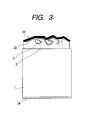
- Fig. 3 is a schematic cross-sectional view illustrating an embodiment of a solar cell according to the present invention.
- a P-type silicon film 2 is formed on a substrate 1 by the above-mentioned method.
- An n+ layer (not shown), an antireflection film 32, and a collector electrode 33 are formed on the surface of the silicon film 2.
- a back electrode 34 is formed on the back side of the substrate 1.
- the n+ layer can be formed by thermal diffusion, ion implantation or the like.
- the antireflection film 32 can be formed by sputtering, deposition, CVD, or the like using an oxide film or a nitride film.
- the collector electrode 33 and the back electrode 34 can be formed by sputtering, vapor deposition, printing, or the like using silver or aluminum.
- a solar cell according to another embodiment may include a hetero junction with an amorphous film on a multicrystalline silicon substrate. For example, a configuration in which an amorphous i layer and an amorphous n layer are laminated on a P-type silicon film 2 may be employed.
- An amorphous layer can be formed by, for example, a CVD method.
- the silicon film of the present invention includes plural protrusions that overhang in a lateral direction on the surface thereof. Many of the adjacent overhangs are separated from each other by a groove 5 having a dead end shape. Therefore, according to a solar cell of the present invention, it is possible to improve current collecting efficiency by forming a collector electrode 33 crossing over the groove 5 as shown in Fig. 3. At the portion where the collector electrode crosses over the groove 5, the collector electrode is arranged in midair.
- Applicable examples of a method of forming a collector electrode having such a structure include a method which includes applying a conductive paste having a relatively high viscosity onto a substrate and baking it, a method which further includes laminating metal having a low melting point such as solder on the baked paste, and a method which includes sticking a metal wire on the substrate with a conductive adhesive.
- a metallurgical grade multicrystalline silicon substrate having 47 mm length, 47 mm width and 0.6 mm thickness was used as a substrate.
- the substrate was washed with flowing water for 5 minutes and then dipped in a mixed liquid of sulfuric acid and hydrogen peroxide (mixed ratio of 3 to 1) for 10 minutes.
- the substrate was additionally washed with flowing water for 5 minutes and then dipped in a mixed liquid of nitric acid, acetic acid, and hydrofluoric acid (mixed ratio of 600/136/64) for 6 minutes and 30 seconds to perform a planar etching on the surface thereof.
- the substrate was washed with flowing water for 5 minutes and then dried by blowing dry nitrogen thereto, so as to complete a pre-treatment of the substrate.
- a silicon film was epitaxially grown on the above-mentioned metallurgical grade multicrystalline silicon substrate using a liquid phase growth apparatus as shown in Fig. 2.
- a melt 24 was prepared by dissolving and saturating a silicon material in 11 kg of indium at 900°C. The temperature of the melt was decreased to 886°C so as to produce a supersaturation condition. Then, the substrate 28 was dipped in the supersaturated melt. The substrate 28 was rotated at 10 rpm in the melt. The melt 24 was gradually cooled at a temperature decreasing rate of 0.1°C/minute for the initial 10 minutes, 0.5°C/minute for the next 10 minutes and 1.0°C/minute for the remaining 40 minutes.
- the silicon film included a bulk portion (20 ⁇ m thickness) and a surface portion (20 to 40 ⁇ m thickness) having plural protrusions that overhang in a lateral direction.
- a P-type silicon film 2 was formed by a liquid deposition method on a multicrystalline silicon substrate 1 according to the present invention, as described above.
- An N-type diffusion source was applied onto the surface of the silicon film 2 with a thickness of 2,000 angstroms and baked at 860°C to form an n+ layer (not shown).
- ITO was sputtered with a thickness of 820 angstroms to form an antireflection film 32.
- a silver paste was applied in a grid shape by a screen printing and then baked to form a collector electrode 33.
- a silver paste was applied onto the back side of the substrate 1 and baked to form a back electrode 34. As a result, a solar cell was obtained.
- a method for growing a silicon film of the present invention it is possible to form a silicon film having an uneven structure suitable for increasing optical path length on the surface of a semiconductor substrate without performing an additional process for forming an uneven structure. Therefore, it is possible to especially obtain a semiconductor substrate suitable for a solar cell having an improved short circuit current property at a low cost. As a result, it is possible to provide a solar cell having high efficiency and being low in price.
- a bulk portion having substantially no void is formed and then a surface portion having plural protrusions that overhang in a lateral direction is formed.
Landscapes
- Liquid Deposition Of Substances Of Which Semiconductor Devices Are Composed (AREA)
- Photovoltaic Devices (AREA)
- Crystals, And After-Treatments Of Crystals (AREA)
Abstract
Description
- The present invention relates to a solar cell having an uneven light confining structure, a semiconductor substrate which is preferably used as a component for the solar cell, and a manufacturing method therefor. More particularly, the present invention relates to a solar cell utilizing a silicon film formed on a substrate by a liquid phase epitaxy, a semiconductor substrate which is preferably used as a component for the solar cell, and a manufacturing method therefor.
- Conventionally, a technique in which an uneven light confining structure is formed on the surface of a solar cell to increase optical path length of incident light has been widely used. Japanese Patent Application Laid-Open No. 03-023678 (whose patent application was filed by Mitsubishi Electric Corporation) describes a structure in which a number of cylindrical light receiving surfaces are formed on a flat light receiving surface so that incident light is introduced into a dead end in the cylinder.
- Furthermore, Japanese Patent Application Laid-Open No. 62-101084 (whose patent application was filed by Sharp Corporation) discloses a light confining solar cell having a concave space which has capability of confining at least a part of incident light in the surface portion of the solar cell.
- It is conceivable that a light confining structure in which incident light is introduced into a dead end is significantly effective to increase short circuit current. However, the above-mentioned publications do not disclose or suggest a method of forming such structure individually or in combination.
- As an example of a method of forming an uneven structure in the surface layer of a solar cell, a method which mechanically grinds the surface of the solar cell by using a rotary grind-stone is known. However, according to this method using a rotary grind-stone, additional processes are required for forming an uneven structure which cause cost increase. Furthermore, according to this method, it is difficult to form the above-mentioned dead end structure.
- The present invention has been made in view of solving the above-mentioned problems. Therefore, it is an object of the present invention to provide a solar cell having a light confining structure capable of effectively confining light such as a dead end structure and being less expensive, and a semiconductor substrate which is preferably used as a component for the solar cell.
- It is also an object of the present invention to provide a method for manufacturing a solar cell having a structure capable of effectively confining light such as a dead end structure, which does not require additional processes for forming an uneven structure.
- The present invention has been accomplished in order to effectively attain the above-mentioned objects and the present invention is to provide a method for growing a silicon film by liquid phase epitaxy on a surface of a substrate in contact with a solution containing at least silicon by decreasing a temperature of the solution, comprising the steps of: forming a bulk portion having substantially no void; and forming a surface portion having plural protrusions that overhang in a lateral direction. Further, a method for manufacturing a solar cell according to the present invention includes forming a P-N junction on the silicon film. Further, a semiconductor substrate according to the present invention comprises an inclined plane and plural grooves of a gap portion communicated with the inclined plane on a surface layer composed of silicon. Further, a semiconductor substrate according to the present invention comprises a surface portion having an inclined plane affected by a crystal structure of silicon and plural protrusions that overhang in a lateral direction in a surface layer composed of silicon, in which plural grooves having openings narrowed due to the protrusions overhanging in the lateral direction are formed on the surface portion. Furthermore, a solar cell according to the present invention comprises a semiconductor substrate described above as a component, in which a P-N junction is formed on a surface layer composed of silicon. Further, a solar cell comprises a semiconductor substrate having an inclined plane and plural grooves of a gap portion communicated with the inclined plane on a surface layer composed of silicon, and a collector electrode crossing over the plural grooves on the semiconductor substrate.
-
- Fig. 1 is a schematic cross-sectional view illustrating an embodiment of a silicon film according to the present invention by use of a cross-sectional picture of the silicon film.
- Fig. 2 is a schematic side cross-sectional view illustrating an example of a liquid phase epitaxial growth apparatus for forming a silicon film according to the present invention.
- Fig. 3 is a schematic cross-sectional view illustrating an embodiment of a solar cell according to the present invention.
- Fig. 1 is a schematic cross-sectional view illustrating an embodiment of a silicon film according to the present invention by use of a cross-sectional picture of the silicon film.
- Fig. 1 indicates that a
silicon film 2, which is a characteristic component of the present invention, is formed on asubstrate 1. As shown in Fig. 1, thesilicon film 2 in the present invention includes abulk portion 2a and asurface portion 2b. Thebulk portion 2a includes substantially no void in a cross-sectional view. Thesurface portion 2b includes plural protrusions that overhang (overhangs 3) in a lateral direction. - In the present specification, the phrase "substantially no voids" means the case that there exist no voids at all or the case that the number of a minute void which appears in the cross section is one void/cm2 or less. Here, the phrase "minute void which appears in the cross section" means, for example, a void having a spherical diameter of 0.1 µm or more when the void is regarded as an equivalent of a sphere.
- Such a structure is obtained by growing protrusions that overhang in a lateral direction at the final stage of a liquid phase growth method which epitaxially grows the
silicon film 2 on thesubstrate 1. Although the mechanism by which such a structure is obtained is not clear, experiments performed by the present inventors suggest a phenomenon that a flat growth initially occurs, and overhanging of the protrusions in a lateral direction is initiated upon formation of a minute unevenness on the surface of the growing film. - A method for obtaining the structure includes, a method which includes decreasing the temperature of the system at a constant rate, and a method which includes decreasing the temperature of the system while a temperature decreasing rate is stepwise or continuously increased. In the case of a method which includes decreasing the temperature of the system at a constant rate, it is preferred that supersaturation temperature is 5 to 15°C, a temperature decreasing rate is 0.2 to 2°C/minute, and a growth time is 30 to 120 minutes. However, with this method, thickness of a bulk portion may be insufficient in some cases. Therefore, the latter method is preferably applicable. More specifically, the following process is performed. At the initial stage of liquid phase epitaxy (which is the step of forming a bulk portion), a temperature decreasing rate of a solution is set to be small to grow a crystal so that the bulk portion is formed by flat growth. Thereafter, in the step of forming a surface portion, a temperature decreasing rate of the solution is set to be large to grow the crystal so that the surface portion is formed by facet growth. In the step of forming the bulk portion, it is preferred that the supersaturation temperature is 2 to 14°C, a temperature decreasing rate is 0 to 0.2°C/minute, and a growth time is 10 to 60 minutes. In the step of forming the surface portion, it is preferred that a temperature decreasing rate is 0.2 to 2°C/minute, and a growth time is 30 to 120 minutes. It is more preferred that a temperature decreasing rate be increased stepwise in the step of forming the surface portion.
- However, growth conditions are generally regulated by a feeding rate of a silicon material (a crystal material) to a substrate. More specifically, growth conditions are appropriately set depending on the kind or a volume of a solution, a material dissolving temperature, the supersaturation temperature, a temperature decreasing rate, and spacing between substrates.
- For example, in the system where silicon is dissolved to be saturated in 11 kg of an In solution at 900°C to prepare a solution and a substrate is individually and vertically held in the solution to perform liquid phase epitaxy, if crystal growth is performed with the temperature of the solution for crystal growth being decreased to approximately 885°C to be supersaturated, a temperature decreasing rate after dipping the substrate being 0.2°C/minute, and a growth time being 150 minutes, then a
silicon film 2, which includes abulk portion 2a having a thickness of approximately 20 µm and asurface portion 2b having protrusions of approximately 60 µm in height, is obtained. - As is apparent from Fig. 1, in many cases, plural protrusions in the
surface portion 2b have characteristics that theoverhangs 3 in a lateral direction have planes of almost the same inclination. The planes having almost the same inclination are formed not only on the surface side but also on the lower side of the respective overhangs 3 (i.e., the plane including a gap portion). It is conceivable that this is due to (111) surface or (100) surface which is predominant at the growth of thesurface portion 2b. The gap portion formed on the lower side of theoverhang 3 shown in Fig. 1 continuously extends in a direction perpendicular to the drawing sheet. In other words, agroove 5 having a dead end shape is formed on the surface. The width of an opening of the groove may be controlled to be 0.1 to 50 µm and the vertical depth from the opening to the deepest end of the groove may be controlled to be 5 to 100 µm. Furthermore, a void 4, which does not communicate with the outside, may be formed at the inside of thesilicon film 2 by connection of the adjacent overhangs. - By controlling the width of the opening of the groove to be in the range of 0.1 to 50 µm, incident light would be introduced into the dead end of the groove so that reflection and absorption would be repeated in the groove. As a result, efficiency for light utilization would be increased. Furthermore, even in the case where a conductive paste is used for a collector electrode, the collector electrode would cross over the groove so as to prevent a cut off of the electrode. As a result, current collecting efficiency would be remarkably improved. Also, by controlling the vertical depth to be in the range of 5 to 100 µm, efficiency for light utilization would be increased as described above. Furthermore, a surface passivation effect due to an oxide film or a nitride film would be remarkably improved.
- Furthermore, according to the present invention, a solar cell is manufactured by forming a P-N junction on a silicon film on which there exist "
overhangs 3 in a lateral direction the planes of which having almost the same inclination (an inclined plane)" which can be formed by the above-mentioned growth method. Therefore, it is possible to manufacture a solar cell having capability of more effectively introducing incident light into a dead end of a groove compared to a conventional solar cell merely having a dead end structure on the surface thereof. As a result, it is possible to further increase efficiency for light utilization of a solar cell. - In the present invention, inexpensive multicrystalline silicon can be used as the
substrate 1. Furthermore, since a solar cell according to the present invention utilizes thesilicon film 2 as a photoactive layer, especially inexpensive metallurgical grade multicrystalline silicon can be used as the result. The term "metallurgical grade silicon" means silicon obtained by directly reducing a silica sand. Such silicon usually has purity of less than 99.99%, but it is far inexpensive compared to semiconductor class silicon or solar cell class silicon. In the case of using a metallurgical grade multicrystalline substrate, it is preferred that the substrate is washed with a mixed liquid of sulfuric acid and hydrogen peroxide and subjected to a so-called planar etching (a flattening treatment) using mixed acid of hydrofluoric acid, nitric acid, and acetic acid prior to an epitaxial growth of a silicon film. - A liquid phase epitaxy is used for obtaining a silicon film having an uneven structure on the surface thereof according to the present invention. Fig. 2 is a schematic cross-sectional view illustrating an example of a liquid phase epitaxial growth apparatus for forming the silicon film.
- A
growth furnace 21 includes a crucible 22 therein and is surrounded by aheater 23. The crucible 22 contains a melt (a solution for crystal growth) 24 in which a silicon material is dissolved to be saturated in metal such as tin, indium, copper, or aluminum. Asubstrate loading chamber 26 is coupled to the upper portion of thegrowth furnace 21 through a gate valve 25. Thesubstrate loading chamber 26 is horizontally slidable and includes asubstrate holder 27 therein. - A growth process is performed as follows. When the gate valve 25 is closed, the
growth furnace 21 is kept at the saturation temperature of the melt under hydrogen atmosphere. Asubstrate 28 is held on thesubstrate holder 27 while thesubstrate loading chamber 26 is separated from thegrowth furnace 21. Then thesubstrate loading chamber 26 is coupled to thegrowth furnace 21 and the inside thereof is replaced with hydrogen. Thereafter, the gate valve 25 is opened so that thesubstrate holder 27 lowered to be brought into thegrowth furnace 21 to heat thesubstrate 28 for a predetermined time under hydrogen atmosphere. Then, the temperature of thegrowth furnace 21 is decreased to the extent that the silicon material in the melt 24 is supersaturated. When the temperature of the furnace reaches the temperature at which a predetermined degree of supersaturation is attained, thesubstrate holder 27 is further lowered so that thesubstrate 28 is dipped in the melt 24. If the temperature of thegrowth furnace 21 is decreased at a predetermined temperature decreasing rate under the above-mentioned condition, then a silicon film is epitaxially grown on thesubstrate 28. When a desired silicon film is obtained, thesubstrate holder 27 is raised and the gate valve 25 is closed. Next, the inside of thesubstrate loading chamber 26 is replaced with air and thesubstrate loading chamber 26 is separated from thegrowth furnace 21 to take out thesubstrate 28. The melt 24 may contain a dopant such as gallium, phosphorous, boron or aluminum. - Fig. 3 is a schematic cross-sectional view illustrating an embodiment of a solar cell according to the present invention. A P-
type silicon film 2 is formed on asubstrate 1 by the above-mentioned method. An n+ layer (not shown), anantireflection film 32, and acollector electrode 33 are formed on the surface of thesilicon film 2. Aback electrode 34 is formed on the back side of thesubstrate 1. The n+ layer can be formed by thermal diffusion, ion implantation or the like. Theantireflection film 32 can be formed by sputtering, deposition, CVD, or the like using an oxide film or a nitride film. Thecollector electrode 33 and theback electrode 34 can be formed by sputtering, vapor deposition, printing, or the like using silver or aluminum. A solar cell according to another embodiment may include a hetero junction with an amorphous film on a multicrystalline silicon substrate. For example, a configuration in which an amorphous i layer and an amorphous n layer are laminated on a P-type silicon film 2 may be employed. An amorphous layer can be formed by, for example, a CVD method. - The silicon film of the present invention includes plural protrusions that overhang in a lateral direction on the surface thereof. Many of the adjacent overhangs are separated from each other by a
groove 5 having a dead end shape. Therefore, according to a solar cell of the present invention, it is possible to improve current collecting efficiency by forming acollector electrode 33 crossing over thegroove 5 as shown in Fig. 3. At the portion where the collector electrode crosses over thegroove 5, the collector electrode is arranged in midair. Applicable examples of a method of forming a collector electrode having such a structure include a method which includes applying a conductive paste having a relatively high viscosity onto a substrate and baking it, a method which further includes laminating metal having a low melting point such as solder on the baked paste, and a method which includes sticking a metal wire on the substrate with a conductive adhesive. - A metallurgical grade multicrystalline silicon substrate having 47 mm length, 47 mm width and 0.6 mm thickness was used as a substrate. The substrate was washed with flowing water for 5 minutes and then dipped in a mixed liquid of sulfuric acid and hydrogen peroxide (mixed ratio of 3 to 1) for 10 minutes. The substrate was additionally washed with flowing water for 5 minutes and then dipped in a mixed liquid of nitric acid, acetic acid, and hydrofluoric acid (mixed ratio of 600/136/64) for 6 minutes and 30 seconds to perform a planar etching on the surface thereof. Finally, the substrate was washed with flowing water for 5 minutes and then dried by blowing dry nitrogen thereto, so as to complete a pre-treatment of the substrate.
- A silicon film was epitaxially grown on the above-mentioned metallurgical grade multicrystalline silicon substrate using a liquid phase growth apparatus as shown in Fig. 2. A melt 24 was prepared by dissolving and saturating a silicon material in 11 kg of indium at 900°C. The temperature of the melt was decreased to 886°C so as to produce a supersaturation condition. Then, the
substrate 28 was dipped in the supersaturated melt. Thesubstrate 28 was rotated at 10 rpm in the melt. The melt 24 was gradually cooled at a temperature decreasing rate of 0.1°C/minute for the initial 10 minutes, 0.5°C/minute for the next 10 minutes and 1.0°C/minute for the remaining 40 minutes. As a result, a silicon film having a thickness of 40 to 60 µm was obtained in the 60 minutes. The silicon film included a bulk portion (20 µm thickness) and a surface portion (20 to 40 µm thickness) having plural protrusions that overhang in a lateral direction. - Next, a process of manufacturing a solar cell will be described with referring to Fig. 3. A P-
type silicon film 2 was formed by a liquid deposition method on amulticrystalline silicon substrate 1 according to the present invention, as described above. An N-type diffusion source was applied onto the surface of thesilicon film 2 with a thickness of 2,000 angstroms and baked at 860°C to form an n+ layer (not shown). Then, ITO was sputtered with a thickness of 820 angstroms to form anantireflection film 32. Next, a silver paste was applied in a grid shape by a screen printing and then baked to form acollector electrode 33. In addition, a silver paste was applied onto the back side of thesubstrate 1 and baked to form aback electrode 34. As a result, a solar cell was obtained. - As described above, according to a method for growing a silicon film of the present invention, it is possible to form a silicon film having an uneven structure suitable for increasing optical path length on the surface of a semiconductor substrate without performing an additional process for forming an uneven structure. Therefore, it is possible to especially obtain a semiconductor substrate suitable for a solar cell having an improved short circuit current property at a low cost. As a result, it is possible to provide a solar cell having high efficiency and being low in price.
- According to the present invention, at the time of growing a silicon film by liquid epitaxy on a substrate, a bulk portion having substantially no void is formed and then a surface portion having plural protrusions that overhang in a lateral direction is formed. As a result, it is possible to form a silicon film having an uneven structure suitable for increasing optical path length on a surface layer of a semiconductor substrate without performing an additional process for forming an uneven structure. Therefore, it is possible to obtain a semiconductor substrate particularly suitable for a solar cell having an improved short circuit current property at low cost. Accordingly, it is possible to provide a solar cell having high efficiency and being low in price.
Claims (13)
- A method for growing a silicon film by liquid phase epitaxy on a surface of a substrate in contact with a solution containing at least silicon by decreasing a temperature of the solution, comprising the steps of:forming a bulk portion having substantially no void; andforming a surface portion having plural protrusions that overhang in a lateral direction.
- The method for growing a silicon film according to claim 1, wherein a temperature decreasing rate of the solution in the step of forming the surface portion is larger than a temperature decreasing rate of the solution in the step of forming the bulk portion.
- The method for growing a silicon film according to claim 1, wherein the plural protrusions that overhang in the lateral direction have at least one of surfaces and insides which have planes of almost the same inclination.
- The method for growing a silicon film according to claim 1, wherein a multicrystalline silicon substrate is used as the substrate.
- The method for growing a silicon film according to claim 1, wherein the surface portion of the silicon film has a void which does not communicate with the outside.
- A method for manufacturing a solar cell comprising the method for growing a silicon film according to claim 1, further comprising the step of:forming a P-N junction on the silicon film obtained by the growing method.
- A semiconductor substrate comprising an inclined plane and plural grooves of a gap portion communicated with the inclined plane in a surface layer composed of silicon.
- A semiconductor substrate comprising a surface portion having an inclined plane affected by a crystal structure of silicon and plural protrusions that overhang in a lateral direction in a surface layer composed of silicon,
wherein plural grooves having openings narrowed due to the protrusions overhanging in the lateral direction are formed in the surface portion. - The semiconductor substrate according to claim 8, wherein the inclined plane is (111) surface or (100) surface of a silicon crystal.
- The semiconductor substrate according to claim 8, wherein a width of the opening of each groove is 0.1 to 50 µm.
- The semiconductor substrate according to claim 8, wherein a vertical depth from the opening of each groove to a deepest end of each groove is 5 to 100 µm.
- A solar cell comprising the semiconductor substrate according to claim 8 as a component,
wherein a P-N junction is formed on the surface layer composed of silicon. - A solar cell comprising a collector electrode crossing over the plural grooves on the semiconductor substrate according to claim 8.
Applications Claiming Priority (2)
| Application Number | Priority Date | Filing Date | Title |
|---|---|---|---|
| JP2002287338A JP2004128060A (en) | 2002-09-30 | 2002-09-30 | Silicon film growth method, solar cell manufacturing method, semiconductor substrate, and solar cell |
| JP2002287338 | 2002-09-30 |
Publications (2)
| Publication Number | Publication Date |
|---|---|
| EP1403931A2 true EP1403931A2 (en) | 2004-03-31 |
| EP1403931A3 EP1403931A3 (en) | 2009-04-22 |
Family
ID=31973441
Family Applications (1)
| Application Number | Title | Priority Date | Filing Date |
|---|---|---|---|
| EP03021944A Withdrawn EP1403931A3 (en) | 2002-09-30 | 2003-09-29 | Method for growing a silicon film, method for manufacturing a solar cell, semiconductor substrate, and solar cell |
Country Status (3)
| Country | Link |
|---|---|
| US (1) | US20040118337A1 (en) |
| EP (1) | EP1403931A3 (en) |
| JP (1) | JP2004128060A (en) |
Families Citing this family (32)
| Publication number | Priority date | Publication date | Assignee | Title |
|---|---|---|---|---|
| JP2004140120A (en) * | 2002-10-16 | 2004-05-13 | Canon Inc | Polycrystalline silicon substrate |
| US20050066881A1 (en) * | 2003-09-25 | 2005-03-31 | Canon Kabushiki Kaisha | Continuous production method for crystalline silicon and production apparatus for the same |
| JP2005135942A (en) * | 2003-10-28 | 2005-05-26 | Canon Inc | Electrode placement method |
| JP2005142268A (en) * | 2003-11-05 | 2005-06-02 | Canon Inc | Photovoltaic element and manufacturing method thereof |
| JP2005175028A (en) * | 2003-12-09 | 2005-06-30 | Canon Inc | Plasma processing method and plasma processing apparatus |
| KR101293162B1 (en) * | 2007-11-09 | 2013-08-12 | 선프림, 리미티드 | Low-cost solar cells and methods for their production |
| JP5147672B2 (en) * | 2008-01-31 | 2013-02-20 | 三洋電機株式会社 | Solar cell module and method for manufacturing solar cell module |
| US8546742B2 (en) | 2009-06-04 | 2013-10-01 | Zena Technologies, Inc. | Array of nanowires in a single cavity with anti-reflective coating on substrate |
| US9343490B2 (en) | 2013-08-09 | 2016-05-17 | Zena Technologies, Inc. | Nanowire structured color filter arrays and fabrication method of the same |
| US8866065B2 (en) | 2010-12-13 | 2014-10-21 | Zena Technologies, Inc. | Nanowire arrays comprising fluorescent nanowires |
| US8269985B2 (en) | 2009-05-26 | 2012-09-18 | Zena Technologies, Inc. | Determination of optimal diameters for nanowires |
| US9478685B2 (en) | 2014-06-23 | 2016-10-25 | Zena Technologies, Inc. | Vertical pillar structured infrared detector and fabrication method for the same |
| US8299472B2 (en) * | 2009-12-08 | 2012-10-30 | Young-June Yu | Active pixel sensor with nanowire structured photodetectors |
| US8274039B2 (en) * | 2008-11-13 | 2012-09-25 | Zena Technologies, Inc. | Vertical waveguides with various functionality on integrated circuits |
| US8735797B2 (en) | 2009-12-08 | 2014-05-27 | Zena Technologies, Inc. | Nanowire photo-detector grown on a back-side illuminated image sensor |
| US8890271B2 (en) | 2010-06-30 | 2014-11-18 | Zena Technologies, Inc. | Silicon nitride light pipes for image sensors |
| US9406709B2 (en) | 2010-06-22 | 2016-08-02 | President And Fellows Of Harvard College | Methods for fabricating and using nanowires |
| US8889455B2 (en) * | 2009-12-08 | 2014-11-18 | Zena Technologies, Inc. | Manufacturing nanowire photo-detector grown on a back-side illuminated image sensor |
| US9299866B2 (en) * | 2010-12-30 | 2016-03-29 | Zena Technologies, Inc. | Nanowire array based solar energy harvesting device |
| US8229255B2 (en) | 2008-09-04 | 2012-07-24 | Zena Technologies, Inc. | Optical waveguides in image sensors |
| US9082673B2 (en) | 2009-10-05 | 2015-07-14 | Zena Technologies, Inc. | Passivated upstanding nanostructures and methods of making the same |
| US8835831B2 (en) | 2010-06-22 | 2014-09-16 | Zena Technologies, Inc. | Polarized light detecting device and fabrication methods of the same |
| US8791470B2 (en) | 2009-10-05 | 2014-07-29 | Zena Technologies, Inc. | Nano structured LEDs |
| US8748799B2 (en) | 2010-12-14 | 2014-06-10 | Zena Technologies, Inc. | Full color single pixel including doublet or quadruplet si nanowires for image sensors |
| US9515218B2 (en) | 2008-09-04 | 2016-12-06 | Zena Technologies, Inc. | Vertical pillar structured photovoltaic devices with mirrors and optical claddings |
| US8519379B2 (en) * | 2009-12-08 | 2013-08-27 | Zena Technologies, Inc. | Nanowire structured photodiode with a surrounding epitaxially grown P or N layer |
| US9000353B2 (en) | 2010-06-22 | 2015-04-07 | President And Fellows Of Harvard College | Light absorption and filtering properties of vertically oriented semiconductor nano wires |
| US8507840B2 (en) | 2010-12-21 | 2013-08-13 | Zena Technologies, Inc. | Vertically structured passive pixel arrays and methods for fabricating the same |
| US8384007B2 (en) * | 2009-10-07 | 2013-02-26 | Zena Technologies, Inc. | Nano wire based passive pixel image sensor |
| US8796066B2 (en) * | 2008-11-07 | 2014-08-05 | Sunpreme, Inc. | Low-cost solar cells and methods for fabricating low cost substrates for solar cells |
| US7951640B2 (en) * | 2008-11-07 | 2011-05-31 | Sunpreme, Ltd. | Low-cost multi-junction solar cells and methods for their production |
| FR2972299B1 (en) * | 2011-03-01 | 2016-11-25 | Commissariat Energie Atomique | METHOD FOR MONOLITHIC ELECTRICAL STORAGE OF PHOTOVOLTAIC CELLS OF A SOLAR MODULE AND PHOTOVOLTAIC MODULE USING THE SAME |
Family Cites Families (7)
| Publication number | Priority date | Publication date | Assignee | Title |
|---|---|---|---|---|
| JPS62101084A (en) * | 1985-10-28 | 1987-05-11 | Sharp Corp | Optical confinement solar battery |
| JPH0323678A (en) * | 1989-06-20 | 1991-01-31 | Mitsubishi Electric Corp | Light-receiving generation element |
| JP2721271B2 (en) * | 1990-11-20 | 1998-03-04 | キヤノン株式会社 | Solar cell manufacturing method |
| JP3478618B2 (en) * | 1993-11-30 | 2003-12-15 | キヤノン株式会社 | Photoelectric conversion element and method for manufacturing the same |
| JP3616785B2 (en) * | 1996-09-19 | 2005-02-02 | キヤノン株式会社 | Manufacturing method of solar cell |
| JP2001160540A (en) * | 1999-09-22 | 2001-06-12 | Canon Inc | Semiconductor device manufacturing method, liquid phase growth method and liquid phase growth apparatus, solar cell |
| JP2002187791A (en) * | 2000-12-15 | 2002-07-05 | Canon Inc | Liquid phase growth method and liquid phase growth apparatus |
-
2002
- 2002-09-30 JP JP2002287338A patent/JP2004128060A/en not_active Withdrawn
-
2003
- 2003-09-26 US US10/670,301 patent/US20040118337A1/en not_active Abandoned
- 2003-09-29 EP EP03021944A patent/EP1403931A3/en not_active Withdrawn
Also Published As
| Publication number | Publication date |
|---|---|
| JP2004128060A (en) | 2004-04-22 |
| EP1403931A3 (en) | 2009-04-22 |
| US20040118337A1 (en) | 2004-06-24 |
Similar Documents
| Publication | Publication Date | Title |
|---|---|---|
| EP1403931A2 (en) | Method for growing a silicon film, method for manufacturing a solar cell, semiconductor substrate, and solar cell | |
| US9153728B2 (en) | Ion implanted solar cells with in situ surface passivation | |
| US8921968B2 (en) | Selective emitter solar cells formed by a hybrid diffusion and ion implantation process | |
| EP1935034B1 (en) | Method of manufacturing n-type multicrystalline silicon solar cells | |
| US20050252544A1 (en) | Silicon solar cells and methods of fabrication | |
| US6429035B2 (en) | Method of growing silicon crystal in liquid phase and method of producing solar cell | |
| US20110139231A1 (en) | Back junction solar cell with selective front surface field | |
| US20090205705A1 (en) | Method for Fabricating a Semiconductor Component With a Specifically Doped Surface Region Using Out-Diffusion, and Corresponding Semiconductor Component | |
| US9412896B2 (en) | Method for manufacturing solar cells, attenuating lid phenomena | |
| US5340410A (en) | Method for manufacturing polycrystalline silicon thin-film solar cells | |
| US20250389050A1 (en) | Wafer with regions of low oxygen concentration | |
| JP2004296598A (en) | Solar cell | |
| US7282190B2 (en) | Silicon layer production method and solar cell production method | |
| US5279686A (en) | Solar cell and method for producing the same | |
| WO2020086998A1 (en) | Highly-textured thin films | |
| CN118136726A (en) | A mercury cadmium telluride APD passivation layer, preparation method and application thereof | |
| KR100777717B1 (en) | Method of manufacturing silicon solar cell | |
| Shirasawa | Mass production technology for multicrystalline Si solar cells | |
| CN104919094B (en) | For photovoltaic device or similar etc. thick polysilicon film and the method for preparing it | |
| JPH04229664A (en) | Photoelectromotive force device and its manufacture | |
| JP2911291B2 (en) | Method for manufacturing semiconductor device | |
| Gordon et al. | Processing and characterization of efficient thin-film polycrystalline silicon solar cells | |
| HK1032294A (en) | Method and apparatus for self-doping negative and positive electrodes for silicon solar cells and other diveces | |
| JPH06310745A (en) | Fabrication of thin film polysilicon solar cell |
Legal Events
| Date | Code | Title | Description |
|---|---|---|---|
| PUAI | Public reference made under article 153(3) epc to a published international application that has entered the european phase |
Free format text: ORIGINAL CODE: 0009012 |
|
| AK | Designated contracting states |
Kind code of ref document: A2 Designated state(s): AT BE BG CH CY CZ DE DK EE ES FI FR GB GR HU IE IT LI LU MC NL PT RO SE SI SK TR |
|
| AX | Request for extension of the european patent |
Extension state: AL LT LV MK |
|
| PUAL | Search report despatched |
Free format text: ORIGINAL CODE: 0009013 |
|
| AK | Designated contracting states |
Kind code of ref document: A3 Designated state(s): AT BE BG CH CY CZ DE DK EE ES FI FR GB GR HU IE IT LI LU MC NL PT RO SE SI SK TR |
|
| AX | Request for extension of the european patent |
Extension state: AL LT LV MK |
|
| 17P | Request for examination filed |
Effective date: 20091022 |
|
| 17Q | First examination report despatched |
Effective date: 20091106 |
|
| AKX | Designation fees paid |
Designated state(s): AT BE BG CH CY CZ DE DK EE ES FI FR GB GR HU IE IT LI LU MC NL PT RO SE SI SK TR |
|
| 18W | Application withdrawn |
Effective date: 20100202 |
|
| STAA | Information on the status of an ep patent application or granted ep patent |
Free format text: STATUS: THE APPLICATION HAS BEEN WITHDRAWN |
|
| R18W | Application withdrawn (corrected) |
Effective date: 20100202 |