EP1403857A2 - Optical recording/reproducing method and optical recording medium - Google Patents
Optical recording/reproducing method and optical recording medium Download PDFInfo
- Publication number
- EP1403857A2 EP1403857A2 EP03012150A EP03012150A EP1403857A2 EP 1403857 A2 EP1403857 A2 EP 1403857A2 EP 03012150 A EP03012150 A EP 03012150A EP 03012150 A EP03012150 A EP 03012150A EP 1403857 A2 EP1403857 A2 EP 1403857A2
- Authority
- EP
- European Patent Office
- Prior art keywords
- recording
- change
- information
- optical
- optical recording
- Prior art date
- Legal status (The legal status is an assumption and is not a legal conclusion. Google has not performed a legal analysis and makes no representation as to the accuracy of the status listed.)
- Withdrawn
Links
Images

Classifications
-
- G—PHYSICS
- G11—INFORMATION STORAGE
- G11B—INFORMATION STORAGE BASED ON RELATIVE MOVEMENT BETWEEN RECORD CARRIER AND TRANSDUCER
- G11B7/00—Recording or reproducing by optical means, e.g. recording using a thermal beam of optical radiation by modifying optical properties or the physical structure, reproducing using an optical beam at lower power by sensing optical properties; Record carriers therefor
- G11B7/002—Recording, reproducing or erasing systems characterised by the shape or form of the carrier
-
- G—PHYSICS
- G11—INFORMATION STORAGE
- G11B—INFORMATION STORAGE BASED ON RELATIVE MOVEMENT BETWEEN RECORD CARRIER AND TRANSDUCER
- G11B7/00—Recording or reproducing by optical means, e.g. recording using a thermal beam of optical radiation by modifying optical properties or the physical structure, reproducing using an optical beam at lower power by sensing optical properties; Record carriers therefor
- G11B7/004—Recording, reproducing or erasing methods; Read, write or erase circuits therefor
- G11B7/0045—Recording
- G11B7/00455—Recording involving reflectivity, absorption or colour changes
-
- G—PHYSICS
- G11—INFORMATION STORAGE
- G11B—INFORMATION STORAGE BASED ON RELATIVE MOVEMENT BETWEEN RECORD CARRIER AND TRANSDUCER
- G11B7/00—Recording or reproducing by optical means, e.g. recording using a thermal beam of optical radiation by modifying optical properties or the physical structure, reproducing using an optical beam at lower power by sensing optical properties; Record carriers therefor
- G11B7/24—Record carriers characterised by shape, structure or physical properties, or by the selection of the material
- G11B7/241—Record carriers characterised by shape, structure or physical properties, or by the selection of the material characterised by the selection of the material
- G11B7/242—Record carriers characterised by shape, structure or physical properties, or by the selection of the material characterised by the selection of the material of recording layers
- G11B7/243—Record carriers characterised by shape, structure or physical properties, or by the selection of the material characterised by the selection of the material of recording layers comprising inorganic materials only, e.g. ablative layers
-
- G—PHYSICS
- G11—INFORMATION STORAGE
- G11B—INFORMATION STORAGE BASED ON RELATIVE MOVEMENT BETWEEN RECORD CARRIER AND TRANSDUCER
- G11B7/00—Recording or reproducing by optical means, e.g. recording using a thermal beam of optical radiation by modifying optical properties or the physical structure, reproducing using an optical beam at lower power by sensing optical properties; Record carriers therefor
- G11B7/24—Record carriers characterised by shape, structure or physical properties, or by the selection of the material
- G11B7/241—Record carriers characterised by shape, structure or physical properties, or by the selection of the material characterised by the selection of the material
- G11B7/252—Record carriers characterised by shape, structure or physical properties, or by the selection of the material characterised by the selection of the material of layers other than recording layers
- G11B7/257—Record carriers characterised by shape, structure or physical properties, or by the selection of the material characterised by the selection of the material of layers other than recording layers of layers having properties involved in recording or reproduction, e.g. optical interference layers or sensitising layers or dielectric layers, which are protecting the recording layers
-
- G—PHYSICS
- G11—INFORMATION STORAGE
- G11B—INFORMATION STORAGE BASED ON RELATIVE MOVEMENT BETWEEN RECORD CARRIER AND TRANSDUCER
- G11B7/00—Recording or reproducing by optical means, e.g. recording using a thermal beam of optical radiation by modifying optical properties or the physical structure, reproducing using an optical beam at lower power by sensing optical properties; Record carriers therefor
- G11B7/24—Record carriers characterised by shape, structure or physical properties, or by the selection of the material
- G11B7/241—Record carriers characterised by shape, structure or physical properties, or by the selection of the material characterised by the selection of the material
- G11B7/242—Record carriers characterised by shape, structure or physical properties, or by the selection of the material characterised by the selection of the material of recording layers
- G11B7/243—Record carriers characterised by shape, structure or physical properties, or by the selection of the material characterised by the selection of the material of recording layers comprising inorganic materials only, e.g. ablative layers
- G11B2007/24302—Metals or metalloids
- G11B2007/24314—Metals or metalloids group 15 elements (e.g. Sb, Bi)
-
- G—PHYSICS
- G11—INFORMATION STORAGE
- G11B—INFORMATION STORAGE BASED ON RELATIVE MOVEMENT BETWEEN RECORD CARRIER AND TRANSDUCER
- G11B7/00—Recording or reproducing by optical means, e.g. recording using a thermal beam of optical radiation by modifying optical properties or the physical structure, reproducing using an optical beam at lower power by sensing optical properties; Record carriers therefor
- G11B7/24—Record carriers characterised by shape, structure or physical properties, or by the selection of the material
- G11B7/241—Record carriers characterised by shape, structure or physical properties, or by the selection of the material characterised by the selection of the material
- G11B7/242—Record carriers characterised by shape, structure or physical properties, or by the selection of the material characterised by the selection of the material of recording layers
- G11B7/243—Record carriers characterised by shape, structure or physical properties, or by the selection of the material characterised by the selection of the material of recording layers comprising inorganic materials only, e.g. ablative layers
- G11B2007/24318—Non-metallic elements
- G11B2007/24328—Carbon
Definitions
- the present invention relates to an optical recording medium and an optical recording/reproducing method using the same.
- optical recording media such as CD (Compact Disc) and DVD (Digital Versatile Disc) have been widely used.
- These optical recording media can be broadly classified into the ROM-type optical recording media such as CD-ROM (Read Only Memory) and DVD-ROM where data is not added or rewritable, the write-once type optical recording media such as CD-R (Recordable) and DVD-R where data can be added but not rewritable, and the rewritable optical recording media such as CD-RW (Rewritable) and DVD-RW where data is rewritable.
- phase-change material for example, is used as a material for the recording layer.
- data is recorded by the use of a change in the optical characteristics caused by the phase change.
- organic dyes such as cyanine dyes, phthalocyanine dyes, and azo dyes are used in the recording layer.
- data is recorded by the use of a change in the optical characteristics caused by its chemical change (occasionally, a physical change may occur along with the chemical change).
- the recording layer Since organic dyes degrade when exposed to sunlight, for example, it is not easy to improve long-term storage reliability of the medium using such an organic dye in the recording layer thereof. To improve long-term storage reliability of the write-once type optical recording media, it is preferable to make the recording layer with a material other than organic dyes. As an example that has formed the recording layer with a material other than organic dyes, there is a technique to laminate two reaction layers to form a recording layer, as disclosed in Japanese Patent Laid-Open Publication No. Sho 62-204442.
- next-generation type optical recording media capable of transmitting data at a very high rate have been proposed.
- the spot size of the laser beam used for recording/reproducing data must be focused small to accomplish a high-capacity, high-speed data transmission rate.
- the numerical aperture (NA) of the object lens that focuses the laser beam must be 0.7 or larger, for example, near 0.85, and at the same time the wavelength, ⁇ , of the laser beam must be 450nm or shorter, for example, near 400nm.
- T ⁇ / (d • NA 3 ) where the wavelength of the laser beam used in data recording/reproducing is ⁇ and the thickness of the light transmission layer (transparent substrate) working as the light path for the laser beam is d .
- the thickness, d of the light transmission layer (transparent substrate) where the laser beam for data recording/reproducing comes in must be small to effectively prevent coma aberration while ensuring a large tilt margin.
- next-generation optical recording media it is important in the next-generation optical recording media to thin the light transmission layer (transparent substrate) to about 100 ⁇ m for preventing coma aberration while ensuring a sufficient tilt margin.
- the next-generation type optical recording media different from the currently-used optical recording media such as CD and DVD, it is difficult to form a recording layer and the like on the light transmission layer (transparent substrate).
- such a technique is under investigation that forms a thin resin film as the light transmission layer (transparent substrate) by the spin coating and other methods on the recording layer and the like formed on the substrate.
- films are sequentially deposited from the opposite side of the laser incident face, unlike the currently used optical recording media where the films are sequentially deposited from the light incident side.
- the recording layer of the optical recording medium should be made of materials of a smaller environmental burden. Furthermore, to improve the long-term storage reliability, the material for the recording layer of an optical recording medium should be sufficiently resistant to corrosion and degradation.
- An object of the present invention is to provide a novel optical recording/reproducing method and an optical recording medium particularly useful to the recording/reproducing systems adopting next-generation type optical recording media.
- the above object is achieved by the following method and medium.
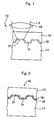
- the optical recording medium 10 is the write-once type medium. As shown in Fig. 1, this medium is composed of a substrate 12, a recording layer 18, and a light transmission layer 20 deposited in this order.
- the recording layer 18 is made of a mixture of a recording assist material and dielectric material.
- data recording/reproducing is performed by a laser beam LB irradiated from the side of the light transmission layer 20.
- the substrate 12 works as a base structure that provides a mechanical rigidity required of the optical recording medium 10.
- Grooves 22 and/or lands 24 are formed on the substrate surface. These grooves 22 and lands 24 work as guide tracks for the laser beam during data recording/reproducing.
- the substrate 12 is about 1.1mm thick and can be made of various materials such as glass, ceramics, and resin.
- Resin is a preferable material in terms of moldability.
- examples of such resin include polycarbonate resin, acryl resin, epoxy resin, polystyrene resin, polyethylene resin, polypropylene resin, silicone resin, fluoride-based resin, ABS resin, and urethane resin.
- polycarbonate resin is preferable in terms of processability.
- the dielectric material contains a state-change material as the base material. Optical characteristics including reflectivity of this material are varied due to energy by laser irradiation or the like.
- the dielectric material as the base material may be any material as long as it can cause a state change. Its principle component can be, for example, oxides, sulfides, nitrides, or their combination. More specifically, its principle component should be at least one dielectric material selected from the group consisting of Al 2 O 3 , AlN, ZnS, GeN, GeCrN, CeO 2 , SiO, SiO 2 , Ta 2 O 5 , SiC, MgO, MgF, LaSiON, Si 3 N 4 , TiO 2 and InSnO. A dielectric material comprising ZnS-SiO 2 as principle components is particularly preferable.
- the thickness of the recording layer 18 is not limited, the thickness is preferably 3-200nm. If it is thinner than 3nm, a sufficient change in the optical characteristics such as reflectivity of the entire layer does not occur even when the base material in the dielectric material has caused a sufficient change of state, and a sufficiently high C/N ratio is not provided. Meanwhile, if the layer is thicker than 200nm, the time for film deposition becomes long and the productivity may decrease, more heat becomes necessary to cause a change in the state of the base material in the dielectric material, and cracks are likely to be produced because of stress in the dielectric material.
- the recording assist material is a material that accelerates the reactions in the base material, and is mixed with the dielectric material as described above.
- the elements of the recording assist material receive the heat of the laser beam and then work on the dielectric material.
- the dielectric material causes a state change in whole or in part (for example, from amorphous to crystalline) to provide recording marks.
- This change of state may accompany a change of state (crystal growth) specific to a material contained in the recording assist material. This change of state will lead to improved C/N.
- the optical behavior against reproducing light significantly differ between the portion where recording marks have been formed and the other portion without recording marks.
- data recording/reproducing can be conducted based on such difference. This state can be confirmed by the X-ray diffraction or transmission electron microscopy.
- the recording assist material has at least one element selected from the group consisting of Sn, Ti, Si, Bi, Ge, C, V, W, Zr, Zn, Mg, Mn, Al, Nb, Au, Cu, Ta and Ag as a principle component.
- the principle component should account for 50% or more in the elements constituting the recording assist material, preferably 80 atomic percent (at%).
- the major element should account for 80 at% or more.
- the light transmission layer 20 is the layer working as the laser beam incident face and as a light path for the laser beam. Its thickness should be 10-300 ⁇ m, more preferably 50-150 ⁇ m.
- the material for the light transmission layer 20 is not limited, but acryl- or epoxy-based ultraviolet-curable resin is preferable. Instead of using an ultraviolet-curable resin film, a transparent sheet made of a transparent resin may be combined with glues and adhesives to form the light transmission layer 20.
- the recording layer 18 is formed on the substrate 12 where grooves 22 and lands 24 have been formed in advance.
- a vapor growth method using chemical species containing elements constituting the second dielectric layer 16B can be adopted.
- Such a vapor growth method may be the vacuum deposition method and sputtering method.
- chemical species where a dielectric material and a recording assist material are mixed may be employed in combination or separately.
- the light transmission layer 20 is formed on the recording layer 18.
- the light transmission layer 20 can be formed by, for example, the spin coating method that uses acryl- or epoxy-based ultraviolet-curable resin of which viscosity has been optimized in advance and cures this resin film by ultraviolet irradiation. Then the manufacturing of the optical recording medium is completed.
- the method of manufacturing the optical recording medium is not limited to the above example, but various techniques for manufacturing well-known optical recording media can be employed as well.
- Laser beam LB of a predetermined output power is irradiated onto the optical recording medium 10.
- the laser beam comes in the light transmission layer 20 and reaches the recording layer 18.
- NA numerical aperture
- the numerical aperture (NA) of the object lens that focuses laser beam LB should be 0.7 or higher, particularly 0.85 or so.
- the wavelength, ⁇ , of laser beam LB should be 450nm or shorter, particularly 405nm or so. Then, it is preferable to make ⁇ /NA ⁇ 640nm.
- the recording assist material constituting the recording layer 18 is heated by laser beam LB and recording assist material work on the adjacent dielectric material, accelerating the state change (for example, change from amorphous to crystalline), to form recording marks therein.
- crystal growth may occur in the recording assist material itself, and the extent of this crystallization may be larger than that of the dielectric material.
- the optical characteristics of the portion where recording marks have been formed are distinctively different from those of the other portion (non-recorded portion). Therefore, when a laser beam for mark reproducing is irradiated onto these recorded portion and the non-recorded portion, their reflectivities differ from each other and thereby the recorded data can be read. In other words, data can be recorded/read through modification of the optical characteristics.
- the recording layer 18 is made of a single layer.
- the present invention is not limited to this structure.
- the state-change assisting layer may be made of two or more layers if the same effect as above can be provided.
- the above optical recording medium 10 does not have a reflection layer on the substrate 12.
- a reflection layer 32 may be formed as in the case of the optical recording medium 30 shown in Fig. 2.
- the reflection layer 32 reflects the laser beam coming in from the side of the light transmission layer 20 and reflects it therethrough. Its thickness should be 5-300nm, preferably 10-200nm.
- the material for the reflection layer 52 is not particularly limited as long as it can reflect laser beams; for example, it can be Mg, Al, Ti, Cr, Fe, Co, Ni, Cu, Zn, Ge, Ag, Pt or Au. Because of high reflectivity, metallic materials such as Al, Au, Ag, or Cu, or their alloys (for example, Ag-Cu alloy) are particularly preferable. If the reflection layer 32 is formed, a high signal restoring ratio (C/N ratio) is easily attained after optical recording by virtue of the multi-interference effect.
- Optical recording media were fabricated via the following steps.
- a polycarbonate substrate of which thickness was 1.1mm and diameter was 120mm was set in a sputtering apparatus.
- a recording layer having a thickness of 10nm was formed by simultaneously sputtering the dielectric material made of a mixture of ZnS and SiO 2 and the recording assist material made of Sn. It was designed to have the recording assist material and ZnS-SiO 2 (80:20) at a molar ratio of 50:50.
- an acrylic ultraviolet-curable resin was coated by the spin coating method and the light transmission layer (thickness: 100 ⁇ m) was formed by ultraviolet irradiation thereon.
- Examples 2 and 3 were prepared in the same manner as in the example 1 except that Sn in the example 1 was replaced by Ag and Ti, respectively.
- an optical recording medium was fabricated to have a single-layered structure where the recording layer was made of only Sn.
- the optical recording medium with a recording layer of a single-layer structure was fabricated without forming any dielectric layer.
- Mg (examples 13-17), Ti (examples 18-25), Sn (examples 26,27), Nb (examples 28-30), or Al (examples 31-34) was mixed in the optical recording medium.
- the optical recording medium with a recording layer of a single-layer structure was fabricated without forming any dielectric layer.
- the recording layer was made of a mixture of Zn and other materials.
- the other materials are ZnS, ZnO and ZnS:SiO 2 (80:20) .
- optical recording media were each set in an optical disk tester (trade name: DDU1000 manufactured by Pulstec Industrial Co., Ltd.).
- a recording laser beam having a wavelength of 405nm (blue) and an object lens with an NA (numerical aperture) of 0.85 were employed in the individual optical recording media in common. This laser beam was focused with a focusing lens installed in the recording head and then irradiated from the light transmission layer side onto the optical recording medium for optical recording.
- the conditions for signal recording were that the modulation mode was (1, 7) RLL, the channel bit length was 0.12 ⁇ m, the linear recording rate was 5.3m/s, the channel clock was 66MHz, and the recorded signals were 8T.
- the information recorded with the aforementioned optical disk tester was reproduced and the C/N ratio of read signals was measured for each of the optical recording media fabricated in the individual examples and compared examples of different recording assist material and dielectric material constituting the recording layer and of different thicknesses of the entire recording layer.
- the wavelength of the laser beam used in reproduction was 405nm
- the NA (numerical aperture) of the object lens was 0.85
- the laser beam output power was 0.3mW.
- Example 1 Example 2 Film structure Recording layer Reflection layer Sn+80:20(10nm) Ag+80:20(10nm) 8T C/N(dB) 51.1 43.4
- Example 3 Compared example 1 Film structure Recording layer Reflection layer Ti+80:20(30nm) Sn(6nm) 8T C/N(dB) 51.2 29.1
- 80:20 means the molar ratio of ZnS:SiO 2 in ZnS+SiO 2 . Notation "ZnS:SiO 2 " is omitted in the table.
- Figure in () indicates the thickness of the entire recording layer.
- Example 4 Film structure Recording layer Reflection layer 80:20+Mg (30nm) 80:20+Nb (50nm) 80:20+Bi (10nm) 8T C/N (dB) 55.7 50.2 51.2
- Example 7 Example 8
- Example 10 Example 11
- Example 12 Film structure Recording layer Reflection layer 80:20+Cu (15nm) 80:20+Ta (20nm) 80:20+Si (40nm) 8T C/N (dB) 49.5 46.6 48.6
- 80:20 means the molar ratio of ZnS:SiO 2 in ZnS+SiO 2 .
- Example 18 Example 19 Example 20 Film structure Recording layer Reflection layer Si3N4+Ti(50nm) ZnS+Ti(30nm) TiO2+Ti(30nm) 8T C/N (dB) 42.3 50.1 48.3 Example 21
- Example 22 Example 23 Film structure Recording layer Reflection layer SiO2+Ti(50nm) SiC+Ti(30nm) 80:20+Ti(10nm) 8T C/N (dB) 44.7 51.6 51.2
- Example 24 Example 25 Film structure Recording layer Reflection layer 50:50+Ti(10nm Ta2O5+Ti(35nm 8T C/N (dB) 45.4 48.5 "80:20” and "50:50” mean the molar ratio of ZnS:SiO 2 in ZnS+SiO 2 .
- ZnS :SiO 2 is omitted in the table.
- Figure in () indicates the thickness of the entire recording layer.
- Table 6 Example 35
- Example 36 Example 37 Film structure Recording layer ZnS+Zn (30nm) ZnO+Zn (30nm) 80:20+Zn (30nm) 8T C/N (dB) 47 48.2 49.5 "80:20” means the molar ratio of ZnS:SiO 2 in ZnS+SiO 2.
- ZnS:SiO 2 is omitted in the table.
- Figure in () indicates the thickness of the entire recording layer.
- the recorded portion and non-recorded portion of the structure of mixture of ZnS-SiO 2 (80:20) and Sn(10nm) was analyzed by the X-ray diffraction. Before recording, crystals of Sn is recognized. After recording, crystals of both of ZnS and Sn observed. And crystallization of ZnS and Sn are recognized with a transmission electron scope.
- the X-ray was Cu-K ⁇ , and the tube voltage and tube current were 50kV and 300mA, respectively.
- the JCPDS cards were used to identify the diffraction peaks. For example, ⁇ -Sn is numbered 04-0673 and the positions of its diffraction peaks are known with reference to the card.
- the optical recording/reproducing method and optical recording medium of the present invention enable to record/read data with a simple structure in a novel manner not adopted in the past while reducing environmental loads.
Landscapes
- Chemical & Material Sciences (AREA)
- Inorganic Chemistry (AREA)
- Optical Record Carriers And Manufacture Thereof (AREA)
- Thermal Transfer Or Thermal Recording In General (AREA)
- Optical Recording Or Reproduction (AREA)
Abstract
Description
- The present invention relates to an optical recording medium and an optical recording/reproducing method using the same.
- As recording media for recording digital data, optical recording media such as CD (Compact Disc) and DVD (Digital Versatile Disc) have been widely used. These optical recording media can be broadly classified into the ROM-type optical recording media such as CD-ROM (Read Only Memory) and DVD-ROM where data is not added or rewritable, the write-once type optical recording media such as CD-R (Recordable) and DVD-R where data can be added but not rewritable, and the rewritable optical recording media such as CD-RW (Rewritable) and DVD-RW where data is rewritable.
- As well known, in the ROM-type optical recording media, data is usually recorded in the form of pre-pits formed on the substrate during manufacturing. In the rewritable optical recording media, phase-change material, for example, is used as a material for the recording layer. In general, data is recorded by the use of a change in the optical characteristics caused by the phase change.
- Meanwhile, in the write-once type optical recording media, organic dyes such as cyanine dyes, phthalocyanine dyes, and azo dyes are used in the recording layer. In general, data is recorded by the use of a change in the optical characteristics caused by its chemical change (occasionally, a physical change may occur along with the chemical change).
- Since organic dyes degrade when exposed to sunlight, for example, it is not easy to improve long-term storage reliability of the medium using such an organic dye in the recording layer thereof. To improve long-term storage reliability of the write-once type optical recording media, it is preferable to make the recording layer with a material other than organic dyes. As an example that has formed the recording layer with a material other than organic dyes, there is a technique to laminate two reaction layers to form a recording layer, as disclosed in Japanese Patent Laid-Open Publication No. Sho 62-204442.
- In recent years, the data recording density has been raised and some next-generation type optical recording media capable of transmitting data at a very high rate have been proposed. In such next-generation optical recording media, the spot size of the laser beam used for recording/reproducing data must be focused small to accomplish a high-capacity, high-speed data transmission rate. In order to make the beam spot smaller, the numerical aperture (NA) of the object lens that focuses the laser beam must be 0.7 or larger, for example, near 0.85, and at the same time the wavelength, λ, of the laser beam must be 450nm or shorter, for example, near 400nm.
- On the other hand, if the NA of the object lens is raised to focus the laser beam, such a problem arises that the tolerance of warpage and tilt of the optical recording medium, namely, the tilt margin becomes very small. The tilt margin, T, can be expressed by the following Equation (1):

- As the Equation (1) indicates, the tilt margin becomes smaller as the NA of the object lens grows. Meanwhile, the coefficient W of wave front aberration is expressed by the following Equation (2):

- As indicated by Equations (1) and (2), the thickness, d, of the light transmission layer (transparent substrate) where the laser beam for data recording/reproducing comes in must be small to effectively prevent coma aberration while ensuring a large tilt margin.
- For these reasons, it is important in the next-generation optical recording media to thin the light transmission layer (transparent substrate) to about 100µm for preventing coma aberration while ensuring a sufficient tilt margin. Thus, in the next-generation type optical recording media, different from the currently-used optical recording media such as CD and DVD, it is difficult to form a recording layer and the like on the light transmission layer (transparent substrate). Instead, such a technique is under investigation that forms a thin resin film as the light transmission layer (transparent substrate) by the spin coating and other methods on the recording layer and the like formed on the substrate. For this purpose, in the manufacturing of the next-generation optical recording media, films are sequentially deposited from the opposite side of the laser incident face, unlike the currently used optical recording media where the films are sequentially deposited from the light incident side.
- However, a problem is found that when the recording layer is made of two reaction layers deposited on the substrate in the next-generation optical recording media the noise level is likely to become high (the C/N ratio becomes small) during signal restoration, compared with the conventional optical recording media such as CD and DVD where the recording layer formed in the light transmission layer (transparent substrate) is made of two reaction layers.
- Meanwhile, to meet the recent growing needs for environmental protection, the recording layer of the optical recording medium should be made of materials of a smaller environmental burden. Furthermore, to improve the long-term storage reliability, the material for the recording layer of an optical recording medium should be sufficiently resistant to corrosion and degradation.
- An object of the present invention is to provide a novel optical recording/reproducing method and an optical recording medium particularly useful to the recording/reproducing systems adopting next-generation type optical recording media.
- As a result of an intensive study, the inventor has found that a simple film structure using environmentally friendly materials such as Sn and ZnS can provide excellent optical recording/reproducing characteristics.
- Specifically, the above object is achieved by the following method and medium.
- (1) An optical recording/reproducing method comprising the steps of:
- externally irradiating a laser beam of which intensity is modulated in accordance with information to be recorded onto a recording layer formed on a substrate and made of a mixture of at least a recording assist material and a dielectric material, and thereby changing a state of at least a part of the dielectric material and changing optical characteristics thereof to record the information; and
- reading a change in reflectivity resulting from the change in optical characteristics to reproduce the information.
- (2) An optical recording/reproducing method comprising the steps of:
- externally irradiating a laser beam of which intensity is modulated in accordance with information to be recorded onto a recording layer formed on a substrate and made of a mixture of at least a recording assist material and a dielectric material, and thereby changing a state of at least a part of the recording assist material and thereby changing optical characteristics thereof to record the information; and
- reading a change in reflectivity resulting from the change in optical characteristics to reproduce the information.
- (3) An optical recording/reproducing method comprising the steps of:
- externally irradiating a laser beam of which intensity is modulated in accordance with information to be recorded onto a recording layer formed on a substrate and made of a mixture of at least a recording assist material and a dielectric material, and thereby changing a state of at least a part of the dielectric material and a state of at least a part of the recording assist material and changing optical characteristics thereof to record the information; and
- reading a change in reflectivity resulting from the change in optical characteristics to reproduce the information.
- (4) The optical recording/reproducing method according to any one of (1), (2), and (3), wherein the state change of at least one of the dielectric material and the recording assist material is crystal growth.
- (5) An optical recording medium comprising:
- a substrate; and
- at least a recording layer formed on the substrate and made of a mixture of a recording assist material and a dielectric material, wherein
- a laser beam of which intensity is modulated in accordance with information to be recorded is externally irradiated onto the recording layer to cause a state change in at least a part of the recording assist material to record the information by a change in optical characteristics thereof, and the information can be reproduced by reading a change in reflectivity resulting from the change in optical characteristics.
- (6) An optical recording medium comprising:
- a substrate; and
- at least a recording layer formed on the substrate and made of a mixture of a recording assist material including a state-change assisting material and a dielectric material including a base material of which state can be changed, wherein
- a laser beam of which intensity is modulated in accordance with information to be recorded is externally irradiated onto the recording layer to cause a state change in at least a part of the base material to record the information by a change in optical characteristics thereof, and
- the information can be reproduced by reading a change in reflectivity resulting from the change in optical characteristics.
- (7) An optical recording medium comprising:
- a substrate; and
- at least a recording layer formed on the substrate and made of a mixture of a recording assist material including a state-change assisting material and a dielectric material including a base material of which state can be changed, wherein
- a laser beam of which intensity is modulated in accordance with information to be recorded is externally irradiated onto the recording layer to cause a state change in at least a part of the recording assist material and in at least a part of the dielectric material to record the information by a change in optical characteristics thereof, and
- the information can be reproduced by reading a change in reflectivity resulting from the change in optical characteristics.
- (8) An optical recording medium comprising:
- a substrate; and
- at least a recording layer formed on the substrate and made of a mixture of a recording assist material and a dielectric material, wherein
- the recording assist material includes at least one element selected from the group consisting of Sn, Ti, Si, Bi, Ge, C, V, W, Zr, Zn, Mg, Mn, Ag, Al, Nb, Au, Cu, and Ta, as a principle component.
- (9) The optical recording medium according to (8), wherein the dielectric material has at least one material selected from the group consisting of Al2O3, AlN, ZnO, ZnS, GeN, GeCrN, CeO2, SiO, SiO2, Ta2O5, SiC, MgO, MgF, LaSiON, Si3N4, TiO2, and InSnO, as a principle component.
- Fig. 1 is a schematic view showing an optical recording medium according to a first embodiment of the invention;
- Fig. 2 is a schematic view showing an optical recording medium according to a second embodiment of the invention;
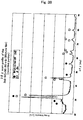
- Fig. 3A is an X-ray diffraction pattern of a non-recorded portion of the optical recording medium of the example 1; and
- Fig. 3B is an X-ray diffraction pattern of a recorded portion of the optical recording medium of the example 1.
- Now embodiments of the invention will be described in detail with reference to the accompanying drawings.
- The
optical recording medium 10 according to the present embodiments is the write-once type medium. As shown in Fig. 1, this medium is composed of asubstrate 12, arecording layer 18, and alight transmission layer 20 deposited in this order. Therecording layer 18 is made of a mixture of a recording assist material and dielectric material. In theoptical recording medium 10 of this structure, data recording/reproducing is performed by a laser beam LB irradiated from the side of thelight transmission layer 20. - The
substrate 12 works as a base structure that provides a mechanical rigidity required of theoptical recording medium 10.Grooves 22 and/or lands 24 are formed on the substrate surface. Thesegrooves 22 and lands 24 work as guide tracks for the laser beam during data recording/reproducing. - The
substrate 12 is about 1.1mm thick and can be made of various materials such as glass, ceramics, and resin. Resin is a preferable material in terms of moldability. Examples of such resin include polycarbonate resin, acryl resin, epoxy resin, polystyrene resin, polyethylene resin, polypropylene resin, silicone resin, fluoride-based resin, ABS resin, and urethane resin. Particularly, polycarbonate resin is preferable in terms of processability. - The dielectric material contains a state-change material as the base material. Optical characteristics including reflectivity of this material are varied due to energy by laser irradiation or the like.
- The dielectric material as the base material may be any material as long as it can cause a state change. Its principle component can be, for example, oxides, sulfides, nitrides, or their combination. More specifically, its principle component should be at least one dielectric material selected from the group consisting of Al2O3, AlN, ZnS, GeN, GeCrN, CeO2, SiO, SiO2, Ta2O5, SiC, MgO, MgF, LaSiON, Si3N4, TiO2 and InSnO. A dielectric material comprising ZnS-SiO2 as principle components is particularly preferable.
- Note that the "use of a . . . material as a principle component" means that the content of such a dielectric material is the largest in the base material. Also note that "ZnS-SiO2" means a mixture of ZnS and SiO2.
- The thickness of the
recording layer 18 is not limited, the thickness is preferably 3-200nm. If it is thinner than 3nm, a sufficient change in the optical characteristics such as reflectivity of the entire layer does not occur even when the base material in the dielectric material has caused a sufficient change of state, and a sufficiently high C/N ratio is not provided. Meanwhile, if the layer is thicker than 200nm, the time for film deposition becomes long and the productivity may decrease, more heat becomes necessary to cause a change in the state of the base material in the dielectric material, and cracks are likely to be produced because of stress in the dielectric material. - The recording assist material is a material that accelerates the reactions in the base material, and is mixed with the dielectric material as described above. When a laser beam of a power higher than a predetermined level is irradiated thereon, the elements of the recording assist material receive the heat of the laser beam and then work on the dielectric material. Then the dielectric material causes a state change in whole or in part (for example, from amorphous to crystalline) to provide recording marks. This change of state may accompany a change of state (crystal growth) specific to a material contained in the recording assist material. This change of state will lead to improved C/N.
- In the
recording layer 18, the optical behavior against reproducing light significantly differ between the portion where recording marks have been formed and the other portion without recording marks. Thus data recording/reproducing can be conducted based on such difference. This state can be confirmed by the X-ray diffraction or transmission electron microscopy. - The recording assist material has at least one element selected from the group consisting of Sn, Ti, Si, Bi, Ge, C, V, W, Zr, Zn, Mg, Mn, Al, Nb, Au, Cu, Ta and Ag as a principle component.
- The principle component should account for 50% or more in the elements constituting the recording assist material, preferably 80 atomic percent (at%).
- If it is lower than 50 at%, the effect of changing the state of the dielectric material becomes insufficient and then C/N decreases. Furthermore, because of recording, the film itself is likely to be destructed and thereby storage reliability degrades.
- Meanwhile, to lower the laser beam power to some extent for a smooth state change in the dielectric layer, the major element should account for 80 at% or more.
- The
light transmission layer 20 is the layer working as the laser beam incident face and as a light path for the laser beam. Its thickness should be 10-300µm, more preferably 50-150µm. The material for thelight transmission layer 20 is not limited, but acryl- or epoxy-based ultraviolet-curable resin is preferable. Instead of using an ultraviolet-curable resin film, a transparent sheet made of a transparent resin may be combined with glues and adhesives to form thelight transmission layer 20. - Next explained is an example of how to manufacture the
optical recording medium 10. - First, the
recording layer 18 is formed on thesubstrate 12 wheregrooves 22 and lands 24 have been formed in advance. For the deposition of the dielectric material and the recording assist material, a vapor growth method using chemical species containing elements constituting the second dielectric layer 16B can be adopted. Such a vapor growth method may be the vacuum deposition method and sputtering method. In this case, chemical species where a dielectric material and a recording assist material are mixed may be employed in combination or separately. - Finally, the
light transmission layer 20 is formed on therecording layer 18. Thelight transmission layer 20 can be formed by, for example, the spin coating method that uses acryl- or epoxy-based ultraviolet-curable resin of which viscosity has been optimized in advance and cures this resin film by ultraviolet irradiation. Then the manufacturing of the optical recording medium is completed. - The method of manufacturing the optical recording medium is not limited to the above example, but various techniques for manufacturing well-known optical recording media can be employed as well.
- Now the optical recording/reproducing method using the above
optical recording medium 10 will be described below. - Laser beam LB of a predetermined output power is irradiated onto the
optical recording medium 10. The laser beam comes in thelight transmission layer 20 and reaches therecording layer 18. It is preferred that the numerical aperture (NA) of the object lens that focuses laser beam LB should be 0.7 or higher, particularly 0.85 or so. It is preferred that the wavelength, λ, of laser beam LB should be 450nm or shorter, particularly 405nm or so. Then, it is preferable to make λ/NA < 640nm. - By irradiation of laser beam LB, the recording assist material constituting the
recording layer 18 is heated by laser beam LB and recording assist material work on the adjacent dielectric material, accelerating the state change (for example, change from amorphous to crystalline), to form recording marks therein. - In this case, crystal growth may occur in the recording assist material itself, and the extent of this crystallization may be larger than that of the dielectric material.
- The optical characteristics of the portion where recording marks have been formed are distinctively different from those of the other portion (non-recorded portion). Therefore, when a laser beam for mark reproducing is irradiated onto these recorded portion and the non-recorded portion, their reflectivities differ from each other and thereby the recorded data can be read. In other words, data can be recorded/read through modification of the optical characteristics.
- The present invention is not limited to the above embodiment and can be modified in various ways within the scope of the appended claims, and such modifications are also included in the present invention.
- In the
optical recording medium 10 according to the above embodiments, therecording layer 18 is made of a single layer. The present invention, however, is not limited to this structure. The state-change assisting layer may be made of two or more layers if the same effect as above can be provided. - The above
optical recording medium 10 does not have a reflection layer on thesubstrate 12. However, to enhance the laser reflection from the recorded portion having recording marks and the non-recorded portion, areflection layer 32 may be formed as in the case of theoptical recording medium 30 shown in Fig. 2. - The
reflection layer 32 reflects the laser beam coming in from the side of thelight transmission layer 20 and reflects it therethrough. Its thickness should be 5-300nm, preferably 10-200nm. The material for the reflection layer 52 is not particularly limited as long as it can reflect laser beams; for example, it can be Mg, Al, Ti, Cr, Fe, Co, Ni, Cu, Zn, Ge, Ag, Pt or Au. Because of high reflectivity, metallic materials such as Al, Au, Ag, or Cu, or their alloys (for example, Ag-Cu alloy) are particularly preferable. If thereflection layer 32 is formed, a high signal restoring ratio (C/N ratio) is easily attained after optical recording by virtue of the multi-interference effect. - Now the present invention will be explained more specifically along with some examples, but the invention is not limited to those examples.
- Optical recording media were fabricated via the following steps.
- First, a polycarbonate substrate of which thickness was 1.1mm and diameter was 120mm was set in a sputtering apparatus. On the light reflection layer of this polycarbonate substrate, a recording layer having a thickness of 10nm was formed by simultaneously sputtering the dielectric material made of a mixture of ZnS and SiO2 and the recording assist material made of Sn. It was designed to have the recording assist material and ZnS-SiO2(80:20) at a molar ratio of 50:50.
- Next, on the recording layer, an acrylic ultraviolet-curable resin was coated by the spin coating method and the light transmission layer (thickness: 100µm) was formed by ultraviolet irradiation thereon.
- The molar ratio between ZnS and SiO2 in the first and second dielectric layers was ZnS:SiO2 = 80:20.
- Examples 2 and 3 were prepared in the same manner as in the example 1 except that Sn in the example 1 was replaced by Ag and Ti, respectively.
- In the compared example, an optical recording medium was fabricated to have a single-layered structure where the recording layer was made of only Sn.
- The optical recording medium with a recording layer of a single-layer structure was fabricated without forming any dielectric layer. The recording layer was made of a mixture of ZnS-SiO2 (ZnS:SiO2 = 80:20) and a metal or semi-metal of Mg, Nb, Bi, Mg, Au, Al, Au, Cu, Ta, or Si.
- The optical recording media were fabricated by replacing ZnS-SiO2 (ZnS:SiO2=80:20) employed in the examples 4-12 to other materials. Mg (examples 13-17), Ti (examples 18-25), Sn (examples 26,27), Nb (examples 28-30), or Al (examples 31-34) was mixed in the optical recording medium.
- The optical recording medium with a recording layer of a single-layer structure was fabricated without forming any dielectric layer. The recording layer was made of a mixture of Zn and other materials. The other materials are ZnS, ZnO and ZnS:SiO2(80:20) .
- The above fabricated optical recording media were each set in an optical disk tester (trade name: DDU1000 manufactured by Pulstec Industrial Co., Ltd.). A recording laser beam having a wavelength of 405nm (blue) and an object lens with an NA (numerical aperture) of 0.85 were employed in the individual optical recording media in common. This laser beam was focused with a focusing lens installed in the recording head and then irradiated from the light transmission layer side onto the optical recording medium for optical recording.
- The conditions for signal recording were that the modulation mode was (1, 7) RLL, the channel bit length was 0.12µm, the linear recording rate was 5.3m/s, the channel clock was 66MHz, and the recorded signals were 8T.
- Next, the information recorded with the aforementioned optical disk tester was reproduced and the C/N ratio of read signals was measured for each of the optical recording media fabricated in the individual examples and compared examples of different recording assist material and dielectric material constituting the recording layer and of different thicknesses of the entire recording layer. In the reproducing apparatus, the wavelength of the laser beam used in reproduction was 405nm, the NA (numerical aperture) of the object lens was 0.85, and the laser beam output power was 0.3mW.
- The test results are listed in Tables 1-6.
Table 1 Example 1 Example 2 Film structure Recording layer Reflection layer Sn+80:20(10nm) Ag+80:20(10nm) 8T C/N(dB) 51.1 43.4 Example 3 Compared example 1 Film structure Recording layer Reflection layer Ti+80:20(30nm) Sn(6nm) 8T C/N(dB) 51.2 29.1 "80:20"means the molar ratio of ZnS:SiO2 in ZnS+SiO2. Notation "ZnS:SiO2" is omitted in the table. Figure in () indicates the thickness of the entire recording layer. Table 2 Example 4 Example 5 Example 6 Film structure Recording layer Reflection layer 80:20+Mg (30nm) 80:20+Nb (50nm) 80:20+Bi (10nm) 8T C/N (dB) 55.7 50.2 51.2 Example 7 Example 8 Example 9 Film structure Recording layer Reflection layer 80:20+MgAu (30nm) 80:20+Al (15nm) 80:20+Au (20nm) 8T C/N (dB) 52.8 55.4 48.9 Example 10 Example 11 Example 12 Film structure Recording layer Reflection layer 80:20+Cu (15nm) 80:20+Ta (20nm) 80:20+Si (40nm) 8T C/N (dB) 49.5 46.6 48.6 "80:20" means the molar ratio of ZnS:SiO2 in ZnS+SiO2. Notation "ZnS:SiO2" is omitted in the table. Figure in () indicated the thickness of the entire recording layer. Table 3 Example 13 Example 14 Example 15 Film structure Recording layer Reflection layer MgO+Mg(30nm) MgF+Mg(30nm) SiO2+Mg (20nm) 8T C/N (dB) 35.1 48.2 55.4 Example 16 Example 17 Film structure Recording layer Reflection layer ZnS+Mg (20nm) LaSiON+Mg(15nm) 8T C/N (dB) 52 52.3 Figure in () indicates the thickness of the entire recording layer. Table 4 Example 18 Example 19 Example 20 Film structure Recording layer Reflection layer Si3N4+Ti(50nm) ZnS+Ti(30nm) TiO2+Ti(30nm) 8T C/N (dB) 42.3 50.1 48.3 Example 21 Example 22 Example 23 Film structure Recording layer Reflection layer SiO2+Ti(50nm) SiC+Ti(30nm) 80:20+Ti(10nm) 8T C/N (dB) 44.7 51.6 51.2 Example 24 Example 25 Film structure Recording layer Reflection layer 50:50+Ti(10nm Ta2O5+Ti(35nm 8T C/N (dB) 45.4 48.5 "80:20" and "50:50" mean the molar ratio of ZnS:SiO2 in ZnS+SiO2. Notation "ZnS : SiO2" is omitted in the table. Figure in () indicates the thickness of the entire recording layer. Table 5 Example 26 Example 27 Example 28 Film structure InSnO+Sn(50nm) 80:20+Sn(10nm) 80:20+Nb(50nm) Recording layer Reflection layer 8T C/N (dB) 40.9 32.1 50.2 Example 29 Example 30 Example 31 Film structure Recording layer Reflection layer Ta2O5+Nb(25nm) TiO2+Nb(35nm) 80:20+Al(15nm) 8T C/N (dB) 45.4 54.6 55.4 Example 32 Example 33 Example 34 Film structure Recording layer Reflection layer LaSiON+Al(40nm) Ta205+Al(25nm) TiO2+Al (35nm) 8T C/N (dB) 49.3 50.5 48.9 "80:20" means the molar ratio of ZnS:SiO2 in ZnS+SiO2. Notation "ZnS :SiO2" is omitted in the table. Figure in () indicates the thickness of the entire recording layer. Table 6 Example 35 Example 36 Example 37 Film structure Recording layer ZnS+Zn (30nm) ZnO+Zn (30nm) 80:20+Zn (30nm) 8T C/N (dB) 47 48.2 49.5 "80:20" means the molar ratio of ZnS:SiO2 in ZnS+SiO2. Notation "ZnS:SiO2" is omitted in the table. Figure in () indicates the thickness of the entire recording layer. - As evident from the results shown in Tables 1-6, these examples 1-37 have succeeded in providing a high C/N ratio by mixing the dielectric material and the recording assist material for recording.
- The recorded portion and non-recorded portion of the structure of mixture of ZnS-SiO2(80:20) and Sn(10nm) was analyzed by the X-ray diffraction. Before recording, crystals of Sn is recognized. After recording, crystals of both of ZnS and Sn observed. And crystallization of ZnS and Sn are recognized with a transmission electron scope.
- In this measurement of X-ray diffraction, the X-ray was Cu-Kα, and the tube voltage and tube current were 50kV and 300mA, respectively. The JCPDS cards were used to identify the diffraction peaks. For example, β-Sn is numbered 04-0673 and the positions of its diffraction peaks are known with reference to the card.
- Under the structure described in the example 1 (ZnS-SiO2/Sn mixed type layered structure), the recorded portion and the non-recorded portion were analyzed by the X-ray diffraction (Figs. 3A and 3B).
- A diffraction peak of β-Sn is observed in the diffraction pattern of the non-recorded portion (Fig. 3A) , while almost no peak of ZnS was observed. Thus it is understood that this Sn is crystalline. On the other hand, the recorded portion (Fig. 3B) showed a sharp diffraction peak of ZnS, indicating crystallization of ZnS. A number of ZnS diffraction peaks indicated that the crystallization of ZnS proceeds by recording.
- As described above, the optical recording/reproducing method and optical recording medium of the present invention enable to record/read data with a simple structure in a novel manner not adopted in the past while reducing environmental loads.
Claims (9)
- An optical recording/reproducing method comprising the steps of:externally irradiating a laser beam of which intensity is modulated in accordance with information to be recorded onto a recording layer(18) formed on a substrate(12) and made of a mixture of at least a recording assist material and a dielectric material, and thereby changing a state of at least a part of the dielectric material and changing optical characteristics thereof to record the information; andreading a change in reflectivity resulting from the change in optical characteristics to reproduce the information.
- An optical recording/reproducing method comprising the steps of:externally irradiating a laser beam of which intensity is modulated in accordance with information to be recorded onto a recording layer(18) formed on a substrate(12) and made of a mixture of at least a recording assist material and a dielectric material, and thereby changing a state of at least a part of the recording assist material and thereby changing optical characteristics thereof to record the information; andreading a change in reflectivity resulting from the change in optical characteristics to reproduce the information.
- An optical recording/reproducing method comprising the steps of:externally irradiating a laser beam of which intensity is modulated in accordance with information to be recorded onto a recording layer(18) formed on a substrate(12) and made of a mixture of at least a recording assist material and a dielectric material, and thereby changing a state of at least a part of the dielectric material and a state of at least a part of the recording assist material and changing optical characteristics thereof to record the information; andreading a change in reflectivity resulting from the change in optical characteristics to reproduce the information.
- The optical recording/reproducing method according to claim 1, 2 or 3, wherein the state change of at least one of the dielectric material and the recording assist material is crystal growth.
- An optical recording medium(10,30) comprising:a substrate(12); andat least a recording layer(18) formed on the substrate(12) and made of a mixture of a recording assist material and a dielectric material, whereina laser beam of which intensity is modulated in accordance with information to be recorded is externally irradiated onto the recording layer(18) to cause a state change in at least a part of the recording assist material to record the information by a change in optical characteristics thereof, andthe information can be reproduced by reading a change in reflectivity resulting from the change in optical characteristics.
- An optical recording medium (10, 30) comprising:a substrate(12); andat least a recording layer(18) formed on the substrate(12) andmade of a mixture of a recording assist material including a state-change assisting material and a dielectric material including a base material of which state can be changed,wherein
a laser beam of which intensity is modulated in accordance with information to be recorded is externally irradiated onto the recording layer(18) to cause a state change in at least a part of the base material to record the information by a change in optical characteristics thereof, and
the information can be reproduced by reading a change in reflectivity resulting from the change in optical characteristics. - An optical recording medium(10,30) comprising:a substrate(12); andat least a recording layer(18) formed on the substrate(12) and made of a mixture of a recording assist material including a state-change assisting material and a dielectric material including a base material of which state can be changed,wherein
a laser beam of which intensity is modulated in accordance with information to be recorded is externally irradiated onto the recording layer(18) to cause a state change in at least a part of the recording assist material and in at least a part of the dielectric material to record the information by a change in optical characteristics thereof, and the information can be reproduced by reading a change in reflectivity resulting from the change in optical characteristics. - An optical recording medium(10,30) comprising:a substrate(12); andat least a recording layer(18) formed on the substrate(18) and made of a mixture of a recording assist material and a dielectric material, whereinthe recording assist material includes at least one element selected from the group consisting of Sn, Ti, Si, Bi, Ge, C, V, W, Zr, Zn, Mg, Mn, Ag, Al, Nb, Au, Cu, and Ta, as a principle component.
- The optical recording medium(10,30) according to claim 8, wherein the dielectric material has at least one material selected from the group consisting of Al2O3, AlN, ZnO, ZnS, GeN, GeCrN, CeO2, SiO, SiO2, Ta2O5, SiC, MgO, MgF, LaSiON, Si3N4, TiO2, and InSnO, as a principle component.
Applications Claiming Priority (4)
| Application Number | Priority Date | Filing Date | Title |
|---|---|---|---|
| JP2002162116 | 2002-06-03 | ||
| JP2002162116 | 2002-06-03 | ||
| JP2003035067 | 2003-02-13 | ||
| JP2003035067 | 2003-02-13 |
Publications (2)
| Publication Number | Publication Date |
|---|---|
| EP1403857A2 true EP1403857A2 (en) | 2004-03-31 |
| EP1403857A3 EP1403857A3 (en) | 2007-03-07 |
Family
ID=29738317
Family Applications (1)
| Application Number | Title | Priority Date | Filing Date |
|---|---|---|---|
| EP03012150A Withdrawn EP1403857A3 (en) | 2002-06-03 | 2003-06-02 | Optical recording/reproducing method and optical recording medium |
Country Status (6)
| Country | Link |
|---|---|
| US (1) | US7136343B2 (en) |
| EP (1) | EP1403857A3 (en) |
| JP (1) | JP2004296056A (en) |
| KR (1) | KR100678301B1 (en) |
| CN (1) | CN1469362A (en) |
| TW (1) | TWI256629B (en) |
Families Citing this family (8)
| Publication number | Priority date | Publication date | Assignee | Title |
|---|---|---|---|---|
| US7235501B2 (en) | 2004-12-13 | 2007-06-26 | Micron Technology, Inc. | Lanthanum hafnium oxide dielectrics |
| US7560395B2 (en) | 2005-01-05 | 2009-07-14 | Micron Technology, Inc. | Atomic layer deposited hafnium tantalum oxide dielectrics |
| US7972974B2 (en) | 2006-01-10 | 2011-07-05 | Micron Technology, Inc. | Gallium lanthanide oxide films |
| US7605030B2 (en) | 2006-08-31 | 2009-10-20 | Micron Technology, Inc. | Hafnium tantalum oxynitride high-k dielectric and metal gates |
| US7544604B2 (en) | 2006-08-31 | 2009-06-09 | Micron Technology, Inc. | Tantalum lanthanide oxynitride films |
| US7776765B2 (en) | 2006-08-31 | 2010-08-17 | Micron Technology, Inc. | Tantalum silicon oxynitride high-k dielectrics and metal gates |
| US7759747B2 (en) | 2006-08-31 | 2010-07-20 | Micron Technology, Inc. | Tantalum aluminum oxynitride high-κ dielectric |
| US7563730B2 (en) | 2006-08-31 | 2009-07-21 | Micron Technology, Inc. | Hafnium lanthanide oxynitride films |
Citations (3)
| Publication number | Priority date | Publication date | Assignee | Title |
|---|---|---|---|---|
| US4499178A (en) * | 1981-06-12 | 1985-02-12 | Fuji Photo Film Co., Ltd. | Optical information recording material |
| EP0173523A2 (en) * | 1984-08-24 | 1986-03-05 | Kabushiki Kaisha Toshiba | Optical memory |
| US5635267A (en) * | 1992-09-17 | 1997-06-03 | Matsushita Electric Industrial Co., Ltd. | Optical information recording medium of phase change type having variably grooved tracks depending on their radial locations |
Family Cites Families (2)
| Publication number | Priority date | Publication date | Assignee | Title |
|---|---|---|---|---|
| JPS62204442A (en) | 1986-03-03 | 1987-09-09 | Toshiba Corp | Optical recording medium and its recording method |
| TW484126B (en) * | 1999-03-26 | 2002-04-21 | Matsushita Electric Ind Co Ltd | Manufacturing and recording regeneration method for information record medium |
-
2003
- 2003-05-20 TW TW092113636A patent/TWI256629B/en not_active IP Right Cessation
- 2003-05-29 US US10/447,109 patent/US7136343B2/en active Active
- 2003-05-30 KR KR1020030034739A patent/KR100678301B1/en active IP Right Grant
- 2003-06-02 EP EP03012150A patent/EP1403857A3/en not_active Withdrawn
- 2003-06-02 JP JP2003156562A patent/JP2004296056A/en active Pending
- 2003-06-03 CN CNA031379958A patent/CN1469362A/en active Pending
Patent Citations (3)
| Publication number | Priority date | Publication date | Assignee | Title |
|---|---|---|---|---|
| US4499178A (en) * | 1981-06-12 | 1985-02-12 | Fuji Photo Film Co., Ltd. | Optical information recording material |
| EP0173523A2 (en) * | 1984-08-24 | 1986-03-05 | Kabushiki Kaisha Toshiba | Optical memory |
| US5635267A (en) * | 1992-09-17 | 1997-06-03 | Matsushita Electric Industrial Co., Ltd. | Optical information recording medium of phase change type having variably grooved tracks depending on their radial locations |
Also Published As
| Publication number | Publication date |
|---|---|
| JP2004296056A (en) | 2004-10-21 |
| US7136343B2 (en) | 2006-11-14 |
| CN1469362A (en) | 2004-01-21 |
| TW200307925A (en) | 2003-12-16 |
| TWI256629B (en) | 2006-06-11 |
| KR100678301B1 (en) | 2007-02-01 |
| EP1403857A3 (en) | 2007-03-07 |
| US20030235134A1 (en) | 2003-12-25 |
| KR20030094051A (en) | 2003-12-11 |
Similar Documents
| Publication | Publication Date | Title |
|---|---|---|
| US20070190460A1 (en) | Optical recording/reproducing method | |
| US7601481B2 (en) | Multilayer phase-change information recording medium, and method for recording and reproducing using the same | |
| US20040157158A1 (en) | Optical recording medium | |
| US6929840B2 (en) | Optical recording medium, method for manufacturing the same and target used for sputtering process | |
| KR100734641B1 (en) | Optical Recording Medium, Optical Recording/Reproducing Apparatus, Optical Recording Apparatus and Optical Reproducing Apparatus, Data Recording/Reproducing Method for Optical Recording Medium, and Data Recording Method and Data Reproducing Method | |
| US20040191685A1 (en) | Optical recording medium | |
| KR20040063839A (en) | Optical recording medium | |
| EP1398767B1 (en) | Optical recording/reproducing method and optical recording medium | |
| EP1403857A2 (en) | Optical recording/reproducing method and optical recording medium | |
| CN101512647B (en) | Multi-layered phase-change optical recording medium | |
| JPWO2004032130A1 (en) | Optical information recording medium and manufacturing method thereof | |
| JP4251142B2 (en) | Write-once optical recording medium | |
| EP1400960A2 (en) | Optical recording/reproducing method and optical recording medium | |
| JP5298623B2 (en) | Write-once optical recording medium | |
| EP1922728B1 (en) | Multilayer optical recording medium and optical recording method | |
| JP2007141417A (en) | Write-once type optical recording medium and its manufacturing method | |
| JP2005243218A (en) | Optical recording medium | |
| JP4232159B2 (en) | Optical recording medium | |
| US20060165944A1 (en) | Optical recording medium | |
| JP2005267797A (en) | Optical information recording medium, method for manufacturing same, and sputtering target | |
| JP2004342196A (en) | Write-once optical recording medium and its recording method | |
| JP2004296057A (en) | Optical recording and reproducing method and optical recording medium | |
| JP2005203072A (en) | Optical recording medium |
Legal Events
| Date | Code | Title | Description |
|---|---|---|---|
| PUAI | Public reference made under article 153(3) epc to a published international application that has entered the european phase |
Free format text: ORIGINAL CODE: 0009012 |
|
| AK | Designated contracting states |
Kind code of ref document: A2 Designated state(s): AT BE BG CH CY CZ DE DK EE ES FI FR GB GR HU IE IT LI LU MC NL PT RO SE SI SK TR |
|
| AX | Request for extension of the european patent |
Extension state: AL LT LV MK |
|
| PUAL | Search report despatched |
Free format text: ORIGINAL CODE: 0009013 |
|
| STAA | Information on the status of an ep patent application or granted ep patent |
Free format text: STATUS: THE APPLICATION HAS BEEN WITHDRAWN |
|
| AK | Designated contracting states |
Kind code of ref document: A3 Designated state(s): AT BE BG CH CY CZ DE DK EE ES FI FR GB GR HU IE IT LI LU MC NL PT RO SE SI SK TR |
|
| AX | Request for extension of the european patent |
Extension state: AL LT LV MK |
|
| 18W | Application withdrawn |
Effective date: 20070209 |