EP1403840A1 - Arithmetic device and encryption/decryption device - Google Patents
Arithmetic device and encryption/decryption device Download PDFInfo
- Publication number
- EP1403840A1 EP1403840A1 EP03720936A EP03720936A EP1403840A1 EP 1403840 A1 EP1403840 A1 EP 1403840A1 EP 03720936 A EP03720936 A EP 03720936A EP 03720936 A EP03720936 A EP 03720936A EP 1403840 A1 EP1403840 A1 EP 1403840A1
- Authority
- EP
- European Patent Office
- Prior art keywords
- data
- calculation
- input
- latch
- outputted
- Prior art date
- Legal status (The legal status is an assumption and is not a legal conclusion. Google has not performed a legal analysis and makes no representation as to the accuracy of the status listed.)
- Granted
Links
Images

Classifications
-
- H—ELECTRICITY
- H04—ELECTRIC COMMUNICATION TECHNIQUE
- H04L—TRANSMISSION OF DIGITAL INFORMATION, e.g. TELEGRAPHIC COMMUNICATION
- H04L9/00—Cryptographic mechanisms or cryptographic arrangements for secret or secure communications; Network security protocols
- H04L9/06—Cryptographic mechanisms or cryptographic arrangements for secret or secure communications; Network security protocols the encryption apparatus using shift registers or memories for block-wise or stream coding, e.g. DES systems or RC4; Hash functions; Pseudorandom sequence generators
-
- H—ELECTRICITY
- H04—ELECTRIC COMMUNICATION TECHNIQUE
- H04L—TRANSMISSION OF DIGITAL INFORMATION, e.g. TELEGRAPHIC COMMUNICATION
- H04L9/00—Cryptographic mechanisms or cryptographic arrangements for secret or secure communications; Network security protocols
- H04L9/002—Countermeasures against attacks on cryptographic mechanisms
- H04L9/003—Countermeasures against attacks on cryptographic mechanisms for power analysis, e.g. differential power analysis [DPA] or simple power analysis [SPA]
-
- G—PHYSICS
- G09—EDUCATION; CRYPTOGRAPHY; DISPLAY; ADVERTISING; SEALS
- G09C—CIPHERING OR DECIPHERING APPARATUS FOR CRYPTOGRAPHIC OR OTHER PURPOSES INVOLVING THE NEED FOR SECRECY
- G09C1/00—Apparatus or methods whereby a given sequence of signs, e.g. an intelligible text, is transformed into an unintelligible sequence of signs by transposing the signs or groups of signs or by replacing them by others according to a predetermined system
-
- H—ELECTRICITY
- H04—ELECTRIC COMMUNICATION TECHNIQUE
- H04L—TRANSMISSION OF DIGITAL INFORMATION, e.g. TELEGRAPHIC COMMUNICATION
- H04L9/00—Cryptographic mechanisms or cryptographic arrangements for secret or secure communications; Network security protocols
- H04L9/06—Cryptographic mechanisms or cryptographic arrangements for secret or secure communications; Network security protocols the encryption apparatus using shift registers or memories for block-wise or stream coding, e.g. DES systems or RC4; Hash functions; Pseudorandom sequence generators
- H04L9/0618—Block ciphers, i.e. encrypting groups of characters of a plain text message using fixed encryption transformation
- H04L9/0625—Block ciphers, i.e. encrypting groups of characters of a plain text message using fixed encryption transformation with splitting of the data block into left and right halves, e.g. Feistel based algorithms, DES, FEAL, IDEA or KASUMI
Definitions
- the present invention relates to a data calculating device and a data encryptor/decryptor for calculation of data to encrypt and/or decrypt the data.
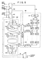
- a device shown in Fig. 5 is contrived as an encryptor/decryptor conforming with an encryption algorithm of DES (Data Encryption Standard).
- DES Data Encryption Standard
- Key data secret key
- input data plain text data or encrypted text data
- a mode signal indicative of encryption or decryption is latched in a latch circuit 83 according to the clock CLK.
- the key data outputted from the latch circuit 81 are supplied to a key generator 90, and the key data K1 to K16 of 16 stages each composed of 48 bits are outputted sequentially from the key generator 90.
- the 64-bit key data outputted from the latch circuit 81 are converted into 56-bit key data in a conversion circuit 91, and higher-order 28-bit data and lower-order 28-bit data are shifted by 1 bit or 2 bits in shift circuits 93 and 94, and then are combined together to form 56-bit key data, which are converted into 48-bit key data in a conversion circuit 95, whereby first-stage key data are generated.
- the output data (plain text data or encrypted text data) from the latch circuit 82 are supplied to a calculator 100, where the following calculation is executed.
- the 64-bit data outputted from the latch circuit 82 are transposed bit by bit in an initial transposition circuit 101, and the lower-order 32 bits out of the entire 64-bit data obtained after such initial transposition and the key data K1 are calculated together in a first-stage conversion circuit 102, and further after conversion by the use of a function F, the 32-bit data outputted from the conversion circuit 102 and the higher-order 32 bits out of the entire 64-bit data after the initial transposition are calculated together in an XOR (exclusive OR) circuit 103.
- XOR exclusive OR
- the 32-bit data outputted from the XOR circuit 103 and the key data K2 are calculated together in a second-stage conversion circuit 104, and after conversion by the use of a function F, the 32-bit data outputted from the conversion circuit 104 and the lower-order 32 bits out of the entire 64-bit data obtained after the initial transposition are calculated together in an XOR circuit 105.
- the higher-order 32 bits and the lower-order 32 bits are mutually replaced and, after execution of the calculations in the third and subsequent stages, the 32-bit data inputted to a 16th-stage conversion circuit 107 and the 32-bit data outputted from a 16th-stage XOR circuit 108 are combined with each other, and the 64-bit data obtained after such combination are transposed bit by bit in an inverse transposition circuit 109.
- the 64-bit data after such inverse transposition are latched in a latch circuit 84 according to the clock CLK, and then either encrypted or decrypted data are outputted from the latch circuit 84.
- the key generator 90 is an asynchronous circuit including none of latch circuit (sampling circuit), wherein 16-stage key data are generated at a time from the input key data and are merely selected by the selector 99, so that much noises (changes in the signal line potential) are superposed, in the vicinities of the change points, on the key data K1 to K16 outputted from the key generator 90, and therefore the power consumption in the calculator 100 is increased.
- an object of the present invention resides in realizing an improved calculating device which is adapted for remarkable decrease of the power consumption.
- the calculating device of the present invention comprises first latch means for latching input data; first calculation means for calculating asynchronous data inputted from an asynchronous calculation circuit which performs an asynchronous operation, and also the input data latched in the first latch means; synchronizing means for synchronizing the calculated data outputted from the first calculation means; and a second calculation for further calculating the synchronized data obtained from the synchronizing means.
- first latch means for latching input data
- first calculation means for calculating asynchronous data inputted from an asynchronous calculation circuit which performs an asynchronous operation, and also the input data latched in the first latch means
- synchronizing means for synchronizing the calculated data outputted from the first calculation means
- a second calculation for further calculating the synchronized data obtained from the synchronizing means.
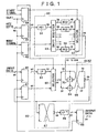
- Figs. 1 and 2 show an embodiment representing a calculating device of the present invention constructed as an encryption/decryption calculating device, wherein Fig. 2 shows details of a conversion circuit 70 in a calculator 60 included in Fig. 1.
- An encryption algorithm adopted in the encryption/decryption calculating device of this embodiment conforms with the encryption algorithm of DES.
- Key data secret key
- input data plain text data or encrypted text data
- a mode signal indicative of encryption or decryption is latched in a latch circuit 42 according to the clock CLK1. Further, the clock CLK1 is counted by a 16-stage counter 44 from the time point of a start signal.
- the key data outputted from the latch circuit 41, the mode signal outputted from the latch circuit 42 and the output signal from the counter 44 are supplied to a key generator 50, and key data K1 to K16 of sixteen stages each composed of 48 bits are outputted sequentially from the key generator 50.
- the 64-bit key data outputted from the latch circuit 41 are converted into 56-bit key data in a conversion circuit 51, and the 56-bit key data are shifted sequentially in a shift register 53, by one bit or two bits at a time, in accordance with the output signal of the latch circuit 42, whereby sixteen key data each composed of 56 bits are obtained.
- the sixteen 56-bit key data are each converted into 48-bit key data in a conversion circuit 55, and the sixteen 48-bit key data are sequentially selected, per pulse of the clock CLK1, in accordance with the output signal of the counter 44 in a selector 57, so that the aforementioned key data K1 to K16 are obtained sequentially per pulse of the clock CLK1.
- the key generator 50 there is performed a mere operation of generating 16-stage key data at a time from the input key data and selecting the data by the selector 57, wherein the key data K1 to K16 outputted from the key generator 50 are such that much noises (changes in the signal line potential) are superposed thereon in the vicinities of the change points.
- the output data (plain text data or encrypted text data) from the latch circuit 46 are supplied to a calculator 60.
- This calculator 60 is so formed that the calculations of sixteen stages are repeated cyclically by a one-stage calculating circuit in a calculator 100 shown in Fig. 5.
- the 64-bit data outputted from the latch circuit 46 are transposed bit by bit in an initial transposition circuit 61, and the 64-bit data after the initial transposition are outputted from a selector 62 controlled by the counter 44. Then the lower-order 32 bits out of the entire 64-bit data and the key data K1 are calculated together in a conversion circuit 70, where the data are converted by the use of a function F.
- the lower-order 32-bit data are transposed bit by bit in an expanded transposition circuit 71, and the same bit is selected plural times so that the above data are converted into 48-bit data, and thereafter the 48-bit data thus obtained and the 48-bit key data K1 are calculated together in an XOR circuit 73.
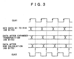
- Such operation of latching the output data of the XOR circuit 73 by the clock CLK2 different in phase from the clock CLK1 is performed for the reason that, since the output key data K1 to K16 of the key generator 50 and the output data of the expanded transposition circuit 71 are delayed from the change point (leading edge) of the clock CLK1 as shown in Fig. 3, the output data of the XOR circuit 73 are also delayed, and therefore, in case the output data of the XOR circuit 73 are latched according to the clock CLK1, the latched data are those preceding by one clock pulse. More concretely, for example, the clock CLK2 is set to be opposite in phase to the clock CLK1.
- the 48-bit data outputted from the latch circuit 75 are divided into eight data each composed of six bits, and each of the 6-bit data is replaced with 4-bit data according to a look-up table 77.
- the processing mentioned above is executed completely in the conversion circuit 70 during the first-stage calculation. Subsequently, the 32-bit data outputted from the transposition circuit 79 and the higher-order 32-bit data in the entire 64-bit data outputted from the selector 62 after the initial transposition are calculated in the XOR circuit 64 as the first-stage calculation.
- the calculation in the first stage is thus completed. Thereafter the 32-bit data inputted to the expanded transposition circuit 71 and the 32-bit data outputted from the XOR circuit 64 are combined together to form 64-bit data in such a manner that the higher-order 32 bits and the lower-order 32 bits are replaced mutually in a replacement/combination circuit 66, and the 64-bit data obtained after such combination are latched in the latch circuit 47 according to the clock CLK1.
- the output 64-bit data of the latch circuit 47 are outputted from the selector 62 instead of the output data from the initial transposition circuit 61, and the key data K2 or subsequent key data are inputted, instead of the key data K1, to the XOR circuit 73 in the conversion circuit 70, and the same calculation as the first-stage calculation is executed.
- replacing the higher-order 32 bits and the lower-order 32 bits in the replacement/combination circuit 66 is no longer necessary, and therefore the 64-bit data obtained after the replacement and combination in the circuit 66 are. supplied to a replacement circuit 67, where the higher-order 32 bits and the lower-order 32 bits are replaced with each other, and then the data are transposed bit by bit in an inverse transposition circuit 69.
- the 64-bit data after such inverse transposition are latched in the latch circuit 48 according to the clock CLK1, and then encrypted or decrypted data are outputted from the latch circuit 48.
- the power consumption is remarkably decreased as mentioned.
- the calculator 60 is so structured that calculations of 16 stages are executed through cyclic repetition by the one-stage calculating circuit, the number of gates in the calculating apparatus can be decreased to consequently reduce the circuit scale.
- the embodiment described above represents an exemplary case of complying with the DES encryption algorithm. However, it is not exactly necessary to comply with the DES encryption algorithm alone, and some modifications may be made by changing the bit lengths of the input data (plain text data or encrypted text data) and the key data, or increasing the number of stages of calculations.
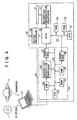
- Fig. 4 shows a data receiving system including a recording/reproducing apparatus as an embodiment of a data receiver of the present invention which is equipped with the encryption/decryption calculating device of the invention.
- encoded data encrypted by a secret key are received in a terminal unit 10 such as a PC through ripping from a recording medium 1 or down-loading from a delivery system 2 using the Internet.
- the encrypted data thus received are transmitted from the terminal unit 10 to a recording/reproducing apparatus 20 connected to a USB (Universal Serial Bus) terminal of the terminal unit 10.
- USB Universal Serial Bus
- the recording/reproducing apparatus 20 records the data on a recording medium 5 and reproduces the data therefrom.
- the apparatus 20 is equipped with an encryptor/decryptor 30.
- the encryptor/decryptor 30 comprises an encryption/decryption processor 40 consisting of the aforementioned encryption/decryption calculating device shown in Figs. 1 and 2, and also comprises a CPU 31 with a bus 32 which connects thereto a ROM 33 where programs and required fixed data are written for transfer of commands to be executed by the CPU 31 and also for encryption and decryption of the data, a RAM 34 functioning as a work area of the CPU 31, a USB interface 36 for transferring the command from and/or to the terminal unit 10 and acquiring the data from the terminal unit 10, an interface 37 for outputting the data to a DSP (Digital Signal Processor) 26 of the recording/reproducing apparatus, and an interface 39 for transferring the command from and/or to the CPU 21 of the recording/reproducing apparatus.
- a DSP Digital Signal Processor
- the encryptor/decryptor 30 is formed into a one-chip LSI (Large Scale Integration).
- a recording/reproducing apparatus there are connected, to a bus 22 of a CPU 21, a ROM 23 where programs to be executed by the CPU 21 and required fixed data are written, a RAM 24 functioning as a work area of the CPU 21, and the aforementioned DSP 26. And further a recording/reproduction processor 27 and an output processor 28 are connected to the DSP 26.
- the encoded data encrypted by the secret key and inputted from the terminal unit 10 via the USB interface 36 are decrypted as mentioned in the encryption/decryption processor 40, and the encoded data as decrypted plain text data are sent to the DSP 26 via the interface 37, and after being processed in the DSP 26, the data are recorded on the recording medium 5 by the recording/reproduction processor 27 or are delivered to the output terminal 29 after conversion into analog signal by the output processor 28.
- the recording medium 5 may be any of optical disk, hard disk, flexible disk, magnetic tape, memory card and semiconductor memory.
- the present invention is applicable not only to such recording/reproducing apparatus but also to an apparatus having no recording function and capable of merely receiving, decrypting and reproducing the encrypted data.
Landscapes
- Engineering & Computer Science (AREA)
- Computer Security & Cryptography (AREA)
- Computer Networks & Wireless Communication (AREA)
- Signal Processing (AREA)
- Physics & Mathematics (AREA)
- General Physics & Mathematics (AREA)
- Theoretical Computer Science (AREA)
- Storage Device Security (AREA)
Abstract
Description
- The present invention relates to a data calculating device and a data encryptor/decryptor for calculation of data to encrypt and/or decrypt the data.
- A device shown in Fig. 5 is contrived as an encryptor/decryptor conforming with an encryption algorithm of DES (Data Encryption Standard).
- Key data (secret key) and input data (plain text data or encrypted text data) are each composed of 64 bits and are latched in
latch circuits latch circuit 83 according to the clock CLK. - The key data outputted from the
latch circuit 81 are supplied to akey generator 90, and the key data K1 to K16 of 16 stages each composed of 48 bits are outputted sequentially from thekey generator 90. - More specifically, the 64-bit key data outputted from the
latch circuit 81 are converted into 56-bit key data in aconversion circuit 91, and higher-order 28-bit data and lower-order 28-bit data are shifted by 1 bit or 2 bits inshift circuits conversion circuit 95, whereby first-stage key data are generated. - Thereafter similar bit shift and conversion are executed, so that key data of 16 stages are generated and then are inputted to a
selector 99. Subsequently theselector 99 is controlled by the mode signal outputted from thelatch circuit 83, and key data K1 to K16 of 16 stages each composed of 48 bits are outputted sequentially according to the pulses of the clock CLK. - The output data (plain text data or encrypted text data) from the
latch circuit 82 are supplied to acalculator 100, where the following calculation is executed. - First, the 64-bit data outputted from the
latch circuit 82 are transposed bit by bit in aninitial transposition circuit 101, and the lower-order 32 bits out of the entire 64-bit data obtained after such initial transposition and the key data K1 are calculated together in a first-stage conversion circuit 102, and further after conversion by the use of a function F, the 32-bit data outputted from theconversion circuit 102 and the higher-order 32 bits out of the entire 64-bit data after the initial transposition are calculated together in an XOR (exclusive OR)circuit 103. - Subsequently, the 32-bit data outputted from the
XOR circuit 103 and the key data K2 are calculated together in a second-stage conversion circuit 104, and after conversion by the use of a function F, the 32-bit data outputted from theconversion circuit 104 and the lower-order 32 bits out of the entire 64-bit data obtained after the initial transposition are calculated together in anXOR circuit 105. - Thereafter, similarly to the above, the higher-
order 32 bits and the lower-order 32 bits are mutually replaced and, after execution of the calculations in the third and subsequent stages, the 32-bit data inputted to a 16th-stage conversion circuit 107 and the 32-bit data outputted from a 16th-stage XOR circuit 108 are combined with each other, and the 64-bit data obtained after such combination are transposed bit by bit in aninverse transposition circuit 109. - The 64-bit data after such inverse transposition are latched in a
latch circuit 84 according to the clock CLK, and then either encrypted or decrypted data are outputted from thelatch circuit 84. - However, in the encryption/decryption calculating device described above, the
key generator 90 is an asynchronous circuit including none of latch circuit (sampling circuit), wherein 16-stage key data are generated at a time from the input key data and are merely selected by theselector 99, so that much noises (changes in the signal line potential) are superposed, in the vicinities of the change points, on the key data K1 to K16 outputted from thekey generator 90, and therefore the power consumption in thecalculator 100 is increased. - In view of such problems, an object of the present invention resides in realizing an improved calculating device which is adapted for remarkable decrease of the power consumption.
- The calculating device of the present invention comprises first latch means for latching input data; first calculation means for calculating asynchronous data inputted from an asynchronous calculation circuit which performs an asynchronous operation, and also the input data latched in the first latch means; synchronizing means for synchronizing the calculated data outputted from the first calculation means; and a second calculation for further calculating the synchronized data obtained from the synchronizing means. In the calculating device of the above structure, the power consumption can be remarkably decreased and the circuit scale thereof is reducible.
-
- Fig. 1 is a block diagram showing an encryption/decryption calculating device as an embodiment which represents a calculating device of the present invention;
- Fig. 2 is a block diagram showing principal components in the encryption/decryption calculating device of Fig. 1;
- Fig. 3 is a diagram for explaining the operation performed in the encryption/decryption calculating device of Fig. 1;
- Fig. 4 is a block diagram showing a data recording/reproducing apparatus as an embodiment of a data receiver of the present invention; and
- Fig. 5 is a block diagram showing a conventional encryption/decryption calculating device.
- Figs. 1 and 2 show an embodiment representing a calculating device of the present invention constructed as an encryption/decryption calculating device, wherein Fig. 2 shows details of a
conversion circuit 70 in acalculator 60 included in Fig. 1. - An encryption algorithm adopted in the encryption/decryption calculating device of this embodiment conforms with the encryption algorithm of DES.
- Key data (secret key) and input data (plain text data or encrypted text data) are each composed of 64 bits and are latched in
latch circuits - And a mode signal indicative of encryption or decryption is latched in a
latch circuit 42 according to the clock CLK1. Further, the clock CLK1 is counted by a 16-stage counter 44 from the time point of a start signal. - The key data outputted from the
latch circuit 41, the mode signal outputted from thelatch circuit 42 and the output signal from thecounter 44 are supplied to akey generator 50, and key data K1 to K16 of sixteen stages each composed of 48 bits are outputted sequentially from thekey generator 50. - More specifically, the 64-bit key data outputted from the
latch circuit 41 are converted into 56-bit key data in aconversion circuit 51, and the 56-bit key data are shifted sequentially in ashift register 53, by one bit or two bits at a time, in accordance with the output signal of thelatch circuit 42, whereby sixteen key data each composed of 56 bits are obtained. - Further, the sixteen 56-bit key data are each converted into 48-bit key data in a
conversion circuit 55, and the sixteen 48-bit key data are sequentially selected, per pulse of the clock CLK1, in accordance with the output signal of thecounter 44 in aselector 57, so that the aforementioned key data K1 to K16 are obtained sequentially per pulse of the clock CLK1. - Thus, in the
key generator 50, there is performed a mere operation of generating 16-stage key data at a time from the input key data and selecting the data by theselector 57, wherein the key data K1 to K16 outputted from thekey generator 50 are such that much noises (changes in the signal line potential) are superposed thereon in the vicinities of the change points. - The output data (plain text data or encrypted text data) from the
latch circuit 46 are supplied to acalculator 60. Thiscalculator 60 is so formed that the calculations of sixteen stages are repeated cyclically by a one-stage calculating circuit in acalculator 100 shown in Fig. 5. - That is, first the 64-bit data outputted from the
latch circuit 46 are transposed bit by bit in aninitial transposition circuit 61, and the 64-bit data after the initial transposition are outputted from aselector 62 controlled by thecounter 44. Then the lower-order 32 bits out of the entire 64-bit data and the key data K1 are calculated together in aconversion circuit 70, where the data are converted by the use of a function F. - More specifically, in the
conversion circuit 70, as shown in Fig. 2, the lower-order 32-bit data are transposed bit by bit in an expandedtransposition circuit 71, and the same bit is selected plural times so that the above data are converted into 48-bit data, and thereafter the 48-bit data thus obtained and the 48-bit key data K1 are calculated together in anXOR circuit 73. - Further the 48-bit data outputted from the
XOR circuit 73 are latched in alatch circuit 75 according to a clock CLK2 different in phase from the foregoing clock CLK1. - Such operation of latching the output data of the
XOR circuit 73 by the clock CLK2 different in phase from the clock CLK1 is performed for the reason that, since the output key data K1 to K16 of thekey generator 50 and the output data of the expandedtransposition circuit 71 are delayed from the change point (leading edge) of the clock CLK1 as shown in Fig. 3, the output data of theXOR circuit 73 are also delayed, and therefore, in case the output data of theXOR circuit 73 are latched according to the clock CLK1, the latched data are those preceding by one clock pulse. More concretely, for example, the clock CLK2 is set to be opposite in phase to the clock CLK1. - As the output data of the
XOR circuit 73 are thus latched in thelatch circuit 75, the aforementioned noises in the output key data K1 to K16 of thekey generator 50 are absorbed, so that the potential of the output signal from thelatch circuit 75 is varied merely at the change point of the clock CLK2, hence achieving a remarkable reduction of the power consumption in the circuits posterior to thelatch circuit 75. - The 48-bit data outputted from the
latch circuit 75 are divided into eight data each composed of six bits, and each of the 6-bit data is replaced with 4-bit data according to a look-up table 77. - Further, the eight 4-bit data after such replacement are combined together to form 32-bit data, which are then transposed bit by bit in a
transposition circuit 79. - The processing mentioned above is executed completely in the
conversion circuit 70 during the first-stage calculation. Subsequently, the 32-bit data outputted from thetransposition circuit 79 and the higher-order 32-bit data in the entire 64-bit data outputted from theselector 62 after the initial transposition are calculated in theXOR circuit 64 as the first-stage calculation. - The calculation in the first stage is thus completed. Thereafter the 32-bit data inputted to the expanded
transposition circuit 71 and the 32-bit data outputted from theXOR circuit 64 are combined together to form 64-bit data in such a manner that the higher-order 32 bits and the lower-order 32 bits are replaced mutually in a replacement/combination circuit 66, and the 64-bit data obtained after such combination are latched in thelatch circuit 47 according to the clock CLK1. - In the calculation executed in each of the second and subsequent stages, the output 64-bit data of the
latch circuit 47 are outputted from theselector 62 instead of the output data from theinitial transposition circuit 61, and the key data K2 or subsequent key data are inputted, instead of the key data K1, to theXOR circuit 73 in theconversion circuit 70, and the same calculation as the first-stage calculation is executed. - After completion of the calculation in the 16th stage, replacing the higher-
order 32 bits and the lower-order 32 bits in the replacement/combination circuit 66 is no longer necessary, and therefore the 64-bit data obtained after the replacement and combination in thecircuit 66 are. supplied to areplacement circuit 67, where the higher-order 32 bits and the lower-order 32 bits are replaced with each other, and then the data are transposed bit by bit in aninverse transposition circuit 69. - The 64-bit data after such inverse transposition are latched in the
latch circuit 48 according to the clock CLK1, and then encrypted or decrypted data are outputted from thelatch circuit 48. - In the encryption/decryption calculating device of this embodiment, the power consumption is remarkably decreased as mentioned. Moreover, since the
calculator 60 is so structured that calculations of 16 stages are executed through cyclic repetition by the one-stage calculating circuit, the number of gates in the calculating apparatus can be decreased to consequently reduce the circuit scale. - The embodiment described above represents an exemplary case of complying with the DES encryption algorithm. However, it is not exactly necessary to comply with the DES encryption algorithm alone, and some modifications may be made by changing the bit lengths of the input data (plain text data or encrypted text data) and the key data, or increasing the number of stages of calculations.
- Fig. 4 shows a data receiving system including a recording/reproducing apparatus as an embodiment of a data receiver of the present invention which is equipped with the encryption/decryption calculating device of the invention.
- In the data receiving system of this example, encoded data encrypted by a secret key are received in a
terminal unit 10 such as a PC through ripping from arecording medium 1 or down-loading from adelivery system 2 using the Internet. - The encrypted data thus received are transmitted from the
terminal unit 10 to a recording/reproducingapparatus 20 connected to a USB (Universal Serial Bus) terminal of theterminal unit 10. - The recording/reproducing
apparatus 20 records the data on arecording medium 5 and reproduces the data therefrom. Theapparatus 20 is equipped with an encryptor/decryptor 30. - The encryptor/
decryptor 30 comprises an encryption/decryption processor 40 consisting of the aforementioned encryption/decryption calculating device shown in Figs. 1 and 2, and also comprises aCPU 31 with abus 32 which connects thereto aROM 33 where programs and required fixed data are written for transfer of commands to be executed by theCPU 31 and also for encryption and decryption of the data, aRAM 34 functioning as a work area of theCPU 31, aUSB interface 36 for transferring the command from and/or to theterminal unit 10 and acquiring the data from theterminal unit 10, aninterface 37 for outputting the data to a DSP (Digital Signal Processor) 26 of the recording/reproducing apparatus, and aninterface 39 for transferring the command from and/or to theCPU 21 of the recording/reproducing apparatus. - The encryptor/
decryptor 30 is formed into a one-chip LSI (Large Scale Integration). - In the recording/reproducing apparatus, there are connected, to a
bus 22 of aCPU 21, aROM 23 where programs to be executed by theCPU 21 and required fixed data are written, aRAM 24 functioning as a work area of theCPU 21, and theaforementioned DSP 26. And further a recording/reproduction processor 27 and anoutput processor 28 are connected to theDSP 26. - In the encryptor/
decryptor 30, the encoded data encrypted by the secret key and inputted from theterminal unit 10 via theUSB interface 36 are decrypted as mentioned in the encryption/decryption processor 40, and the encoded data as decrypted plain text data are sent to theDSP 26 via theinterface 37, and after being processed in theDSP 26, the data are recorded on therecording medium 5 by the recording/reproduction processor 27 or are delivered to theoutput terminal 29 after conversion into analog signal by theoutput processor 28. - The
recording medium 5 may be any of optical disk, hard disk, flexible disk, magnetic tape, memory card and semiconductor memory. - The present invention is applicable not only to such recording/reproducing apparatus but also to an apparatus having no recording function and capable of merely receiving, decrypting and reproducing the encrypted data.
- According to the present invention, as described hereinabove, it becomes possible to realize an improved calculating device where the power consumption is remarkably decreased.
Claims (9)
- A calculating device comprising:first latch means for latching input data;first calculation means for calculating the output data of said first latch means and data obtained from an asynchronous circuit;second latch means for latching the output data of said first calculation means; andsecond calculation means for calculating the output data of said second latch means.
- A calculating device comprising:first latch means for latching input data;first calculation means for calculating asynchronous data inputted from an asynchronous calculation circuit which performs an asynchronous operation, and the input data latched in said first latch means;synchronizing means for synchronizing the data calculated in and outputted from said first calculation means; andsecond calculation means for further calculating the data synchronized in said synchronizing means.
- The calculating device according to claim 2, wherein the latch timing of said first latch means and the synchronization timing of said synchronizing means are different from each other.
- The calculating device according to claim 2, further comprising:second latch means for latching the second calculated data outputted from said second calculation means; andselection means for selecting the input data latched in said second latch means or the data synchronized by said synchronizing means;wherein said first calculation means executes a predetermined calculation of the data selected by said selection means, i.e., either the input data latched in said first latch means or the data synchronized by said synchronizing means, and the asynchronous data inputted from said asynchronous calculation circuit.
- The calculating device according to claim 2, further comprising:selective signal generating means for enabling said selection means to select, at a predetermined timing, either the input data latched in said second latch means or the data synchronized by said synchronizing means;wherein the input data latched in said first latch means are calculated under control a plurality of times by said first and second calculation means.
- An encryptor/decryptor comprising:asynchronous calculation processing means for executing an asynchronous calculation of input key data in accordance with input processing mode data;first calculation means for executing a first calculation of input data in accordance with the calculated key data obtained from said asynchronous calculation processing means;synchronizing means for synchronizing the first calculation result data outputted from said first calculation means;second calculation means for further executing a second calculation of the synchronized data outputted from said synchronizing means;selection means for selecting either the input calculation data to be processed or the second calculation result data outputted from said second calculation means and input to said first calculation means; andselection timing control means for controlling the selection timing of said selection means;wherein the input calculation data are processed, under control of said selection timing control means, through the first calculation and the second calculation a plurality of times in accordance with the input calculation key data.
- The encryptor/decryptor according to claim 6, wherein said asynchronous calculation processing means generates a plurality of key data from the input key data in accordance with said processing mode.
- The encryptor/decryptor according to claim 6, further comprising:first transposition means for transposing the bits of the input calculation data;second transposition means for transposing the bits of the selected data outputted from said selection means;third transposition means for transposing the bits of the second calculation result data outputted from said second calculation means;fourth calculation means for further executing a predetermined calculation of the transposed data obtained from said third transposition means; andfourth transposition means for transposing the bits of the fourth calculation result data outputted from said fourth calculation means.
- The encryptor/decryptor according to claim 6, wherein the selection timing of said selection means and the synchronization timing of said synchronizing means are different from each other.
Applications Claiming Priority (3)
| Application Number | Priority Date | Filing Date | Title |
|---|---|---|---|
| JP2002118508 | 2002-04-19 | ||
| JP2002118508A JP4150886B2 (en) | 2002-04-19 | 2002-04-19 | Encryption / decryption operation device and data receiving device |
| PCT/JP2003/005011 WO2003090187A1 (en) | 2002-04-19 | 2003-04-18 | Arithmetic device and encryption/decryption device |
Publications (3)
| Publication Number | Publication Date |
|---|---|
| EP1403840A1 true EP1403840A1 (en) | 2004-03-31 |
| EP1403840A4 EP1403840A4 (en) | 2010-08-04 |
| EP1403840B1 EP1403840B1 (en) | 2013-06-05 |
Family
ID=29243529
Family Applications (1)
| Application Number | Title | Priority Date | Filing Date |
|---|---|---|---|
| EP03720936.8A Expired - Lifetime EP1403840B1 (en) | 2002-04-19 | 2003-04-18 | Arithmetic device and encryption/decryption device |
Country Status (6)
| Country | Link |
|---|---|
| US (1) | US7564972B2 (en) |
| EP (1) | EP1403840B1 (en) |
| JP (1) | JP4150886B2 (en) |
| KR (1) | KR100986226B1 (en) |
| CN (1) | CN1273946C (en) |
| WO (1) | WO2003090187A1 (en) |
Families Citing this family (4)
| Publication number | Priority date | Publication date | Assignee | Title |
|---|---|---|---|---|
| US20060053495A1 (en) * | 2002-10-21 | 2006-03-09 | Omron Corporation | Medium data reproduction device, medium data distribution device, medium data reproduction method, medium data reproduction program, medium data distrubution program, and computer-readable recording |
| CN1777089B (en) * | 2005-11-24 | 2010-11-17 | 上海森田科学技术研究所有限公司 | Complex phase shift encrypting and decrypting method |
| US20080095228A1 (en) * | 2006-10-20 | 2008-04-24 | Nokia Corporation | System and method for providing picture output indications in video coding |
| CN101397545B (en) * | 2008-09-23 | 2010-09-01 | 浙江林学院 | O-nitrobenzaldehyde degrading bacteria and use thereof |
Family Cites Families (13)
| Publication number | Priority date | Publication date | Assignee | Title |
|---|---|---|---|---|
| US4100374A (en) * | 1977-04-11 | 1978-07-11 | Bell Telephone Laboratories, Incorporated | Uniform permutation privacy system |
| US4789959A (en) * | 1985-03-05 | 1988-12-06 | Intersil, Inc. | Delay circuit for a real time clock |
| KR910002236B1 (en) * | 1986-08-04 | 1991-04-08 | 미쓰비시 뎅기 가부시끼가이샤 | Semiconductor integrated circuit device |
| JPH1022990A (en) | 1996-06-28 | 1998-01-23 | Sony Corp | Information processing apparatus and method |
| KR100223026B1 (en) * | 1996-10-17 | 1999-10-01 | 정선종 | Synchronizing circuit |
| JP3088337B2 (en) | 1997-05-30 | 2000-09-18 | 三菱電機株式会社 | Cryptographic processing device, IC card and cryptographic processing method |
| JP3119624B2 (en) | 1998-06-16 | 2000-12-25 | 日本電気株式会社 | Noise removing device, noise removing method, and recording medium |
| DE60024941T8 (en) * | 1999-08-31 | 2006-08-10 | Matsushita Electric Industrial Co., Ltd., Kadoma | Encryption method and apparatus, decryption method and apparatus |
| KR100377175B1 (en) * | 2000-06-08 | 2003-03-26 | 주식회사 하이닉스반도체 | Encryption device using data encryption standard algorithm |
| KR100377176B1 (en) | 2000-06-12 | 2003-03-26 | 주식회사 하이닉스반도체 | Encryption device using data encryption standard algorithm |
| US7155011B2 (en) * | 2001-03-13 | 2006-12-26 | Victor Company Of Japan, Limited | Encryption method, decryption method, and recording and reproducing apparatus |
| JP2002328845A (en) * | 2001-05-07 | 2002-11-15 | Fujitsu Ltd | Semiconductor integrated circuit and IC card security protection method |
| JP3851115B2 (en) * | 2001-06-28 | 2006-11-29 | 富士通株式会社 | Cryptographic circuit |
-
2002
- 2002-04-19 JP JP2002118508A patent/JP4150886B2/en not_active Expired - Fee Related
-
2003
- 2003-04-18 CN CNB038004798A patent/CN1273946C/en not_active Expired - Fee Related
- 2003-04-18 EP EP03720936.8A patent/EP1403840B1/en not_active Expired - Lifetime
- 2003-04-18 KR KR1020037016561A patent/KR100986226B1/en not_active Expired - Fee Related
- 2003-04-18 US US10/481,239 patent/US7564972B2/en not_active Expired - Fee Related
- 2003-04-18 WO PCT/JP2003/005011 patent/WO2003090187A1/en not_active Ceased
Also Published As
| Publication number | Publication date |
|---|---|
| JP4150886B2 (en) | 2008-09-17 |
| US7564972B2 (en) | 2009-07-21 |
| JP2003316260A (en) | 2003-11-07 |
| WO2003090187A1 (en) | 2003-10-30 |
| KR20040100853A (en) | 2004-12-02 |
| EP1403840A4 (en) | 2010-08-04 |
| EP1403840B1 (en) | 2013-06-05 |
| US20040196976A1 (en) | 2004-10-07 |
| CN1273946C (en) | 2006-09-06 |
| KR100986226B1 (en) | 2010-10-07 |
| CN1518733A (en) | 2004-08-04 |
Similar Documents
| Publication | Publication Date | Title |
|---|---|---|
| JP4127472B2 (en) | Data conversion apparatus, data conversion method and program for data conversion apparatus, and computer-readable recording medium | |
| US8750498B1 (en) | Method and apparatus for encoding data in accordance with the advanced encryption standard (AES) | |
| JP4491706B2 (en) | Encryption / decryption device and data reception device | |
| WO2003100751A1 (en) | Data conversion device and data conversion method | |
| JPH11136229A (en) | Method and system for generating encryption key | |
| JPWO2009087972A1 (en) | Data transmitting apparatus, data receiving apparatus, methods thereof, computer program, and data communication system thereof | |
| JP5605197B2 (en) | Cryptographic processing apparatus, cryptographic processing method, and program | |
| JP4740611B2 (en) | A key scheduler that selectively generates an encryption round key and a decryption round key corresponding to an initial round key having a variable key length | |
| US7564972B2 (en) | Arithmetic device and encryption/decryption device | |
| CN1795637B (en) | Method and apparatus for a low memory hardware implementation of the key expansion function | |
| CN100524150C (en) | Block cipher method and block encryption/decryption circuit | |
| JPH09251267A (en) | Encryption device and encryption method | |
| KR100668664B1 (en) | Encryption / decryption apparatus and method using AES linedal block algorithm | |
| KR102348802B1 (en) | AES encryption and decryption circuit | |
| JP2006502437A (en) | Encryption circuit apparatus and method | |
| JPH06276187A (en) | Cryptographic device | |
| Varma | Fast Pipelined Aes Algorithm Implemented on Xilinx Fpgas | |
| JPH0385835A (en) | Cryptographic system employing cyclic code logic | |
| JP2006292958A (en) | Encryption device and decryption device | |
| JPH09298534A (en) | Decoding circuit |
Legal Events
| Date | Code | Title | Description |
|---|---|---|---|
| PUAI | Public reference made under article 153(3) epc to a published international application that has entered the european phase |
Free format text: ORIGINAL CODE: 0009012 |
|
| 17P | Request for examination filed |
Effective date: 20031219 |
|
| AK | Designated contracting states |
Kind code of ref document: A1 Designated state(s): AT BE BG CH CY CZ DE DK EE ES FI FR GB GR HU IE IT LI LU MC NL PT RO SE SI SK TR |
|
| A4 | Supplementary search report drawn up and despatched |
Effective date: 20100701 |
|
| 17Q | First examination report despatched |
Effective date: 20101103 |
|
| REG | Reference to a national code |
Ref country code: DE Ref legal event code: R079 Ref document number: 60344215 Country of ref document: DE Free format text: PREVIOUS MAIN CLASS: G09C0001000000 Ipc: H04L0009060000 |
|
| RIC1 | Information provided on ipc code assigned before grant |
Ipc: H04L 9/00 20060101ALI20121031BHEP Ipc: H04L 9/06 20060101AFI20121031BHEP |
|
| GRAP | Despatch of communication of intention to grant a patent |
Free format text: ORIGINAL CODE: EPIDOSNIGR1 |
|
| RBV | Designated contracting states (corrected) |
Designated state(s): DE FR GB |
|
| GRAS | Grant fee paid |
Free format text: ORIGINAL CODE: EPIDOSNIGR3 |
|
| GRAA | (expected) grant |
Free format text: ORIGINAL CODE: 0009210 |
|
| AK | Designated contracting states |
Kind code of ref document: B1 Designated state(s): DE FR GB |
|
| REG | Reference to a national code |
Ref country code: GB Ref legal event code: FG4D |
|
| REG | Reference to a national code |
Ref country code: DE Ref legal event code: R096 Ref document number: 60344215 Country of ref document: DE Effective date: 20130801 |
|
| PLBE | No opposition filed within time limit |
Free format text: ORIGINAL CODE: 0009261 |
|
| STAA | Information on the status of an ep patent application or granted ep patent |
Free format text: STATUS: NO OPPOSITION FILED WITHIN TIME LIMIT |
|
| 26N | No opposition filed |
Effective date: 20140306 |
|
| REG | Reference to a national code |
Ref country code: DE Ref legal event code: R097 Ref document number: 60344215 Country of ref document: DE Effective date: 20140306 |
|
| PGFP | Annual fee paid to national office [announced via postgrant information from national office to epo] |
Ref country code: DE Payment date: 20140418 Year of fee payment: 12 |
|
| GBPC | Gb: european patent ceased through non-payment of renewal fee |
Effective date: 20140418 |
|
| REG | Reference to a national code |
Ref country code: FR Ref legal event code: ST Effective date: 20141231 |
|
| PG25 | Lapsed in a contracting state [announced via postgrant information from national office to epo] |
Ref country code: GB Free format text: LAPSE BECAUSE OF NON-PAYMENT OF DUE FEES Effective date: 20140418 |
|
| PG25 | Lapsed in a contracting state [announced via postgrant information from national office to epo] |
Ref country code: FR Free format text: LAPSE BECAUSE OF NON-PAYMENT OF DUE FEES Effective date: 20140430 |
|
| REG | Reference to a national code |
Ref country code: DE Ref legal event code: R119 Ref document number: 60344215 Country of ref document: DE |
|
| PG25 | Lapsed in a contracting state [announced via postgrant information from national office to epo] |
Ref country code: DE Free format text: LAPSE BECAUSE OF NON-PAYMENT OF DUE FEES Effective date: 20151103 |