EP1403816A2 - Method of mounting a hybrid IC card and hybrid IC card - Google Patents
Method of mounting a hybrid IC card and hybrid IC card Download PDFInfo
- Publication number
- EP1403816A2 EP1403816A2 EP03020949A EP03020949A EP1403816A2 EP 1403816 A2 EP1403816 A2 EP 1403816A2 EP 03020949 A EP03020949 A EP 03020949A EP 03020949 A EP03020949 A EP 03020949A EP 1403816 A2 EP1403816 A2 EP 1403816A2
- Authority
- EP
- European Patent Office
- Prior art keywords
- card
- antenna
- module
- circuit
- lsi
- Prior art date
- Legal status (The legal status is an assumption and is not a legal conclusion. Google has not performed a legal analysis and makes no representation as to the accuracy of the status listed.)
- Granted
Links
Images


Classifications
-
- G—PHYSICS
- G06—COMPUTING OR CALCULATING; COUNTING
- G06K—GRAPHICAL DATA READING; PRESENTATION OF DATA; RECORD CARRIERS; HANDLING RECORD CARRIERS
- G06K19/00—Record carriers for use with machines and with at least a part designed to carry digital markings
- G06K19/06—Record carriers for use with machines and with at least a part designed to carry digital markings characterised by the kind of the digital marking, e.g. shape, nature, code
- G06K19/067—Record carriers with conductive marks, printed circuits or semiconductor circuit elements, e.g. credit or identity cards also with resonating or responding marks without active components
- G06K19/07—Record carriers with conductive marks, printed circuits or semiconductor circuit elements, e.g. credit or identity cards also with resonating or responding marks without active components with integrated circuit chips
-
- G—PHYSICS
- G06—COMPUTING OR CALCULATING; COUNTING
- G06K—GRAPHICAL DATA READING; PRESENTATION OF DATA; RECORD CARRIERS; HANDLING RECORD CARRIERS
- G06K19/00—Record carriers for use with machines and with at least a part designed to carry digital markings
- G06K19/06—Record carriers for use with machines and with at least a part designed to carry digital markings characterised by the kind of the digital marking, e.g. shape, nature, code
- G06K19/067—Record carriers with conductive marks, printed circuits or semiconductor circuit elements, e.g. credit or identity cards also with resonating or responding marks without active components
- G06K19/07—Record carriers with conductive marks, printed circuits or semiconductor circuit elements, e.g. credit or identity cards also with resonating or responding marks without active components with integrated circuit chips
- G06K19/077—Constructional details, e.g. mounting of circuits in the carrier
- G06K19/07749—Constructional details, e.g. mounting of circuits in the carrier the record carrier being capable of non-contact communication, e.g. constructional details of the antenna of a non-contact smart card
- G06K19/07766—Constructional details, e.g. mounting of circuits in the carrier the record carrier being capable of non-contact communication, e.g. constructional details of the antenna of a non-contact smart card comprising at least a second communication arrangement in addition to a first non-contact communication arrangement
- G06K19/07769—Constructional details, e.g. mounting of circuits in the carrier the record carrier being capable of non-contact communication, e.g. constructional details of the antenna of a non-contact smart card comprising at least a second communication arrangement in addition to a first non-contact communication arrangement the further communication means being a galvanic interface, e.g. hybrid or mixed smart cards having a contact and a non-contact interface
-
- G—PHYSICS
- G06—COMPUTING OR CALCULATING; COUNTING
- G06K—GRAPHICAL DATA READING; PRESENTATION OF DATA; RECORD CARRIERS; HANDLING RECORD CARRIERS
- G06K19/00—Record carriers for use with machines and with at least a part designed to carry digital markings
- G06K19/06—Record carriers for use with machines and with at least a part designed to carry digital markings characterised by the kind of the digital marking, e.g. shape, nature, code
- G06K19/067—Record carriers with conductive marks, printed circuits or semiconductor circuit elements, e.g. credit or identity cards also with resonating or responding marks without active components
- G06K19/07—Record carriers with conductive marks, printed circuits or semiconductor circuit elements, e.g. credit or identity cards also with resonating or responding marks without active components with integrated circuit chips
- G06K19/0723—Record carriers with conductive marks, printed circuits or semiconductor circuit elements, e.g. credit or identity cards also with resonating or responding marks without active components with integrated circuit chips the record carrier comprising an arrangement for non-contact communication, e.g. wireless communication circuits on transponder cards, non-contact smart cards or RFIDs
- G06K19/0726—Record carriers with conductive marks, printed circuits or semiconductor circuit elements, e.g. credit or identity cards also with resonating or responding marks without active components with integrated circuit chips the record carrier comprising an arrangement for non-contact communication, e.g. wireless communication circuits on transponder cards, non-contact smart cards or RFIDs the arrangement including a circuit for tuning the resonance frequency of an antenna on the record carrier
-
- G—PHYSICS
- G06—COMPUTING OR CALCULATING; COUNTING
- G06K—GRAPHICAL DATA READING; PRESENTATION OF DATA; RECORD CARRIERS; HANDLING RECORD CARRIERS
- G06K19/00—Record carriers for use with machines and with at least a part designed to carry digital markings
- G06K19/06—Record carriers for use with machines and with at least a part designed to carry digital markings characterised by the kind of the digital marking, e.g. shape, nature, code
- G06K19/067—Record carriers with conductive marks, printed circuits or semiconductor circuit elements, e.g. credit or identity cards also with resonating or responding marks without active components
- G06K19/07—Record carriers with conductive marks, printed circuits or semiconductor circuit elements, e.g. credit or identity cards also with resonating or responding marks without active components with integrated circuit chips
- G06K19/077—Constructional details, e.g. mounting of circuits in the carrier
-
- G—PHYSICS
- G06—COMPUTING OR CALCULATING; COUNTING
- G06K—GRAPHICAL DATA READING; PRESENTATION OF DATA; RECORD CARRIERS; HANDLING RECORD CARRIERS
- G06K19/00—Record carriers for use with machines and with at least a part designed to carry digital markings
- G06K19/06—Record carriers for use with machines and with at least a part designed to carry digital markings characterised by the kind of the digital marking, e.g. shape, nature, code
- G06K19/067—Record carriers with conductive marks, printed circuits or semiconductor circuit elements, e.g. credit or identity cards also with resonating or responding marks without active components
- G06K19/07—Record carriers with conductive marks, printed circuits or semiconductor circuit elements, e.g. credit or identity cards also with resonating or responding marks without active components with integrated circuit chips
- G06K19/077—Constructional details, e.g. mounting of circuits in the carrier
- G06K19/07745—Mounting details of integrated circuit chips
-
- G—PHYSICS
- G06—COMPUTING OR CALCULATING; COUNTING
- G06K—GRAPHICAL DATA READING; PRESENTATION OF DATA; RECORD CARRIERS; HANDLING RECORD CARRIERS
- G06K19/00—Record carriers for use with machines and with at least a part designed to carry digital markings
- G06K19/06—Record carriers for use with machines and with at least a part designed to carry digital markings characterised by the kind of the digital marking, e.g. shape, nature, code
- G06K19/067—Record carriers with conductive marks, printed circuits or semiconductor circuit elements, e.g. credit or identity cards also with resonating or responding marks without active components
- G06K19/07—Record carriers with conductive marks, printed circuits or semiconductor circuit elements, e.g. credit or identity cards also with resonating or responding marks without active components with integrated circuit chips
- G06K19/077—Constructional details, e.g. mounting of circuits in the carrier
- G06K19/07749—Constructional details, e.g. mounting of circuits in the carrier the record carrier being capable of non-contact communication, e.g. constructional details of the antenna of a non-contact smart card
-
- H—ELECTRICITY
- H10—SEMICONDUCTOR DEVICES; ELECTRIC SOLID-STATE DEVICES NOT OTHERWISE PROVIDED FOR
- H10W—GENERIC PACKAGES, INTERCONNECTIONS, CONNECTORS OR OTHER CONSTRUCTIONAL DETAILS OF DEVICES COVERED BY CLASS H10
- H10W90/00—Package configurations
- H10W90/701—Package configurations characterised by the relative positions of pads or connectors relative to package parts
- H10W90/751—Package configurations characterised by the relative positions of pads or connectors relative to package parts of bond wires
- H10W90/754—Package configurations characterised by the relative positions of pads or connectors relative to package parts of bond wires between a chip and a stacked insulating package substrate, interposer or RDL
Definitions
- the present invention relates to a method of mounting a combination-type IC card which can carry out data communication with an external terminal with both contact and contactless interfaces.
- the combination-type card is an IC card which can carry out the data communication with the external terminal with both the contact and contactless interfaces.
- the resonance circuit is formed with a pattern capacitor in which a conductor is sandwiched between both sides of a circuit substrate, and a patterned antenna, and LSI. Sometimes the capacitor is incorporated in LSI.
- the IC card is a combination-type IC card 1 which can carry out data communication with a card reader/writer as an external terminal with both contact and contactless (wireless) interfaces.
- the combination-type IC card 1 has a tuning circuit 8 which includes an antenna 3 and tuning capacitors for trimming (pattern capacitor) 4, 5, 6, and 7 in an antenna card 2 and an IC module 9 which is electrically connected to the tuning circuit and is mounted on the antenna card 2.
- a tuning circuit 8 which includes an antenna 3 and tuning capacitors for trimming (pattern capacitor) 4, 5, 6, and 7 in an antenna card 2 and an IC module 9 which is electrically connected to the tuning circuit and is mounted on the antenna card 2.
- the IC module 9 a substrate 10, an LSI 11 which is mounted on the substrate 10 by wire bonding, a contact portion 12 which is mounted on the other side of the LSI 11 of the substrate 10, and pads for connection 13 and 14.
- a resonance circuit includes the tuning circuit 8 and LSI 11.
- the contact portion 12 includes, e.g. a plurality of terminals 12a to 12h, which have a VCC terminal 12a for operational power voltage (+5V), an RST terminal 12b for a reset signal, a CLK terminal 12c for a clock signal, a GND terminal 12d for ground, a VPP terminal 12e for write power voltage of memory, an I/O terminal 12f for data input/output, and spare terminals 12g and 12h.
- FIG. 3 is an equivalent circuit of the combination-type IC card 1 according to the invention.
- the resonance circuit is formed by the antenna 3, the tuning capacitors 4, 5, 6, and 7, and the LSI 11.
- the combination-type IC card 1 carries out the contactless data communication in such a manner that the combination-type IC card 1 converts radio waves supplied from the outside of the card into electric power to operate the LSI 11 and transmits a response using the remaining electric power.
- the data communication is carried out through the contact portion 12.
- the resonance frequency of the combination-type IC card 1 is turned to a specific frequency.
- parts (Pa and Pd) of a pattern (signal line) that connects the capacitors 4 to 7 to the antenna 3 are cut, changing the capacitance of the resonant circuit and thus achieving trimming.
- the LSI 11 includes a power generating circuit 21, a demodulating circuit 22, a control logic circuit 23, a modulating circuit 24, a memory 25, a clock generating circuit 26, and an interface 27.
- the tuning circuit 8 receives a signal of the radio waves from the card reader/writer.
- the demodulating circuit 22 demodulates the received signal to transmit it to the control logic circuit 23, and the control logic circuit 23 carries out command analysis. Then, the control logic circuit 23 writes data in the memory 25 or reads data from the memory 25 according to the contents of the command.
- the control logic circuit 23 reads the data from the memory 25 to transmit it to the modulating circuit 24. The data is modulated with the modulating circuit 24 and transmitted to the card reader/writer by the radio waves using the tuning circuit 8.
- the powec generating circuit 21 generates the electric power consumed in the wireless card 1 from the received signal with the tuning circuit 8.
- the clock generating circuit 26 generates a clock required to operate each circuit from the received signal with the tuning circuit 8, and the clock is outputted to the demodulating circuit 22, the modulating circuit 24, and the control logic circuit 23.
- the combination-type IC card 1 carries out the contactless data communication in such a manner that the combination-type IC card 1 converts the radio waves supplied from the outside of the card (card reader/writer) into the electric power to operate the LSI 11 and transmits the response using the remaining electric power.
- the interface 27 is connected to the contact portion 12, and the interface 27 carries out exchange of the data between the control logic circuit 23 and the external device (card reader/writer), which is connected to the contact portion 12 or in contact with the contact portion 12.
- FIG. 5 shows an antenna substrate used in the invention.
- an antenna substrate 31 polyethylene terephthalate (hereinafter referred to as PET, not shown) having a thickness of 0.025 mm is used as a base material.
- Antenna terminals 32 and 33 and electrodes 4a, 5a, 6a, and 7a of the tuning capacitors 4, 5, 6, and 7, which connect the antenna 3 and the IC module 9, are formed by etching aluminum foil on one side of the antenna substrate 31.
- the other electrodes 4b, 5b, 6b, and 7b of the tuning capacitors 4, 5, 6, and 7, made of the same aluminum foil, are formed on the other side of the antenna substrate 31.
- the tuning capacitors 4, 5, 6, and 7 have electrostatic capacity by sandwiching dielectric PET between conductive electrodes.
- the tuning capacitors 4, 5, 6, and 7 become the capacitor having an electrode area of 1 cm ⁇ 1 cm and the capacitance of 80 pF.
- One end of the antenna 3 is wired to the electrodes 4a, 5a, 6a, and 7a of the tuning capacitors 4, 5, 6, and 7, and the other end of the antenna 3 is wired to the electrodes 4b, 5b, 6b, and 7b of the tuning capacitors 4, 5, 6, and 7.
- the tuning capacitors for trimming 4, 5, 6, and 7 are changed by simultaneously cutting their patterns in a milling step.
- a correction value is determined by previous measurement in which a probe touches on the pads 13 and 14 of the IC module 9.
- wire bonding is adopted in the mounting method of the LSI 11, other methods such as a flip-chip method may be adopted.
- FIGS. 6 to 8 show a process flow of the combination-type IC card 1 according to the invention.
- PET sheets or PVC sheets 34 and 35 are integrally formed on the both sides of the antenna substrate 31.
- the milling is carried out at a predetermined position of the antenna card 36 in order to make holes 41 and 42 implanting the IC module 9, and the IC module 9 is implanted in an implanting step to make the combination-type IC card 1.
- the resonance frequency has a value in which the capacitances of the antenna 3, the tuning capacitors 4, 5, 6, and 7, and the LSI 11 are added.
- the invention proposes a measure which selects and cuts the tuning capacitors 4, 5, 6, and 7 in order that the variation in the capacitance of the capacitor inside the LSI 11 is corrected to establish resonance at the predetermined frequency.
- FIGS. 1, 7, and 10 show an external view and a sectional view of the card in which the milling step has been completed.
- a shallow bonding hole 41 for bonding the IC module 9 and a deep bonding hole 42 for storing an LSI molding portion are present in the card, while the holes are in the concave form from the surface of the card.
- the parts (cut portions Pa to Pe) of the pattern connecting the antenna 3 and the capacitors 4, 5, 6, and 7 are exposed toward bottom sides of the bonding hole 41 for the IC module 9.
- the cut portions Pa and Pb of the capacitor pattern (signal line) connected to the tuning capacitors 4 and 5 are cut to adjust the capacitance in the trimming step.
- the cut portions Pa and Pb of the capacitor pattern are cut with a cutter used in the milling at the same time when the milling step is carried out, so that the dedicated cutter for trimming is not particularly required.
- the pattern may be cut with the cutter for trimming.
- this can prevent the risk that the conductive bonding agent overflows and the cut capacitor is connected again in the case that the antenna connecting terminals 32 and 33 and the cut portions Pa to Pd of the capacitor pattern are provided on the same side.
- the IC module 9 to which an anisotropic conductive bonding film (not shown) is pre-bonded is dropped into the bonding holes 41 and 42, pressed with heat, and electrically and physically connected to form the combination-type IC card 1 shown in FIG. 12.
- the tuning circuit 8 and the LSI 11 are connected in such a manner that the pads 13 and 14 of the IC module 9 are connected to the antenna connecting terminals 32 and 33, respectively.
- the capacitance of the capacitor inside the LSI 11 slightly has the variation from the manufacturing lot of the LSI 11, its influence causes the resonance frequency to be outside a target resonance frequency f.
- the tuning capacitors for trimming 4, 5, 6, and 7 are selected and connected. As a result, even in the case of the combination-type IC card, a certain communication range can be obtained.
- cut portions Ps to Pd of the capacitor pattern are arranged at the side different from the sides where the antenna connecting terminals 32 and 33 are located in the embodiment, the invention is not limited to the embodiment, and as shown in FIG. 13, the cut portions Ps to Pd of the capacitor pattern and the antenna connecting terminal 32 or 33 may be arranged at the same side.
Landscapes
- Engineering & Computer Science (AREA)
- Computer Hardware Design (AREA)
- Microelectronics & Electronic Packaging (AREA)
- Physics & Mathematics (AREA)
- General Physics & Mathematics (AREA)
- Theoretical Computer Science (AREA)
- Computer Networks & Wireless Communication (AREA)
- Credit Cards Or The Like (AREA)
- Parts Printed On Printed Circuit Boards (AREA)
Abstract
Description
- The present invention relates to a method of mounting a combination-type IC card which can carry out data communication with an external terminal with both contact and contactless interfaces.
- The combination-type card is an IC card which can carry out the data communication with the external terminal with both the contact and contactless interfaces.
- When the card is operated with the contactless interface, since it is necessary to receive electric power supply by tuning a resonance circuit in the card to a transmitted frequency from a wireless card reader/writer, the resonance circuit is formed with a pattern capacitor in which a conductor is sandwiched between both sides of a circuit substrate, and a patterned antenna, and LSI. Sometimes the capacitor is incorporated in LSI.
- In the prior art, since a step in which the resonance circuit is tuned to a specific frequency (trimming step) is absent in a process of manufacturing the combination-type IC card, characteristic variation between lots of LSI or antenna becomes the variation of the resonance frequency, and communication characteristics do not exert predetermined performance.
- There is also a problem that capacitor pattern to be trimmed is absent.
- It is an object of the invention to provide a method of mounting a combination-type IC card, which can carry out trimming (fine-adjustment) of a tuning circuit in the combination-type IC card carrying out the data communication with an external terminal with both contact and contactless interfaces.
- According to an aspect of the present invention, there is provided a method of mounting a combination-type IC card having a tuning circuit including an antenna and at least one tuning capacitor for trimming in an antenna card and an IC module including LSI, electrically connected to the tuning circuit and mounted on the antenna card, and a contact portion connected to an external device, a resonance circuit including the tuning circuit and LSI, the method comprising: a milling step of making a hole in which the IC module is mounted in the antenna card; a trimming step of setting a resonance frequency to various resonance frequencies currently with the milling step by cutting a signal line which connects the tuning capacitor for trimming and the antenna, and an implanting step of mounting the IC module into the hole after the trimming step.
- This summary of the invention does not necessarily describe all necessary features so that the invention may also be a sub-combination of these described features.
- The invention can be more fully understood from the following detailed description when taken in conjunction with the accompanying drawings, in which:
- FIG. 1 shows a schematic configuration of a combination-type IC card for explaining an embodiment of the invention;
- FIG. 2 snows a schematic configuration of an IC module;
- FIG. 3 shows an equivalent circuit of the combination-type IC card;
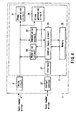
- FIG. 4 shows an internal configuration of LSI;
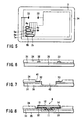
- FIG. 5 shows an antenna substrate;
- FIG. 6 is a sectional view showing the antenna substrate;
- FIG. 7 is a sectional view of the card in which a milling step is completed;
- FIG. 8 is a sectional view of the card in which an implanting step is completed;
- FIG. 9 shows the antenna substrate;
- FIG. 10 is an external view of the card in which the milling-step is completed;
- FIG. 11 shows a state in which a cut portion of a capacitor pattern (signal line) is cut;
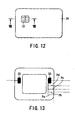
- FIG. 12 is an external view of the card in which the implanting step is completed; and
- FIG. 13 shows a layout example of the cut portion of the capacitor pattern.
- An IC card according to an embodiment of the invention will be described below referring to the accompanying drawings.
- The IC card is a combination-
type IC card 1 which can carry out data communication with a card reader/writer as an external terminal with both contact and contactless (wireless) interfaces. - As shown in FIGS. 1 and 2, the combination-
type IC card 1 has atuning circuit 8 which includes anantenna 3 and tuning capacitors for trimming (pattern capacitor) 4, 5, 6, and 7 in anantenna card 2 and anIC module 9 which is electrically connected to the tuning circuit and is mounted on theantenna card 2. - The IC module 9 a
substrate 10, anLSI 11 which is mounted on thesubstrate 10 by wire bonding, acontact portion 12 which is mounted on the other side of theLSI 11 of thesubstrate 10, and pads forconnection - A resonance circuit includes the
tuning circuit 8 andLSI 11. - The
contact portion 12 includes, e.g. a plurality ofterminals 12a to 12h, which have aVCC terminal 12a for operational power voltage (+5V), anRST terminal 12b for a reset signal, aCLK terminal 12c for a clock signal, a GND terminal 12d for ground, a VPP terminal 12e for write power voltage of memory, an I/O terminal 12f for data input/output, and spareterminals - FIG. 3 is an equivalent circuit of the combination-
type IC card 1 according to the invention. - The resonance circuit is formed by the
antenna 3, thetuning capacitors LSI 11. The combination-type IC card 1 carries out the contactless data communication in such a manner that the combination-type IC card 1 converts radio waves supplied from the outside of the card into electric power to operate theLSI 11 and transmits a response using the remaining electric power. - In the case of the contact data communication, the data communication is carried out through the
contact portion 12. - In the embodiment, the resonance frequency of the combination-
type IC card 1 is turned to a specific frequency. To this end, parts (Pa and Pd) of a pattern (signal line) that connects thecapacitors 4 to 7 to theantenna 3 are cut, changing the capacitance of the resonant circuit and thus achieving trimming. - As shown in FIG. 4, the
LSI 11 includes apower generating circuit 21, ademodulating circuit 22, a control logic circuit 23, a modulatingcircuit 24, amemory 25, aclock generating circuit 26, and aninterface 27. - The
tuning circuit 8 receives a signal of the radio waves from the card reader/writer. Thedemodulating circuit 22 demodulates the received signal to transmit it to the control logic circuit 23, and the control logic circuit 23 carries out command analysis. Then, the control logic circuit 23 writes data in thememory 25 or reads data from thememory 25 according to the contents of the command. The control logic circuit 23 reads the data from thememory 25 to transmit it to the modulatingcircuit 24. The data is modulated with the modulatingcircuit 24 and transmitted to the card reader/writer by the radio waves using thetuning circuit 8. - The
powec generating circuit 21 generates the electric power consumed in thewireless card 1 from the received signal with thetuning circuit 8. - The
clock generating circuit 26 generates a clock required to operate each circuit from the received signal with thetuning circuit 8, and the clock is outputted to thedemodulating circuit 22, the modulatingcircuit 24, and the control logic circuit 23. - Accordingly, the combination-
type IC card 1 carries out the contactless data communication in such a manner that the combination-type IC card 1 converts the radio waves supplied from the outside of the card (card reader/writer) into the electric power to operate theLSI 11 and transmits the response using the remaining electric power. - The
interface 27 is connected to thecontact portion 12, and theinterface 27 carries out exchange of the data between the control logic circuit 23 and the external device (card reader/writer), which is connected to thecontact portion 12 or in contact with thecontact portion 12. - FIG. 5 shows an antenna substrate used in the invention.
- In an
antenna substrate 31, polyethylene terephthalate (hereinafter referred to as PET, not shown) having a thickness of 0.025 mm is used as a base material.Antenna terminals electrodes tuning capacitors antenna 3 and theIC module 9, are formed by etching aluminum foil on one side of theantenna substrate 31. Theother electrodes tuning capacitors antenna substrate 31. - Thus, the
tuning capacitors tuning capacitors - In the embodiment, though the same aluminum foil was used for both sides of the conductor, combinations of copper foil and the aluminum foil or silver paste may be used as the conductor.
- One end of the
antenna 3 is wired to theelectrodes tuning capacitors antenna 3 is wired to theelectrodes tuning capacitors - In the combination-
type IC card 1, in order to carry out trimming to the specific resonance frequency, the tuning capacitors for trimming 4, 5, 6, and 7 are changed by simultaneously cutting their patterns in a milling step. - In a capacitance value of the capacitor for trimming, a correction value is determined by previous measurement in which a probe touches on the
pads IC module 9. - In the embodiment, though the wire bonding is adopted in the mounting method of the
LSI 11, other methods such as a flip-chip method may be adopted. - FIGS. 6 to 8 show a process flow of the combination-
type IC card 1 according to the invention. - In an antenna card 36, as shown in FIGS. 5, 6, and 9, PET sheets or
PVC sheets antenna substrate 31. - The milling is carried out at a predetermined position of the antenna card 36 in order to make
holes IC module 9, and theIC module 9 is implanted in an implanting step to make the combination-type IC card 1. - At this point, the resonance frequency has a value in which the capacitances of the
antenna 3, thetuning capacitors LSI 11 are added. - However, since there are slight variations caused by LSI manufacturing lot and the like in the capacitance of the capacitor inside
LSI 11, its influence causes the resonance frequency to be outside a target value. - The invention proposes a measure which selects and cuts the
tuning capacitors LSI 11 is corrected to establish resonance at the predetermined frequency. - The embodiment will be described in detail below.
- FIGS. 1, 7, and 10 show an external view and a sectional view of the card in which the milling step has been completed. A
shallow bonding hole 41 for bonding theIC module 9 and adeep bonding hole 42 for storing an LSI molding portion are present in the card, while the holes are in the concave form from the surface of the card. The parts (cut portions Pa to Pe) of the pattern connecting theantenna 3 and thecapacitors bonding hole 41 for theIC module 9. In this case, since all thetuning capacitors 
tuning capacitors - However, in the case that it is found from previous inspection that the inner capacitance of the
IC module 9 is larger than an estimated value by (C1+C2), as shown in FIG. 11, the cut portions Pa and Pb of the capacitor pattern (signal line) connected to thetuning capacitors - In the embodiment, the cut portions Pa and Pb of the capacitor pattern are cut with a cutter used in the milling at the same time when the milling step is carried out, so that the dedicated cutter for trimming is not particularly required.
- The pattern may be cut with the cutter for trimming.
- When the cut portion Pe is cut, the capacitances of the
tuning capacitors - As shown in FIG. 1, since the cut portions Pa to Pe of the capacitor pattern are arranged at the side different from the sides where the
antenna connecting terminals antenna connecting terminals IC module 9, there is little fear that the conductive bonding agent overflows and the cut pattern is short-circuited. - Accordingly, this can prevent the risk that the conductive bonding agent overflows and the cut capacitor is connected again in the case that the
antenna connecting terminals - In the embodiment, through the implanting step shown in FIG. 8, the
IC module 9 to which an anisotropic conductive bonding film (not shown) is pre-bonded is dropped into the bonding holes 41 and 42, pressed with heat, and electrically and physically connected to form the combination-type IC card 1 shown in FIG. 12. - The
tuning circuit 8 and theLSI 11 are connected in such a manner that thepads IC module 9 are connected to theantenna connecting terminals - As described above, for example, since the capacitance of the capacitor inside the
LSI 11 slightly has the variation from the manufacturing lot of theLSI 11, its influence causes the resonance frequency to be outside a target resonance frequency f. - In order to correct the variation in the capacitance of the capacitor inside the
LSI 11 to establish resonance at the predetermined frequency, the tuning capacitors for trimming 4, 5, 6, and 7 are selected and connected. As a result, even in the case of the combination-type IC card, a certain communication range can be obtained. - The case in which the variations in the resonance frequencies of a first several LSIs in lot unit are measured and the pattern to be trimmed is determined is described in the embodiment. However, the variation in the resonance frequency of individual LSI may be measured and the pattern to be trimmed may be determined.
- Although the cut portions Ps to Pd of the capacitor pattern are arranged at the side different from the sides where the
antenna connecting terminals antenna connecting terminal - It is explicitly stated that all features disclosed in the description and/or the claims are intended to be disclosed separately and independently from each other for the purpose of original disclosure as well as for the purpose of restricting the claimed invention independent of the compositions of the features in the embodiments and/or the claims. It is explicitly stated that all value ranges or indications of groups of entities disclose every possible intermediate value or intermediate entity for the purpose of original disclosure as well as for the purpose of restricting the claimed invention.
Claims (7)
- A method of mounting a combination-type IC card (1) having a tuning circuit (8) including an antenna (3) and at least one tuning capacitor (4, 5, 6, 7) or trimming in an antenna card (2) and an IC module (9) including LSI (11), which is electrically connected to the tuning circuit (8) and mounted on the antenna card (2), and a contact portion (12) connected to an external device, a resonance circuit including the tuning circuit (8) and LSI (11), comprising:a milling step of making a hole (41) in which the IC module (9) is mounted in the antenna card (2);a trimming step of setting a resonance frequency to various resonance frequencies currently with the milling step by cutting a signal line (Pa - Pd) which connects the tuning capacitor (4, 5, 6, 7) for trimming and the antenna (3); andan implanting step of mounting the IC module (9) into the hole (41) after the trimming step.
- The method according to claim 1, characterized in that the signal line to be trimmed is exposed in forming a rectangular hole (41), in which the IC module (9) is mounted, in the antenna card (2) through the milling step.
- The method according to claim 1, characterized in that the signal line to be cut is exposed at a side different from a side where both end terminals of the antenna (3) are exposed in forming a rectangular hole (41), in which the IC module (9) is mounted, in the antenna card (2) through the milling step.
- The method according to claim 1, characterized in that the signal line to be cut is provided at a position where the signal line is exposed after milling through the milling step.
- A mounting method of a combination-type IC card (1) according to claim 1, characterized in that the trimming step carries out trimming by cutting a part of an exposed pattern exposed after milling through the milling step.
- A combination-type card comprising:an antenna card (1) incorporating an antenna terminal and an LSI (11); andan IC module (9) held in the antenna card (1) and including a contact unit (12) and an antenna-connecting terminal electrically connected to the antenna terminal (32, 33), the contact unit (12) being connected to the LSI (11) and to be connected to an external device,wherein the antenna card (11) comprises a plurality of tuning capacitors (4, 5, 6, 7) connected by signal lines (Pa - Pd) to the antenna terminal (32, 33), the antenna (3) and the tuning capacitors (4, 5, 6, 7) constitute a turning circuit (8), the turning circuit (8) and the LSI (11) constitute a resonant, and a resonance frequency of the resonant circuit is adjusted by cutting at least one of the signal lines (Pa - Pd).
- The combination-type card according to claim 6, characterized in that at least one of the signal lines (Pa - Pd) is cut when a hole (41) is made in the antenna card (1) to hold the IC module (9).
Applications Claiming Priority (2)
| Application Number | Priority Date | Filing Date | Title |
|---|---|---|---|
| JP2002283521 | 2002-09-27 | ||
| JP2002283521A JP2004118694A (en) | 2002-09-27 | 2002-09-27 | Mounting method of combination IC card |
Publications (3)
| Publication Number | Publication Date |
|---|---|
| EP1403816A2 true EP1403816A2 (en) | 2004-03-31 |
| EP1403816A3 EP1403816A3 (en) | 2005-06-15 |
| EP1403816B1 EP1403816B1 (en) | 2008-02-13 |
Family
ID=31973356
Family Applications (1)
| Application Number | Title | Priority Date | Filing Date |
|---|---|---|---|
| EP03020949A Expired - Lifetime EP1403816B1 (en) | 2002-09-27 | 2003-09-16 | Method of mounting a hybrid IC card and hybrid IC card |
Country Status (6)
| Country | Link |
|---|---|
| US (1) | US6867981B2 (en) |
| EP (1) | EP1403816B1 (en) |
| JP (1) | JP2004118694A (en) |
| KR (1) | KR100558108B1 (en) |
| CN (1) | CN1264118C (en) |
| DE (1) | DE60319040D1 (en) |
Cited By (3)
| Publication number | Priority date | Publication date | Assignee | Title |
|---|---|---|---|---|
| JP2011203929A (en) * | 2010-03-25 | 2011-10-13 | Dainippon Printing Co Ltd | Noncontact type data carrier with display function |
| WO2015000818A1 (en) * | 2013-07-03 | 2015-01-08 | Fraunhofer-Gesellschaft zur Förderung der angewandten Forschung e.V. | Device and method for adapting a resonant circuit for a playing device |
| EP3496005A1 (en) * | 2017-12-08 | 2019-06-12 | Gemalto Sa | Method for producing a radiofrequency chip support |
Families Citing this family (49)
| Publication number | Priority date | Publication date | Assignee | Title |
|---|---|---|---|---|
| KR100602621B1 (en) * | 2004-06-16 | 2006-07-19 | 한국조폐공사 | Prefabricated combi card and its manufacturing method |
| US20060000914A1 (en) * | 2004-06-30 | 2006-01-05 | Chen Chien-Yuan | Memory card capable of wireless transmission |
| JP5459956B2 (en) * | 2004-09-16 | 2014-04-02 | サーク・コーポレーション | Contactless card reader integrated with touchpad |
| EP1866881B1 (en) * | 2005-03-09 | 2018-07-18 | Diebold Nixdorf, Incorporated | Check accepting and cash dispensing automated banking machine system and method |
| US8527510B2 (en) | 2005-05-23 | 2013-09-03 | Monster Worldwide, Inc. | Intelligent job matching system and method |
| FR2890212B1 (en) * | 2005-08-30 | 2009-08-21 | Smart Packaging Solutions Sps | ELECTRONIC MODULE WITH A DOUBLE COMMUNICATION INTERFACE, IN PARTICULAR FOR A CHIP CARD |
| JP2007172592A (en) * | 2005-11-25 | 2007-07-05 | Semiconductor Energy Lab Co Ltd | Semiconductor device |
| US8195657B1 (en) | 2006-01-09 | 2012-06-05 | Monster Worldwide, Inc. | Apparatuses, systems and methods for data entry correlation |
| US8600931B1 (en) | 2006-03-31 | 2013-12-03 | Monster Worldwide, Inc. | Apparatuses, methods and systems for automated online data submission |
| US12314907B2 (en) | 2006-03-31 | 2025-05-27 | Monster Worldwide, Inc. | Apparatuses, methods and systems for automated online data submission |
| US7965520B2 (en) * | 2007-01-22 | 2011-06-21 | Sony Ericsson Mobile Communications Ab | Electronic device with flip module having low height |
| US9779390B1 (en) | 2008-04-21 | 2017-10-03 | Monster Worldwide, Inc. | Apparatuses, methods and systems for advancement path benchmarking |
| JP5172762B2 (en) * | 2009-03-27 | 2013-03-27 | リンテック株式会社 | Antenna circuit, IC inlet, IC tag, and capacity adjustment method of antenna circuit |
| US8789762B2 (en) | 2010-08-12 | 2014-07-29 | Feinics Amatech Teoranta | RFID antenna modules and methods of making |
| US8991712B2 (en) | 2010-08-12 | 2015-03-31 | Féinics Amatech Teoranta | Coupling in and to RFID smart cards |
| JP5724313B2 (en) * | 2010-11-16 | 2015-05-27 | セイコーエプソン株式会社 | Wireless communication device |
| CN102024176A (en) * | 2010-12-09 | 2011-04-20 | 武汉天喻信息产业股份有限公司 | Manufacturing method of double-interface smart card |
| CN102328120B (en) * | 2011-09-08 | 2013-04-17 | 张开兰 | Groove milling method for producing IC (Integrated Circuit) intelligent card |
| US9740342B2 (en) | 2011-12-23 | 2017-08-22 | Cirque Corporation | Method for preventing interference of contactless card reader and touch functions when they are physically and logically bound together for improved authentication security |
| CN104169850B (en) | 2012-01-12 | 2017-06-06 | 辛纳普蒂克斯公司 | Single layer capacitive imaging sensor |
| US9262651B2 (en) | 2013-01-08 | 2016-02-16 | Cirque Corporation | Method for preventing unintended contactless interaction when performing contact interaction |
| US9542023B2 (en) | 2013-08-07 | 2017-01-10 | Synaptics Incorporated | Capacitive sensing using matrix electrodes driven by routing traces disposed in a source line layer |
| US9298325B2 (en) | 2013-09-30 | 2016-03-29 | Synaptics Incorporated | Processing system for a capacitive sensing device |
| US10042489B2 (en) | 2013-09-30 | 2018-08-07 | Synaptics Incorporated | Matrix sensor for image touch sensing |
| US20150091842A1 (en) | 2013-09-30 | 2015-04-02 | Synaptics Incorporated | Matrix sensor for image touch sensing |
| US9459367B2 (en) | 2013-10-02 | 2016-10-04 | Synaptics Incorporated | Capacitive sensor driving technique that enables hybrid sensing or equalization |
| US9274662B2 (en) | 2013-10-18 | 2016-03-01 | Synaptics Incorporated | Sensor matrix pad for performing multiple capacitive sensing techniques |
| US9081457B2 (en) | 2013-10-30 | 2015-07-14 | Synaptics Incorporated | Single-layer muti-touch capacitive imaging sensor |
| US9798429B2 (en) | 2014-02-28 | 2017-10-24 | Synaptics Incorporated | Guard electrodes in a sensing stack |
| KR101762778B1 (en) | 2014-03-04 | 2017-07-28 | 엘지이노텍 주식회사 | Wireless communication and charge substrate and wireless communication and charge device |
| US10133421B2 (en) | 2014-04-02 | 2018-11-20 | Synaptics Incorporated | Display stackups for matrix sensor |
| US9836682B2 (en) | 2014-04-07 | 2017-12-05 | American Banknote Corporation | System and method for detecting the depth of an antenna in the card body of a smart card |
| US9927832B2 (en) | 2014-04-25 | 2018-03-27 | Synaptics Incorporated | Input device having a reduced border region |
| US20170330153A1 (en) | 2014-05-13 | 2017-11-16 | Monster Worldwide, Inc. | Search Extraction Matching, Draw Attention-Fit Modality, Application Morphing, and Informed Apply Apparatuses, Methods and Systems |
| US9690397B2 (en) | 2014-05-20 | 2017-06-27 | Synaptics Incorporated | System and method for detecting an active pen with a matrix sensor |
| US10175827B2 (en) | 2014-12-23 | 2019-01-08 | Synaptics Incorporated | Detecting an active pen using a capacitive sensing device |
| US9778713B2 (en) | 2015-01-05 | 2017-10-03 | Synaptics Incorporated | Modulating a reference voltage to preform capacitive sensing |
| CN106157019A (en) * | 2015-03-26 | 2016-11-23 | 咏嘉科技股份有限公司 | Nfc payment module and control method thereof |
| US9939972B2 (en) | 2015-04-06 | 2018-04-10 | Synaptics Incorporated | Matrix sensor with via routing |
| USD776664S1 (en) * | 2015-05-20 | 2017-01-17 | Chaya Coleena Hendrick | Smart card |
| US9720541B2 (en) | 2015-06-30 | 2017-08-01 | Synaptics Incorporated | Arrangement of sensor pads and display driver pads for input device |
| US9715304B2 (en) | 2015-06-30 | 2017-07-25 | Synaptics Incorporated | Regular via pattern for sensor-based input device |
| US10095948B2 (en) | 2015-06-30 | 2018-10-09 | Synaptics Incorporated | Modulation scheme for fingerprint sensing |
| CN205028263U (en) | 2015-09-07 | 2016-02-10 | 辛纳普蒂克斯公司 | Capacitance sensor |
| US10037112B2 (en) | 2015-09-30 | 2018-07-31 | Synaptics Incorporated | Sensing an active device'S transmission using timing interleaved with display updates |
| US10067587B2 (en) | 2015-12-29 | 2018-09-04 | Synaptics Incorporated | Routing conductors in an integrated display device and sensing device |
| CN106933400B (en) | 2015-12-31 | 2021-10-29 | 辛纳普蒂克斯公司 | Single-layer sensor pattern and sensing method |
| US10909436B2 (en) * | 2019-05-13 | 2021-02-02 | American Express Travel Related Services Company, Inc. | Angled slot in a transaction card |
| US10977539B1 (en) | 2019-12-20 | 2021-04-13 | Capital One Services, Llc | Systems and methods for use of capacitive member to prevent chip fraud |
Family Cites Families (8)
| Publication number | Priority date | Publication date | Assignee | Title |
|---|---|---|---|---|
| SE450057B (en) * | 1984-11-20 | 1987-06-01 | Saab Automation Ab | IDENTITY ISSUES FOR IDENTIFICATION OF FORMAL |
| FR2716281B1 (en) * | 1994-02-14 | 1996-05-03 | Gemplus Card Int | Method of manufacturing a contactless card. |
| JP3064840B2 (en) | 1994-12-22 | 2000-07-12 | ソニー株式会社 | IC card |
| ES2145461T3 (en) * | 1996-07-15 | 2000-07-01 | Austria Card | DATA SUPPORT PRESENTED BY A MODULE AND A HOLOGRAM. |
| JPH1092690A (en) * | 1996-09-18 | 1998-04-10 | Kokusai Electric Co Ltd | Capacity adjustment device |
| IL122250A (en) * | 1997-11-19 | 2003-07-31 | On Track Innovations Ltd | Smart card amenable to assembly using two manufacturing stages and a method of manufacture thereof |
| JP4242512B2 (en) * | 1999-05-20 | 2009-03-25 | 凸版印刷株式会社 | Tuning adjustment method for non-contact IC card |
| FR2808648B1 (en) * | 2000-05-03 | 2004-07-30 | Schlumberger Systems & Service | ANTENNA FOR AN INTEGRATED CIRCUIT CARD AND METHOD FOR ADJUSTING THE INDUCTANCE OF SUCH AN ANTENNA |
-
2002
- 2002-09-27 JP JP2002283521A patent/JP2004118694A/en not_active Abandoned
-
2003
- 2003-09-16 EP EP03020949A patent/EP1403816B1/en not_active Expired - Lifetime
- 2003-09-16 DE DE60319040T patent/DE60319040D1/en not_active Expired - Lifetime
- 2003-09-22 KR KR1020030065506A patent/KR100558108B1/en not_active Expired - Fee Related
- 2003-09-22 US US10/665,420 patent/US6867981B2/en not_active Expired - Fee Related
- 2003-09-26 CN CNB031598927A patent/CN1264118C/en not_active Expired - Fee Related
Cited By (4)
| Publication number | Priority date | Publication date | Assignee | Title |
|---|---|---|---|---|
| JP2011203929A (en) * | 2010-03-25 | 2011-10-13 | Dainippon Printing Co Ltd | Noncontact type data carrier with display function |
| WO2015000818A1 (en) * | 2013-07-03 | 2015-01-08 | Fraunhofer-Gesellschaft zur Förderung der angewandten Forschung e.V. | Device and method for adapting a resonant circuit for a playing device |
| EP3496005A1 (en) * | 2017-12-08 | 2019-06-12 | Gemalto Sa | Method for producing a radiofrequency chip support |
| WO2019110437A1 (en) | 2017-12-08 | 2019-06-13 | Gemalto Sa | Method for producing a radiofrequency chip support |
Also Published As
| Publication number | Publication date |
|---|---|
| EP1403816B1 (en) | 2008-02-13 |
| KR100558108B1 (en) | 2006-03-10 |
| CN1264118C (en) | 2006-07-12 |
| DE60319040D1 (en) | 2008-03-27 |
| US6867981B2 (en) | 2005-03-15 |
| CN1492378A (en) | 2004-04-28 |
| KR20040027357A (en) | 2004-04-01 |
| EP1403816A3 (en) | 2005-06-15 |
| JP2004118694A (en) | 2004-04-15 |
| US20040062012A1 (en) | 2004-04-01 |
Similar Documents
| Publication | Publication Date | Title |
|---|---|---|
| EP1403816B1 (en) | Method of mounting a hybrid IC card and hybrid IC card | |
| JP7539317B2 (en) | RFID strap having top and bottom conductors - Patents.com | |
| US8960561B2 (en) | Wireless communication device | |
| JP4052111B2 (en) | Wireless information storage medium | |
| US6614398B2 (en) | Antenna structure and communication apparatus including the same | |
| US6900536B1 (en) | Method for producing an electrical circuit | |
| EP3295512B1 (en) | Rifd tag with a tunable antenna | |
| CN101233532B (en) | Antenna structure, transponder and method of manufacturing an antenna structure | |
| EP1538560A2 (en) | Antenna for radio frequency identification | |
| US20090014527A1 (en) | Ask-026 | |
| CN100412898C (en) | radio frequency identification tag | |
| JP2019505891A (en) | Radio frequency device with tunable LC circuit with electrical and / or electronic modules | |
| CN105408918A (en) | RFID tags, and RFID systems | |
| JP4016261B2 (en) | RFID transponder and method for adjusting resonance frequency | |
| US20030016506A1 (en) | Non-contact type IC card and flat coil used for the same | |
| JPH11353440A (en) | Capacitors and contactless IC cards | |
| JP2003249814A (en) | Loop antenna with tuning capacitor for non-contact RFID tag | |
| JP4661833B2 (en) | Non-contact type IC module and method of manufacturing non-contact type IC module | |
| US7800200B2 (en) | Wireless IC tag and method for manufacturing same | |
| JP4242512B2 (en) | Tuning adjustment method for non-contact IC card | |
| JP2004078768A (en) | Non-contact IC card mounting method | |
| JP2001357369A (en) | IC chips for mounting IC cards, etc. | |
| JP4453730B2 (en) | RFID tag manufacturing method | |
| JP4048652B2 (en) | IC card and manufacturing method thereof | |
| JP2007233703A (en) | Wireless tag and its manufacturing method |
Legal Events
| Date | Code | Title | Description |
|---|---|---|---|
| PUAI | Public reference made under article 153(3) epc to a published international application that has entered the european phase |
Free format text: ORIGINAL CODE: 0009012 |
|
| 17P | Request for examination filed |
Effective date: 20030916 |
|
| AK | Designated contracting states |
Kind code of ref document: A2 Designated state(s): AT BE BG CH CY CZ DE DK EE ES FI FR GB GR HU IE IT LI LU MC NL PT RO SE SI SK TR |
|
| AX | Request for extension of the european patent |
Extension state: AL LT LV MK |
|
| PUAL | Search report despatched |
Free format text: ORIGINAL CODE: 0009013 |
|
| AK | Designated contracting states |
Kind code of ref document: A3 Designated state(s): AT BE BG CH CY CZ DE DK EE ES FI FR GB GR HU IE IT LI LU MC NL PT RO SE SI SK TR |
|
| AX | Request for extension of the european patent |
Extension state: AL LT LV MK |
|
| AKX | Designation fees paid |
Designated state(s): DE FR GB |
|
| GRAP | Despatch of communication of intention to grant a patent |
Free format text: ORIGINAL CODE: EPIDOSNIGR1 |
|
| GRAA | (expected) grant |
Free format text: ORIGINAL CODE: 0009210 |
|
| GRAS | Grant fee paid |
Free format text: ORIGINAL CODE: EPIDOSNIGR3 |
|
| AK | Designated contracting states |
Kind code of ref document: B1 Designated state(s): DE FR GB |
|
| REG | Reference to a national code |
Ref country code: GB Ref legal event code: FG4D |
|
| REF | Corresponds to: |
Ref document number: 60319040 Country of ref document: DE Date of ref document: 20080327 Kind code of ref document: P |
|
| ET | Fr: translation filed | ||
| PLBE | No opposition filed within time limit |
Free format text: ORIGINAL CODE: 0009261 |
|
| STAA | Information on the status of an ep patent application or granted ep patent |
Free format text: STATUS: NO OPPOSITION FILED WITHIN TIME LIMIT |
|
| 26N | No opposition filed |
Effective date: 20081114 |
|
| PG25 | Lapsed in a contracting state [announced via postgrant information from national office to epo] |
Ref country code: DE Free format text: LAPSE BECAUSE OF FAILURE TO SUBMIT A TRANSLATION OF THE DESCRIPTION OR TO PAY THE FEE WITHIN THE PRESCRIBED TIME-LIMIT Effective date: 20080514 |
|
| GBPC | Gb: european patent ceased through non-payment of renewal fee |
Effective date: 20080916 |
|
| PG25 | Lapsed in a contracting state [announced via postgrant information from national office to epo] |
Ref country code: GB Free format text: LAPSE BECAUSE OF NON-PAYMENT OF DUE FEES Effective date: 20080916 |
|
| PGFP | Annual fee paid to national office [announced via postgrant information from national office to epo] |
Ref country code: FR Payment date: 20140906 Year of fee payment: 12 |
|
| REG | Reference to a national code |
Ref country code: FR Ref legal event code: ST Effective date: 20160531 |
|
| PG25 | Lapsed in a contracting state [announced via postgrant information from national office to epo] |
Ref country code: FR Free format text: LAPSE BECAUSE OF NON-PAYMENT OF DUE FEES Effective date: 20150930 |