JP5724313B2 - Wireless communication device - Google Patents
Wireless communication device Download PDFInfo
- Publication number
- JP5724313B2 JP5724313B2 JP2010255596A JP2010255596A JP5724313B2 JP 5724313 B2 JP5724313 B2 JP 5724313B2 JP 2010255596 A JP2010255596 A JP 2010255596A JP 2010255596 A JP2010255596 A JP 2010255596A JP 5724313 B2 JP5724313 B2 JP 5724313B2
- Authority
- JP
- Japan
- Prior art keywords
- wireless communication
- circuit board
- antenna
- communication device
- communication apparatus
- Prior art date
- Legal status (The legal status is an assumption and is not a legal conclusion. Google has not performed a legal analysis and makes no representation as to the accuracy of the status listed.)
- Expired - Fee Related
Links
Images


Classifications
-
- H—ELECTRICITY
- H01—ELECTRIC ELEMENTS
- H01Q—ANTENNAS, i.e. RADIO AERIALS
- H01Q1/00—Details of, or arrangements associated with, antennas
- H01Q1/36—Structural form of radiating elements, e.g. cone, spiral, umbrella; Particular materials used therewith
-
- G—PHYSICS
- G04—HOROLOGY
- G04G—ELECTRONIC TIME-PIECES
- G04G17/00—Structural details; Housings
- G04G17/02—Component assemblies
- G04G17/04—Mounting of electronic components
-
- G—PHYSICS
- G04—HOROLOGY
- G04G—ELECTRONIC TIME-PIECES
- G04G17/00—Structural details; Housings
- G04G17/02—Component assemblies
- G04G17/06—Electric connectors, e.g. conductive elastomers
-
- G—PHYSICS
- G04—HOROLOGY
- G04G—ELECTRONIC TIME-PIECES
- G04G21/00—Input or output devices integrated in time-pieces
- G04G21/04—Input or output devices integrated in time-pieces using radio waves
-
- H—ELECTRICITY
- H01—ELECTRIC ELEMENTS
- H01Q—ANTENNAS, i.e. RADIO AERIALS
- H01Q1/00—Details of, or arrangements associated with, antennas
- H01Q1/27—Adaptation for use in or on movable bodies
- H01Q1/273—Adaptation for carrying or wearing by persons or animals
-
- H—ELECTRICITY
- H01—ELECTRIC ELEMENTS
- H01Q—ANTENNAS, i.e. RADIO AERIALS
- H01Q9/00—Electrically-short antennas having dimensions not more than twice the operating wavelength and consisting of conductive active radiating elements
- H01Q9/04—Resonant antennas
- H01Q9/16—Resonant antennas with feed intermediate between the extremities of the antenna, e.g. centre-fed dipole
-
- H—ELECTRICITY
- H04—ELECTRIC COMMUNICATION TECHNIQUE
- H04B—TRANSMISSION
- H04B1/00—Details of transmission systems, not covered by a single one of groups H04B3/00 - H04B13/00; Details of transmission systems not characterised by the medium used for transmission
- H04B1/38—Transceivers, i.e. devices in which transmitter and receiver form a structural unit and in which at least one part is used for functions of transmitting and receiving
- H04B1/3827—Portable transceivers
- H04B1/385—Transceivers carried on the body, e.g. in helmets
Description
本発明は、無線通信装置に関するものである。 The present invention relates to a wireless communication apparatus.
近年、無線通信装置の小型化が進み腕時計タイプのものも出現している。小型・軽量化のための高密度実装が必須であるとともに、厳しい受信環境の下、受信感度の向上のためアンテナ構造が重要である。例えば、小型無線通信装置のアンテナを設置する構造が示されている(例えば、特許文献1参照)。 In recent years, a wireless communication device has been miniaturized and a wristwatch type has also appeared. High-density mounting is indispensable for miniaturization and weight reduction, and an antenna structure is important for improving reception sensitivity under severe reception environments. For example, a structure for installing an antenna of a small wireless communication device is shown (see, for example, Patent Document 1).
しかしながら、特許文献1の構造では、チップアンテナ等のアンテナ素子が必要な上、高周波回路とアンテナとの接続手段が必要となり、小型・軽量化、及び低コスト化が困難になる虞がある。 However, the structure of Patent Document 1 requires an antenna element such as a chip antenna and requires a connection means between the high-frequency circuit and the antenna, which may make it difficult to reduce the size, weight, and cost.
本発明は、上述の課題の少なくとも一部を解決するためになされたものであり、以下の形態又は適用例として実現することが可能である。 SUMMARY An advantage of some aspects of the invention is to solve at least a part of the problems described above, and the invention can be implemented as the following forms or application examples.
[適用例1]複数の第1端子部が設置される第1回路基板と、前記第1回路基板上に設置され、前記複数の第1端子部のうち少なくとも1つに接続される高周波回路と、前記複数の第1端子部と対向する複数の第2端子部が設置される第2回路基板と、前記第2回路基板上に設置され、前記複数の第2端子部のうち少なくとも1つに接続される第1内部回路と、前記複数の第1端子部と前記複数の第2端子部とを導通する導通手段と、を含み、前記複数の第1端子部及び前記複数の第2端子部のうち少なくとも一方の前記高周波回路に接続される端子を含む少なくとも2つの連続する端子間は、コンデンサーを介して接続され、前記複数の第1端子部及び前記複数の第2端子部のうち少なくとも一方の少なくとも1つの連続する端子間は、無線通信用のアンテナとして機能することを特徴とする無線通信装置。 Application Example 1 A first circuit board on which a plurality of first terminal portions are installed, a high-frequency circuit that is installed on the first circuit board and connected to at least one of the plurality of first terminal portions, A second circuit board on which a plurality of second terminal parts facing the plurality of first terminal parts are installed; and at least one of the plurality of second terminal parts installed on the second circuit board. A plurality of first terminal portions and a plurality of second terminal portions, comprising: a first internal circuit to be connected; and a conduction means for conducting the plurality of first terminal portions and the plurality of second terminal portions. Between at least two continuous terminals including a terminal connected to at least one of the high-frequency circuits is connected via a capacitor, and at least one of the plurality of first terminal portions and the plurality of second terminal portions. Between at least one continuous terminal Radio communication apparatus characterized by functioning as an antenna for communication.
これによれば、小型無線通信装置において、導通手段と接続される複数の第1端子部及び複数の第2端子部のうち少なくとも一方の少なくとも1つの連続する端子間をアンテナとして使用するので、チップアンテナ等のアンテナ素子が不要となる上、アンテナ接続手段も不要となるため、機器の小型・軽量化・低コストが可能となる。 According to this, in the small wireless communication device, since at least one continuous terminal of at least one of the plurality of first terminal portions and the plurality of second terminal portions connected to the conduction unit is used as an antenna, the chip Since an antenna element such as an antenna is not required and an antenna connection means is not required, the apparatus can be reduced in size, weight, and cost.
[適用例2]上記無線通信装置であって、前記導通手段の少なくとも一部は、無線通信用のアンテナとして機能することを特徴とする無線通信装置。 Application Example 2 In the above wireless communication device, at least a part of the conduction means functions as an antenna for wireless communication.
これによれば、一般に導通手段は第1回路基板外周部に設置されている。この位置は自由空間に近く、またノイズ源となるCPU等のICから離れる。したがって、これをアンテナとして機能するように使用した場合、アンテナ性能がさらに向上する。 According to this, the conduction means is generally installed on the outer periphery of the first circuit board. This position is close to free space and away from an IC such as a CPU that becomes a noise source. Therefore, when this is used so as to function as an antenna, the antenna performance is further improved.
[適用例3]上記無線通信装置であって、前記複数の第1端子部は、前記第1回路基板の上下又は左右に設置されていることを特徴とする無線通信装置。 Application Example 3 In the above wireless communication device, the plurality of first terminal portions are installed on the top and bottom or the left and right of the first circuit board.
これによれば、高性能なアンテナ構成を選択することにより、高周波回路の送信効率及び受信感度が向上する。 According to this, by selecting a high-performance antenna configuration, the transmission efficiency and the reception sensitivity of the high-frequency circuit are improved.
[適用例4]上記無線通信装置であって、前記無線通信用のアンテナとして機能する構成は、ダイポールアンテナであることを特徴とする無線通信装置。 Application Example 4 In the wireless communication device, the configuration that functions as the antenna for wireless communication is a dipole antenna.
これによれば、高性能なアンテナ素子となるので高周波回路の送信効率、受信感度が向上する。モノポールアンテナでは、その性能を発揮させるためには大面積のGNDが必要であるが、腕時計タイプのような小型無線通信装置では十分に確保することが困難である。一方、ダイポールアンテナは原理的にGNDを必要としないため腕時計タイプのような小型無線通信装置においては好適である。 According to this, since it becomes a high-performance antenna element, the transmission efficiency and reception sensitivity of the high-frequency circuit are improved. A monopole antenna requires a large-area GND in order to exhibit its performance, but it is difficult to sufficiently secure it with a small wireless communication device such as a wristwatch type. On the other hand, since a dipole antenna does not require GND in principle, it is suitable for a small wireless communication apparatus such as a wristwatch type.
[適用例5]上記無線通信装置であって、前記無線通信用のアンテナとして機能する構成は、ダイバーシティーアンテナであることを特徴とする無線通信装置。 Application Example 5 In the wireless communication apparatus, the configuration that functions as the antenna for wireless communication is a diversity antenna.
これによれば、受信状態の良い方のアンテナ素子を選択できるため、高性能なアンテナ素子となり高周波回路の送信効率、受信感度が向上する。 According to this, since the antenna element with the better reception state can be selected, it becomes a high-performance antenna element and the transmission efficiency and reception sensitivity of the high-frequency circuit are improved.
[適用例6]上記無線通信装置であって、前記第1回路基板上に設置され、前記複数の第1端子部のうち少なくとも1つに接続され、直流信号又は低周波信号が出力される第2内部回路を含み、一端が前記第2端子部に接続され、他端が前記第1内部回路に接続される第1高周波遮断素子と、一端が前記第1端子部に接続され、他端が前記第2内部回路に接続される第2高周波遮断素子と、の少なくとも一方をさらに含むことを特徴とする無線通信装置。 Application Example 6 In the wireless communication device described above, the wireless communication device is installed on the first circuit board, connected to at least one of the plurality of first terminal portions, and outputs a DC signal or a low-frequency signal. Including one internal circuit, one end connected to the second terminal portion, the other end connected to the first internal circuit, one end connected to the first terminal portion, and the other end The wireless communication apparatus further comprising at least one of a second high-frequency cutoff element connected to the second internal circuit.
これによれば、高周波回路とアンテナ機能とは、第1高周波遮断素子を介して第1内部回路と接続された第2回路基板の面にある第2端子部を介して接続されるため、第1内部回路に入力される信号の直流信号又は低周波信号と、高周波回路に使用される高周波信号と、は周波数で分離される。また、高周波回路とアンテナ機能とは、第2高周波遮断素子を介して第2内部回路と接続された第1回路基板の面にある第1端子部を介して接続されるため、第2内部回路に入力される信号の直流信号又は低周波信号と、高周波回路に使用される高周波信号と、は周波数で分離される。 According to this, since the high-frequency circuit and the antenna function are connected via the second terminal portion on the surface of the second circuit board connected to the first internal circuit via the first high-frequency cutoff element, 1 A DC signal or low-frequency signal of a signal input to the internal circuit and a high-frequency signal used in the high-frequency circuit are separated by frequency. Further, since the high frequency circuit and the antenna function are connected via the first terminal portion on the surface of the first circuit board connected to the second internal circuit via the second high frequency cutoff element, the second internal circuit The DC signal or low frequency signal of the signal input to the signal is separated from the high frequency signal used in the high frequency circuit.
[適用例7]上記無線通信装置であって、前記第1及び第2高周波遮断素子は、インダクタンス素子であることを特徴とする無線通信装置。 Application Example 7 In the wireless communication apparatus, the first and second high frequency cutoff elements are inductance elements.
これによれば、インダクタンス素子がいわゆるローパスフィルターの働きをする。すなわち、高周波信号の周波数成分に対しては高インピーダンスとなり、直流信号又は低周波信号の周波数成分に対しては低インピーダンスとなるので、第1及び第2内部回路への高周波信号の漏洩を防止することができるとともに、第1及び第2端子部に印加された直流信号又は低周波信号を第1及び第2内部回路へ流すことができる。 According to this, the inductance element functions as a so-called low-pass filter. That is, since it has a high impedance for the frequency component of the high frequency signal and a low impedance for the frequency component of the DC signal or the low frequency signal, the leakage of the high frequency signal to the first and second internal circuits is prevented. In addition, a DC signal or a low-frequency signal applied to the first and second terminal portions can be passed to the first and second internal circuits.
[適用例8]上記無線通信装置であって、前記第1及び第2高周波遮断素子は、抵抗素子であることを特徴とする無線通信装置。 Application Example 8 In the wireless communication apparatus, the first and second high frequency cutoff elements are resistance elements.
これによれば、抵抗素子は、高周波信号(電流量大)を遮断する機能を有している。また、第1及び第2内部回路に流れる電流は微小であるから、ある程度の抵抗値は許容できるため、第1及び第2端子部に印加された直流信号又は低周波信号を第1及び第2内部回路へ流すことができる。 According to this, the resistance element has a function of blocking a high-frequency signal (a large amount of current). Further, since the current flowing through the first and second internal circuits is very small, a certain resistance value can be allowed. Therefore, the direct current signal or the low frequency signal applied to the first and second terminal portions can be used as the first and second frequency signals. Can flow to internal circuit.
[適用例9]上記無線通信装置であって、前記第1内部回路は、表示部であり、前記第2内部回路は、信号処理用のデジタルICであることを特徴とする無線通信装置。 Application Example 9 In the wireless communication apparatus, the first internal circuit is a display unit, and the second internal circuit is a digital IC for signal processing.
これによれば、無線通信装置内の情報を目視確認及びデジタル信号処理することができる。 According to this, the information in the wireless communication device can be visually confirmed and digital signal processed.
図面に基づいて、本実施形態に係る無線通信装置としての腕装着型無線通信装置を説明する。 Based on the drawings, an arm-mounted wireless communication device as a wireless communication device according to the present embodiment will be described.
(第1の実施形態)
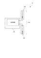
図1は、本実施形態に係る腕装着型無線通信装置の全体構成を示す説明図である。図2は、本実施形態に係る腕装着型無線通信装置に搭載された回路組立体を示す平面図及び底面図である。
(First embodiment)
FIG. 1 is an explanatory diagram showing the overall configuration of the wrist-worn radio communication apparatus according to the present embodiment. 2A and 2B are a plan view and a bottom view showing the circuit assembly mounted on the arm-mounted radio communication device according to the present embodiment.
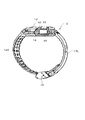
本実施形態に係る腕装着型無線通信装置2は、液晶表示パネル(表示部)(第1内部回路)10が配置されている側が表面側とされる装置本体12と、一対の腕バンド14R,14Lとから構成されている。それぞれの腕バンド14R,14Lは、各バンド基端が装置本体12の両端に取り付けられており、これらのバンドは、各末端部で尾錠16によって相互に結合することが可能になっている。
The arm-mounted
装置本体12は、表面側のケーシング18と、装置本体12の裏側でケーシング18の裏側に固定される裏カバー20とで構成されている。ケーシング18と裏カバー20とによって構成された装置本体12には、回路組立体22が内蔵されている。回路組立体22は、その主要構成部品が、装置本体12の内部においてその厚さ方向に積層配置された構造になっている。すなわち、回路組立体22では、図2に示すように、液晶表示パネル10と、回路基板(第1回路基板)24と、回路駆動用電池26とが厚さ方向に配置されている。
The apparatus
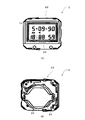
図3は、本実施形態に係る腕装着型無線通信装置2の上面図である。腕装着型無線通信装置2は、回路基板24と、表示パネル基板(第2回路基板)32と、を備えている。回路基板24上には、後述する種々の集積回路(IC:Integrated Circuit)と、回路基板側端子と、が配置されている。回路基板24には、多層基板が用いられ、ガラス−エポキシ基板やフェノール樹脂基板やセラミック基板からなる基板に表層パターン(配線パターン)が形成されている。
FIG. 3 is a top view of the arm-mounted
表示パネル基板32上には、液晶表示パネル10と、後述する表示パネル側端子と、が配置されている。
On the
一般に、回路基板24上の回路基板側端子と表示パネル基板32上の表示パネル側端子とは、「導体に金属粒子を使用した導電シリコーンゴムと電気絶縁性シリコーンゴムをゼブラ状に交互に積層したゴムコネクター」(通称ゼブラ、以下ゼブラコネクター(導電手段)と称す)により接続されている。ここで、液晶表示パネル10に供給される信号は直流信号又は低周波数(1MHz以下)の信号であるから、現在通常無線通信に使用される例えば周波数2.4GHzの高周波信号と分離させることができる。
In general, the circuit board side terminal on the
図4は、本実施形態に係る腕装着型無線通信装置2の上面図である。尚、図4は、回路基板24から表示パネル基板32を外した状態である。回路基板24には、送信及び受信の機能を備える高周波アナログIC36と、回路基板側端子28と、高周波アナログIC36と回路基板側端子28とを接続する配線52とが配置されている。高周波アナログIC36は、例えば2.4GHzといった高周波信号(RF信号)を送受信する。
FIG. 4 is a top view of the arm-mounted
回路基板側端子28は、回路基板24と表示パネル基板32との接続用端子として機能する他に、腕装着型無線通信装置2のアンテナとして機能する。複数の回路基板側端子28は、それぞれ違った信号を伝送するため、当然分離されている。したがって、そのままではアンテナとして機能しない。そこで、複数の回路基板側端子28に小容量の結合コンデンサー68を接続する。つまり、高周波的に接続する。一方、回路基板側端子28にかかる信号は、直流信号又は低周波数の信号であるから小容量の結合コンデンサー68で結合しても機能的に問題の発生する虞はない。また、複数の回路基板側端子28に接続する結合コンデンサー68の個数でアンテナ長、つまり周波数を調整できる。
The circuit
一般に回路基板側端子28は回路基板24外周部に設置されている。この位置は自由空間に近く、またノイズ源となるCPU等のICから離れている。したがって、これをアンテナとして使用した場合、アンテナ性能が向上する。
In general, the circuit board-
図5は、本実施形態に係る腕装着型無線通信装置2の上面図である。図5は、回路基板24から表示パネル基板32を外した状態である。回路基板24には、信号処理用デジタルIC(第2内部回路)38が配置されている。信号処理用デジタルIC38は、アナログ/デジタル変換前に受信信号をサンプリングするデジタル回路やフェイズ・ロック・ループ回路などが組み込まれている。
FIG. 5 is a top view of the arm-mounted
信号処理用デジタルIC38への高周波信号の漏洩を確実に防止するため、高周波アナログIC36から見て、回路基板24上の信号処理用デジタルIC38のインピーダンスが低い場合やラインが長い場合には、信号処理用デジタルIC38と回路基板側端子28との間に第2高周波遮断素子としてのインダクタンス素子46あるいは抵抗素子48を挿入してもよい。信号処理用デジタルIC38に供給される信号は、直流信号又は低周波数の信号であり、また電流も微小であるからインダクタンス素子46や抵抗素子48を挿入してもほとんど問題の発生する虞はない。
In order to surely prevent leakage of the high frequency signal to the signal processing
また、本実施形態は、ゼブラコネクターを介して高周波信号が表示パネル基板32へ漏洩する虞があるため、ゼブラコネクターを高抵抗にするかインダクタンス特性を持たせることが望ましい。この場合も、液晶表示パネル10に供給される信号は、直流信号又は低周波数の信号であり、また電流も微小であるからほとんど問題の発生する虞はない。
Further, in the present embodiment, since there is a possibility that a high frequency signal leaks to the
本実施形態によれば、腕装着型無線通信装置2において、複数の回路基板側端子28のうち少なくとも1つの連続する端子間をアンテナとして使用するので、チップアンテナ等のアンテナ素子が不要となる上、アンテナ接続手段も不要となるため、機器の小型・軽量化・低コストが可能となる。
According to the present embodiment, the arm-mounted
(第2の実施形態)
図6は、本実施形態に係る腕装着型無線通信装置の上面図及び断面図である。図6(A)は上面図であり、図6(B)は断面図であり、図6(C)は容量結合を示す図である。尚、図6は、回路基板24から表示パネル基板32を外した状態である。また本実施形態の説明において、前述の実施形態と同一の構成については同一の符号を付し、その説明を省略する。
(Second Embodiment)
FIG. 6 is a top view and a cross-sectional view of the arm-mounted wireless communication apparatus according to the present embodiment. 6A is a top view, FIG. 6B is a cross-sectional view, and FIG. 6C is a diagram showing capacitive coupling. FIG. 6 shows a state where the
本実施形態に係る腕装着型無線通信装置4は、図6(A)に示すように、前述の腕装着型無線通信装置2の結合コンデンサー68に換えて、回路基板側端子28の対向する部分の回路基板24の外層(あるいは内層)にパターン(導体)64を設けている。これにより、図6(C)に示すように、回路基板側端子28間を容量結合させることにより、回路基板側端子28をアンテナとして機能させる。
As shown in FIG. 6A, the arm-mounted
ここで、結合容量について説明する。平板コンデンサーの容量は、C=ε×ε0×S/dである。ここで、εは比誘電率、ε0は真空中の誘電率、Sは回路基板側端子28の面積、dは回路基板側端子28とパターン64との距離である。回路基板24に高誘電率基板を使用して、εが30、Sが0.4mm2(長さ2mm、幅0.2mm)、dが0.01mmとすると、容量は約10.6pFとなる。この場合、2.4GHzのインピーダンスはZ=1/jωCである。ここで、ωは角周波数で、コンデンサー1個当たり約6オームで回路基板側端子28間は約12オームとなり十分な低インピーダンスで接続できる。この容量により複数の回路基板側端子28を高周波的に接続する。
Here, the coupling capacitance will be described. The capacity of the plate capacitor is C = ε × ε 0 × S / d. Here, ε is a relative dielectric constant, ε 0 is a dielectric constant in vacuum, S is an area of the circuit
一方、回路基板側端子28にかかる信号は、直流信号又は低周波数の信号であるからこの程度の容量で結合しても問題の発生する虞はない。例えば、周波数が1MHzとすると1個当たりのインピーダンスは約15Mオームで回路基板側端子28間は約30Mオームとなりほぼオープンと見なせる。
On the other hand, since the signal applied to the circuit
また、パターン64の長さでアンテナ長、つまり周波数を調整することができる。例えば、2.4GHzの真空中の波長λは、12.5cmである。モノポールアンテナの必要長は、λ/4であるため、3.125cmである。ここで例えば、ガラスエポキシ基板を使用した場合、比誘電率εrは4.7として、アンテナの必要長は3.125÷4.7^(1/2)で1.44cmとなる。また例えば、高誘電率セラミック基板を使用した場合、比誘電率εrは30として、アンテナの必要長は3.125÷30^(1/2)で0.57cmとなる。
Further, the antenna length, that is, the frequency can be adjusted by the length of the
本実施形態によれば、コンデンサーを実装する必要がないため、さらに装置の小型・軽量化・低コストが可能となる。 According to this embodiment, since it is not necessary to mount a capacitor, the apparatus can be further reduced in size, weight, and cost.
(第3の実施形態)
図7は、本実施形態に係る腕装着型無線通信装置の断面図である。本実施形態の説明において、前述の実施形態と同一の構成については同一の符号を付し、その説明を省略する。
(Third embodiment)
FIG. 7 is a cross-sectional view of the arm-mounted wireless communication apparatus according to the present embodiment. In the description of this embodiment, the same components as those of the above-described embodiment are denoted by the same reference numerals, and the description thereof is omitted.
本実施形態に係る腕装着型無線通信装置4は、回路基板24上の回路基板側端子28と表示パネル基板32上の表示パネル側端子40とを接続するゼブラコネクター42が配置されている。腕装着型無線通信装置4は、第2の実施形態に加えて、ゼブラコネクター42そのものもアンテナとして機能するように使用する。一般にゼブラコネクター42は回路基板24外周部に設置されている。この位置は自由空間に近く、またノイズ源となるCPU等のICから離れている。したがって、ゼブラコネクター42をアンテナとして機能するように使用した場合、アンテナ性能がさらに向上する。また、ゼブラコネクター42によりアンテナとして機能して使用する導体体積が増えるため、アンテナ性能が向上する。尚この場合、ゼブラコネクター42の抵抗は低い方が望ましい。
In the arm-mounted
図8は、本実施形態に係る腕装着型無線通信装置4の上面図である。液晶表示パネル10への高周波信号の漏洩を確実に防止するため、高周波アナログIC36(図6(A)参照)から見て、表示パネル基板32上の液晶表示パネル10のインピーダンスが低い場合やラインが長い場合には、液晶表示パネル10と表示パネル側端子40との間に第1高周波遮断素子としてのインダクタンス素子46や抵抗素子48を挿入してもよい。液晶表示パネル10に供給される信号は、直流信号又は低周波数の信号であり、また電流も微小であるからインダクタンス素子46や抵抗素子48を挿入してもほとんど問題の発生する虞はない。
FIG. 8 is a top view of the arm-mounted
(第4の実施形態)
図9は、本実施形態に係る腕装着型無線通信装置の上面図である。尚、本実施形態の説明において、前述の実施形態と同一の構成については同一の符号を付し、その説明を省略する。
(Fourth embodiment)
FIG. 9 is a top view of the arm-mounted wireless communication apparatus according to the present embodiment. In the description of the present embodiment, the same components as those of the above-described embodiment are denoted by the same reference numerals, and the description thereof is omitted.
本実施形態に係る腕装着型無線通信装置6は、前述の腕装着型無線通信装置4に加えて、表示パネル基板32の表示パネル側端子40間に結合コンデンサー68を実装したものである。これにより腕装着型無線通信装置6は、前述の腕装着型無線通信装置4より結合コンデンサーの容量が2倍となる。したがって、これをアンテナとして機能するように使用した場合、アンテナ性能がさらに向上する。
The arm-mounted radio communication device 6 according to the present embodiment is obtained by mounting a
(第5の実施形態)
図10は、本実施形態に係る腕装着型無線通信装置の断面図である。図10(B)は容量結合を示す図である。尚、本実施形態の説明において、前述の実施形態と同一の構成については同一の符号を付し、その説明を省略する。
(Fifth embodiment)
FIG. 10 is a cross-sectional view of the arm-mounted wireless communication apparatus according to this embodiment. FIG. 10B is a diagram illustrating capacitive coupling. In the description of the present embodiment, the same components as those of the above-described embodiment are denoted by the same reference numerals, and the description thereof is omitted.
本実施形態に係る腕装着型無線通信装置8は、図10(A)に示すように、前述の腕装着型無線通信装置6の結合コンデンサー68に換えて、表示パネル側端子40の対向する部分の表示パネル基板32の外層(あるいは内層)にパターン(導体)64を設けている。これにより、図10(B)に示すように、表示パネル側端子40間を容量結合させることにより、表示パネル側端子40をアンテナとして機能させる。
As shown in FIG. 10A, the arm-mounted
本実施形態によれば、コンデンサーを実装する必要がないため、さらに装置の小型・軽量化・低コストが可能となる。 According to this embodiment, since it is not necessary to mount a capacitor, the apparatus can be further reduced in size, weight, and cost.
(第6の実施形態)
図11は、本実施形態に係る腕装着型無線通信装置の上面図である。尚、本実施形態の説明において、前述の実施形態と同一の構成については同一の符号を付し、その説明を省略する。
(Sixth embodiment)
FIG. 11 is a top view of the arm-mounted wireless communication apparatus according to the present embodiment. In the description of the present embodiment, the same components as those of the above-described embodiment are denoted by the same reference numerals, and the description thereof is omitted.
一般に、回路基板24と表示パネル基板32との接続は上下又は左右一対で行われる。そこで、本実施形態に係る腕装着型無線通信装置9は、それぞれの回路基板側端子28をアンテナとして機能するように使用する。もちろん第1〜第5の実施形態を適用することは可能である。
In general, the
(第7の実施形態)
図12は、本実施形態に係るアンテナの構成を示す図である。尚、本実施形態の説明において、前述の実施形態と同一の構成については同一の符号を付し、その説明を省略する。
(Seventh embodiment)
FIG. 12 is a diagram illustrating a configuration of the antenna according to the present embodiment. In the description of the present embodiment, the same components as those of the above-described embodiment are denoted by the same reference numerals, and the description thereof is omitted.
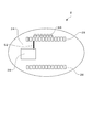
本実施形態に係る腕装着型無線通信装置9は、図12に示すように、2箇所の回路基板側端子28がダイポールアンテナ54として機能するように構成する。これにより、高性能なアンテナとなるので送信効率、受信感度が向上する。モノポールアンテナでは、その性能を発揮させるためには大面積のGNDが必要であるが、腕装着型無線通信装置のような小型装置では十分に確保することが困難である。一方、ダイポールアンテナは原理的にGNDを必要としないため腕装着型無線通信装置のような小型無線装置においては好適である。
As shown in FIG. 12, the arm-mounted
(第8の実施形態)
図13は、本実施形態に係るアンテナの構成を示す図である。尚、本実施形態の説明において、前述の実施形態と同一の構成については同一の符号を付し、その説明を省略する。
(Eighth embodiment)
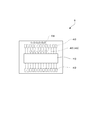
FIG. 13 is a diagram illustrating a configuration of the antenna according to the present embodiment. In the description of the present embodiment, the same components as those of the above-described embodiment are denoted by the same reference numerals, and the description thereof is omitted.
本実施形態に係る腕装着型無線通信装置9は、図13に示すように、2箇所の回路基板側端子28がダイバーシティーアンテナ56として機能するように構成する。これにより、2つの電波受信ルートで信号を入力させるようにしたため、受信状態の良い方のアンテナの機能を選択できるため、高性能なアンテナとなり送信効率、受信感度が向上する。
As shown in FIG. 13, the arm-mounted
尚、本実施形態を利用できる無線通信装置としては、上記に示す腕装着型無線通信装置以外にも、省スペースに高周波回路とアンテナ素子とを使用するページャー(携帯用小型無線機呼び出し機)、電話機、テレビ、GPS(Global Positioning System)等の衛星受信機、及び無線LAN(Local Area Network)等がある。 As a wireless communication device that can use this embodiment, in addition to the arm-mounted wireless communication device shown above, a pager (portable small wireless caller) that uses a high-frequency circuit and an antenna element in a space-saving manner, There are telephone sets, television sets, satellite receivers such as GPS (Global Positioning System), and wireless LAN (Local Area Network).
2,4,6,8,9…腕装着型無線通信装置(無線通信装置) 10…液晶表示パネル(表示部)(第1内部回路) 12…装置本体 14R,14L…腕バンド 16…尾錠 18…ケーシング 20…裏カバー 22…回路組立体 24…回路基板(第1回路基板) 26…回路駆動用電池 28…回路基板側端子(第1端子部) 32…表示パネル基板(第2回路基板) 36…高周波アナログIC(高周波回路) 38…信号処理用デジタルIC(第2内部回路) 40…表示パネル側端子(第2端子部) 42…ゼブラコネクター(導通手段) 46…インダクタンス素子(第1及び第2高周波遮断素子) 48…抵抗素子(第1及び第2高周波遮断素子) 52…配線 54…ダイポールアンテナ 56…ダイバーシティーアンテナ 64…パターン 68…結合コンデンサー(コンデンサー)。
2,4,6,8,9 ... Arm-mounted wireless communication device (wireless communication device) 10 ... Liquid crystal display panel (display unit) (first internal circuit) 12 ...
Claims (12)
前記複数の第1端子部と対向する複数の第2端子部が設置される第2回路基板と、
前記複数の第1端子部と前記複数の第2端子部とを導通する導通手段と、
前記第1回路基板上に設置され、前記複数の第1端子部のうち少なくとも1つに接続されるIC部と、
を含み、
前記複数の第1端子部の前記IC部に接続される端子を含む少なくとも2つの隣接する端子間は、コンデンサーを介して接続され、アンテナとして機能することを特徴とする無線通信装置。 A first circuit board on which a plurality of first terminal portions are installed;
A second circuit board on which a plurality of second terminal portions facing the plurality of first terminal portions are installed;
Conducting means for conducting the plurality of first terminal portions and the plurality of second terminal portions;
An IC part installed on the first circuit board and connected to at least one of the plurality of first terminal parts;
Including
A wireless communication apparatus, wherein at least two adjacent terminals including terminals connected to the IC part of the plurality of first terminal parts are connected via a capacitor and function as an antenna.
前記IC部は、高周波信号を送受信する高周波アナログICであることを特徴とする無線通信装置。 The wireless communication device according to claim 1,
The wireless communication apparatus, wherein the IC unit is a high-frequency analog IC that transmits and receives a high-frequency signal.
前記高周波信号は2.4GHzであることを特徴とする無線通信装置。 The wireless communication device according to claim 2,
The radio communication apparatus according to claim 1, wherein the high-frequency signal is 2.4 GHz.
前記導通手段の少なくとも一部は、前記アンテナとして機能することを特徴とする無線通信装置。 In the radio | wireless communication apparatus as described in any one of Claims 1-3,
At least a part of the conducting means functions as the antenna.
前記複数の第1端子部は、前記第1回路基板の上下又は左右に設置されていることを特徴とする無線通信装置。 In the radio | wireless communication apparatus as described in any one of Claims 1-4,
The plurality of first terminal portions are installed on the top and bottom or the left and right of the first circuit board.
前記第2回路基板上に配置され、前記複数の第2端子部のうち少なくとも1つに接続される第1内部回路を含むことを特徴とする無線通信装置。 In the radio | wireless communication apparatus as described in any one of Claims 1-5,
A wireless communication apparatus comprising a first internal circuit disposed on the second circuit board and connected to at least one of the plurality of second terminal portions.
前記第1内部回路は表示部であり、前記第2回路基板は表示パネル基板であることを特徴とする無線通信装置。 The wireless communication apparatus according to claim 6, wherein
The wireless communication apparatus, wherein the first internal circuit is a display unit, and the second circuit board is a display panel board.
前記アンテナとして機能する構成は、ダイポールアンテナであることを特徴とする無線通信装置。 The wireless communication device according to claim 5, wherein
The wireless communication apparatus is characterized in that the configuration that functions as the antenna is a dipole antenna.
前記アンテナとして機能する構成は、ダイバーシティーアンテナであることを特徴とする無線通信装置。 The wireless communication device according to claim 5, wherein
The radio communication apparatus according to claim 1, wherein the configuration functioning as the antenna is a diversity antenna.
前記第1回路基板上に設置され、前記複数の第1端子部のうち少なくとも1つに接続され、直流信号又は低周波信号が出力される第2内部回路を含み、
一端が前記第2端子部に接続され、他端が前記第1内部回路に接続される第1高周波遮断素子と、
一端が前記第1端子部に接続され、他端が前記第2内部回路に接続される第2高周波遮断素子と、の少なくとも一方をさらに含むことを特徴とする無線通信装置。 The wireless communication device according to claim 6 or 7 ,
A second internal circuit installed on the first circuit board, connected to at least one of the plurality of first terminal portions, and outputting a DC signal or a low-frequency signal;
A first high-frequency cutoff element having one end connected to the second terminal portion and the other end connected to the first internal circuit;
A wireless communication apparatus, further comprising at least one of a second high-frequency cutoff element having one end connected to the first terminal portion and the other end connected to the second internal circuit.
前記第1及び第2高周波遮断素子は、インダクタンス素子または抵抗素子であることを特徴とする無線通信装置。 The wireless communication device according to claim 10, wherein
The wireless communication apparatus, wherein the first and second high-frequency cutoff elements are inductance elements or resistance elements.
前記第2内部回路は、信号処理用のデジタルICであることを特徴とする無線通信装置。 The wireless communication device according to claim 10, wherein
The wireless communication device, wherein the second internal circuit is a digital IC for signal processing.
Priority Applications (4)
| Application Number | Priority Date | Filing Date | Title |
|---|---|---|---|
| JP2010255596A JP5724313B2 (en) | 2010-11-16 | 2010-11-16 | Wireless communication device |
| CN201110360125.1A CN102545942B (en) | 2010-11-16 | 2011-11-14 | Wireless communication device |
| US13/295,367 US8643555B2 (en) | 2010-11-16 | 2011-11-14 | Wireless communication device |
| US14/140,139 US9484627B2 (en) | 2010-11-16 | 2013-12-24 | Wireless communication device |
Applications Claiming Priority (1)
| Application Number | Priority Date | Filing Date | Title |
|---|---|---|---|
| JP2010255596A JP5724313B2 (en) | 2010-11-16 | 2010-11-16 | Wireless communication device |
Publications (3)
| Publication Number | Publication Date |
|---|---|
| JP2012109704A JP2012109704A (en) | 2012-06-07 |
| JP2012109704A5 JP2012109704A5 (en) | 2013-10-31 |
| JP5724313B2 true JP5724313B2 (en) | 2015-05-27 |
Family
ID=46047282
Family Applications (1)
| Application Number | Title | Priority Date | Filing Date |
|---|---|---|---|
| JP2010255596A Expired - Fee Related JP5724313B2 (en) | 2010-11-16 | 2010-11-16 | Wireless communication device |
Country Status (3)
| Country | Link |
|---|---|
| US (2) | US8643555B2 (en) |
| JP (1) | JP5724313B2 (en) |
| CN (1) | CN102545942B (en) |
Families Citing this family (6)
| Publication number | Priority date | Publication date | Assignee | Title |
|---|---|---|---|---|
| JP5724313B2 (en) * | 2010-11-16 | 2015-05-27 | セイコーエプソン株式会社 | Wireless communication device |
| JP5664329B2 (en) * | 2011-02-25 | 2015-02-04 | セイコーエプソン株式会社 | Wireless communication device |
| EP2747198A1 (en) | 2012-12-21 | 2014-06-25 | The Swatch Group Research and Development Ltd. | Antenna assembly for a time-piece |
| CN106707729B (en) * | 2017-01-11 | 2022-06-17 | 广东小天才科技有限公司 | Intelligent watch |
| DE102019119615A1 (en) * | 2019-07-19 | 2021-01-21 | Endress+Hauser SE+Co. KG | Encapsulable antenna unit |
| EP3882721A1 (en) * | 2020-03-18 | 2021-09-22 | Casio Computer Co., Ltd. | Display device and timepiece |
Family Cites Families (17)
| Publication number | Priority date | Publication date | Assignee | Title |
|---|---|---|---|---|
| US5280646A (en) * | 1988-03-23 | 1994-01-18 | Seiko Epson Corporation | Paging device with structure for removing static electricity |
| US5450091A (en) * | 1988-08-05 | 1995-09-12 | Seiko Epson Corporation | Variable size antenna device having resonance frequency compensation |
| JP2001035966A (en) * | 2000-01-01 | 2001-02-09 | Ngk Spark Plug Co Ltd | Wiring board and relay board |
| US6642895B2 (en) * | 2000-03-15 | 2003-11-04 | Asulab S.A. | Multifrequency antenna for instrument with small volume |
| JP4016261B2 (en) * | 2002-09-24 | 2007-12-05 | 三菱マテリアル株式会社 | RFID transponder and method for adjusting resonance frequency |
| JP2004118694A (en) * | 2002-09-27 | 2004-04-15 | Toshiba Corp | Method for mounting hybrid ic card |
| US7102587B2 (en) * | 2004-06-15 | 2006-09-05 | Premark Rwp Holdings, Inc. | Embedded antenna connection method and system |
| JP2007274609A (en) | 2006-03-31 | 2007-10-18 | Toshiba Corp | Portable digital assistant |
| US7830311B2 (en) * | 2007-07-18 | 2010-11-09 | Murata Manufacturing Co., Ltd. | Wireless IC device and electronic device |
| JP5151404B2 (en) * | 2007-11-07 | 2013-02-27 | 凸版印刷株式会社 | Composite IC card and manufacturing method thereof |
| JP2009141169A (en) | 2007-12-07 | 2009-06-25 | Shinko Electric Ind Co Ltd | Semiconductor device |
| JP4992774B2 (en) * | 2008-03-14 | 2012-08-08 | セイコーエプソン株式会社 | Electro-optical device and electronic apparatus |
| JP5354403B2 (en) * | 2009-03-19 | 2013-11-27 | 株式会社村田製作所 | ANTENNA DEVICE AND RADIO COMMUNICATION DEVICE |
| JP2011250233A (en) | 2010-05-28 | 2011-12-08 | Seiko Epson Corp | Radio communication device |
| JP2012039487A (en) | 2010-08-10 | 2012-02-23 | Seiko Epson Corp | Radio communication device |
| JP5724313B2 (en) * | 2010-11-16 | 2015-05-27 | セイコーエプソン株式会社 | Wireless communication device |
| JP5664329B2 (en) | 2011-02-25 | 2015-02-04 | セイコーエプソン株式会社 | Wireless communication device |
-
2010
- 2010-11-16 JP JP2010255596A patent/JP5724313B2/en not_active Expired - Fee Related
-
2011
- 2011-11-14 CN CN201110360125.1A patent/CN102545942B/en not_active Expired - Fee Related
- 2011-11-14 US US13/295,367 patent/US8643555B2/en not_active Expired - Fee Related
-
2013
- 2013-12-24 US US14/140,139 patent/US9484627B2/en active Active
Also Published As
| Publication number | Publication date |
|---|---|
| US20120119962A1 (en) | 2012-05-17 |
| US20140184458A1 (en) | 2014-07-03 |
| CN102545942B (en) | 2015-06-10 |
| CN102545942A (en) | 2012-07-04 |
| JP2012109704A (en) | 2012-06-07 |
| US8643555B2 (en) | 2014-02-04 |
| US9484627B2 (en) | 2016-11-01 |
Similar Documents
| Publication | Publication Date | Title |
|---|---|---|
| CN204481122U (en) | Electronic equipment | |
| CN203277656U (en) | Electronic device and antenna | |
| JP5724313B2 (en) | Wireless communication device | |
| KR100799719B1 (en) | Slot antenna device | |
| US7825860B2 (en) | Antenna assembly | |
| CN103427150A (en) | Antenna and proximity sensor structures having printed circuit and dielectric carrier layers | |
| US9692099B2 (en) | Antenna-matching device, antenna device and mobile communication terminal | |
| US20090091507A1 (en) | Antenna device with an isolating unit | |
| US7768463B2 (en) | Antenna assembly, printed wiring board and device | |
| US11431079B2 (en) | Antenna module including a flexible substrate | |
| CN101232119B (en) | Electronic apparatus | |
| JP2007129304A (en) | High frequency wireless module | |
| KR101153165B1 (en) | High frequency transmission line using printed circuit board | |
| US20080261667A1 (en) | Mobile terminal having an improved internal antenna | |
| US7583237B2 (en) | Antenna module having a multilayered substrate with built-in components which are connected to mounted components | |
| GB2430307A (en) | Compact balanced antenna arrangement | |
| JP2010028494A (en) | Antenna and electric appliance equipped with the same | |
| JP5664329B2 (en) | Wireless communication device | |
| US20060012526A1 (en) | Antenna with filter | |
| JP2006197528A (en) | Folded linear inverse f-shaped antenna | |
| CN113410623B (en) | Antenna device and electronic apparatus | |
| US20090052360A1 (en) | Information terminal device | |
| JP2020521403A (en) | Antenna assembly | |
| JP2012039487A (en) | Radio communication device | |
| JP2011250233A (en) | Radio communication device |
Legal Events
| Date | Code | Title | Description |
|---|---|---|---|
| A521 | Request for written amendment filed |
Free format text: JAPANESE INTERMEDIATE CODE: A523 Effective date: 20130913 |
|
| A621 | Written request for application examination |
Free format text: JAPANESE INTERMEDIATE CODE: A621 Effective date: 20130913 |
|
| A977 | Report on retrieval |
Free format text: JAPANESE INTERMEDIATE CODE: A971007 Effective date: 20140410 |
|
| A131 | Notification of reasons for refusal |
Free format text: JAPANESE INTERMEDIATE CODE: A131 Effective date: 20140430 |
|
| A521 | Request for written amendment filed |
Free format text: JAPANESE INTERMEDIATE CODE: A523 Effective date: 20140624 |
|
| A131 | Notification of reasons for refusal |
Free format text: JAPANESE INTERMEDIATE CODE: A131 Effective date: 20140924 |
|
| A521 | Request for written amendment filed |
Free format text: JAPANESE INTERMEDIATE CODE: A523 Effective date: 20141120 |
|
| RD04 | Notification of resignation of power of attorney |
Free format text: JAPANESE INTERMEDIATE CODE: A7424 Effective date: 20150106 |
|
| A131 | Notification of reasons for refusal |
Free format text: JAPANESE INTERMEDIATE CODE: A131 Effective date: 20150106 |
|
| A521 | Request for written amendment filed |
Free format text: JAPANESE INTERMEDIATE CODE: A523 Effective date: 20150213 |
|
| TRDD | Decision of grant or rejection written | ||
| A01 | Written decision to grant a patent or to grant a registration (utility model) |
Free format text: JAPANESE INTERMEDIATE CODE: A01 Effective date: 20150303 |
|
| A61 | First payment of annual fees (during grant procedure) |
Free format text: JAPANESE INTERMEDIATE CODE: A61 Effective date: 20150316 |
|
| R150 | Certificate of patent or registration of utility model |
Ref document number: 5724313 Country of ref document: JP Free format text: JAPANESE INTERMEDIATE CODE: R150 |
|
| S531 | Written request for registration of change of domicile |
Free format text: JAPANESE INTERMEDIATE CODE: R313531 |
|
| R350 | Written notification of registration of transfer |
Free format text: JAPANESE INTERMEDIATE CODE: R350 |
|
| LAPS | Cancellation because of no payment of annual fees |