EP1401046A1 - Nonreciprocal circuit element and method of manufacturing the same - Google Patents
Nonreciprocal circuit element and method of manufacturing the same Download PDFInfo
- Publication number
- EP1401046A1 EP1401046A1 EP03255741A EP03255741A EP1401046A1 EP 1401046 A1 EP1401046 A1 EP 1401046A1 EP 03255741 A EP03255741 A EP 03255741A EP 03255741 A EP03255741 A EP 03255741A EP 1401046 A1 EP1401046 A1 EP 1401046A1
- Authority
- EP
- European Patent Office
- Prior art keywords
- magnetic plate
- center conductors
- circuit element
- nonreciprocal circuit
- capacitors
- Prior art date
- Legal status (The legal status is an assumption and is not a legal conclusion. Google has not performed a legal analysis and makes no representation as to the accuracy of the status listed.)
- Granted
Links
- 238000004519 manufacturing process Methods 0.000 title claims description 22
- 239000004020 conductor Substances 0.000 claims abstract description 185
- 239000003990 capacitor Substances 0.000 claims description 94
- 229910000679 solder Inorganic materials 0.000 claims description 56
- 238000007747 plating Methods 0.000 claims description 38
- 125000006850 spacer group Chemical group 0.000 claims description 25
- 238000000034 method Methods 0.000 description 17
- 239000000470 constituent Substances 0.000 description 10
- 238000005476 soldering Methods 0.000 description 7
- 229910000859 α-Fe Inorganic materials 0.000 description 5
- BQCADISMDOOEFD-UHFFFAOYSA-N Silver Chemical compound [Ag] BQCADISMDOOEFD-UHFFFAOYSA-N 0.000 description 4
- 229910052709 silver Inorganic materials 0.000 description 4
- 239000004332 silver Substances 0.000 description 4
- 238000005245 sintering Methods 0.000 description 4
- 230000001413 cellular effect Effects 0.000 description 3
- 239000000843 powder Substances 0.000 description 3
- XEEYBQQBJWHFJM-UHFFFAOYSA-N Iron Chemical compound [Fe] XEEYBQQBJWHFJM-UHFFFAOYSA-N 0.000 description 2
- BGPVFRJUHWVFKM-UHFFFAOYSA-N N1=C2C=CC=CC2=[N+]([O-])C1(CC1)CCC21N=C1C=CC=CC1=[N+]2[O-] Chemical compound N1=C2C=CC=CC2=[N+]([O-])C1(CC1)CCC21N=C1C=CC=CC1=[N+]2[O-] BGPVFRJUHWVFKM-UHFFFAOYSA-N 0.000 description 2
- 239000004642 Polyimide Substances 0.000 description 2
- 239000011230 binding agent Substances 0.000 description 2
- 230000005540 biological transmission Effects 0.000 description 2
- 230000003247 decreasing effect Effects 0.000 description 2
- 230000002349 favourable effect Effects 0.000 description 2
- 230000002401 inhibitory effect Effects 0.000 description 2
- 229920001721 polyimide Polymers 0.000 description 2
- 229910001030 Iron–nickel alloy Inorganic materials 0.000 description 1
- 229910045601 alloy Inorganic materials 0.000 description 1
- 239000000956 alloy Substances 0.000 description 1
- 239000011248 coating agent Substances 0.000 description 1
- 238000000576 coating method Methods 0.000 description 1
- 230000004907 flux Effects 0.000 description 1
- 239000002223 garnet Substances 0.000 description 1
- 229910052742 iron Inorganic materials 0.000 description 1
- 238000010030 laminating Methods 0.000 description 1
- 238000003475 lamination Methods 0.000 description 1
- 238000010295 mobile communication Methods 0.000 description 1
- 238000012986 modification Methods 0.000 description 1
- 230000004048 modification Effects 0.000 description 1
- 230000008054 signal transmission Effects 0.000 description 1
- 239000000758 substrate Substances 0.000 description 1
Images




Classifications
-
- H—ELECTRICITY
- H01—ELECTRIC ELEMENTS
- H01P—WAVEGUIDES; RESONATORS, LINES, OR OTHER DEVICES OF THE WAVEGUIDE TYPE
- H01P1/00—Auxiliary devices
- H01P1/32—Non-reciprocal transmission devices
- H01P1/38—Circulators
- H01P1/383—Junction circulators, e.g. Y-circulators
- H01P1/387—Strip line circulators
-
- H—ELECTRICITY
- H01—ELECTRIC ELEMENTS
- H01P—WAVEGUIDES; RESONATORS, LINES, OR OTHER DEVICES OF THE WAVEGUIDE TYPE
- H01P11/00—Apparatus or processes specially adapted for manufacturing waveguides or resonators, lines, or other devices of the waveguide type
Definitions
- the present invention in yet another aspect thereof, provides a method of manufacturing a nonreciprocal circuit element according to the present invention is such that a plurality of insulating films having center conductors and capacitors is laminated on a side of a first surface of a magnetic plate having through holes, and a common electrode is formed on a side associated with a second surface of the magnetic plate, and terminal electrodes are engaged with side edges, adjacent to the first ends of the magnetic plate.
- the thickness of the capacitors 14a to 14c are substantially the same as the thickness of the crossing portion of the first, second, and third center conductors 12a to 12c, although it depends on the electrostatic capacitances. More specifically, a thickness on the order of 0.1 mm is preferable.
- solder plating layers 4a to 4e on the insulating layer 4 can be omitted by applying solder plating or cream-like solder on the first to third capacitors 14a to 14c and the terminating resistor 15 so that the associated center conductors are extended and overlapped.
- the magnetic plate 11 has a plurality of through holes 16a 1 to 16c.
- the thickness of the second capacitor 14b is substantially the same as the thickness of the insulating film 53a, although it depends on electrostatic capacitance.
- the thickness of the third capacitor 14c is substantially the same as the total thickness of the insulating films 53a and 53b.
- the first capacitor 14a is preferably as thin as possible.
- the arrangement may be such that a portion of the insulating film 53c over the capacitor 14b and the insulating films 53b and 53c over the first capacitor 14a are eliminated to absorb the thickness of the capacitors.
Landscapes
- Engineering & Computer Science (AREA)
- Manufacturing & Machinery (AREA)
- Non-Reversible Transmitting Devices (AREA)
Abstract
Description
- The present invention relates to nonreciprocal circuit elements and methods of manufacturing a nonreciprocal circuit element. Particularly, the present invention relates to a nonreciprocal circuit element that is small in size, that exhibits high performance, and that is suitable for mass production, and to a manufacturing method thereof.
- Lumped-constant isolators, which are a type of nonreciprocal circuit element, are high-frequency components that allow signals to be transmitted in a direction of transmission without a loss while inhibiting transmission of signals in the opposite direction, and are used in transmission circuits of mobile communication devices such as cellular phones. Recently, as the sizes of cellular phones become smaller, a demand exists for further miniaturization of isolators used in cellular phones.
- As nonreciprocal circuit elements that are similar to isolators, circulators are known. Techniques for reducing the sizes of circulators and improving performance thereof are disclosed in Fig. 10 of Japanese Unexamined Patent Application Publication No. 6-338707. Fig. 10 of Japanese Unexamined Patent Application Publication No. 6-338707 discloses a circulator in which conductors are embedded in a YIG lamination and the conductors are connected to a magnetic rotor via through holes or the like in order to reduce size and improve performance.
- The magnetic rotor mentioned above is manufactured by coating green sheets composed of YIG powder, binder, and flux with silver paste or the like by printing or the like, and sintering the green sheets. However, when silver paste or the like is used, sintering temperature must be kept low. This has lead to insufficient sintering and failure to obtain a YIG magnetic component having satisfactory characteristics. Thus, it has been difficult to improve performance of circulators.
- Furthermore, the magnetic rotor manufactured has a polygonal shape. Thus, when the magnetic rotor is contained in a substantially rectangular-parallelepiped case, a useless space is formed between the magnetic rotor and the case, inhibiting miniaturization of circulators.
- The present invention has been made in view of the situation described above, and an object thereof is to provide a nonreciprocal circuit element and an isolator that are small in size, that exhibit high performance, and that are suitable for mass production, and to a method of manufacturing a nonreciprocal circuit element.
- In order to achieve the above object, the present invention employs the following schemes.
- The present invention, in one aspect thereof, provides a nonreciprocal circuit element including a magnetic plate having a plurality of through holes; a plurality of center conductors crossing each other at a predetermined angle on a side associated with a first surface of the magnetic plate; and a common electrode disposed on a side associated with a second surface of the magnetic plate and connected to the center conductors via the through holes.
- According to the nonreciprocal circuit element, since a magnetic plate having through holes formed in advance is used, a magnetic plate having favorable characteristics can be used, serving to improve characteristics of the nonreciprocal circuit element.
- Preferably, in the nonreciprocal circuit element, the magnetic plate is contained in a case, and at least one of a vertical dimension and a horizontal dimension of the magnetic plate substantially coincides with a vertical dimension or a horizontal dimension of an interior of the case.
- According to the nonreciprocal circuit element, since the sizes of the case and the magnetic plate substantially coincide with each other, a large planar area can be occupied by the magnetic plate even if the case is small. Accordingly, L (inductances) can be increased and C (capacitances) can be decreased by increasing the lengths of the center conductors, serving to suppress loss caused by the nonreciprocal circuit element.
- Also preferably, in the nonreciprocal circuit element, capacitors connected to first ends of the center conductors are disposed on the side associated with the first surface of the magnetic plate.
- According to the nonreciprocal circuit element, a space for disposing the capacitors need not be provided separately from a space for disposing the magnetic plate. Accordingly, the nonreciprocal circuit element can be implemented in a small size. Furthermore, loss can be reduced by increasing a planar area occupied by the magnetic plate and improving L of the center conductors.
- Also preferably, in the nonreciprocal circuit element, the case is formed by a first yoke disposed on the side associated with the first surface of the magnetic plate, and a second yoke disposed on the side associated with the second surface of the magnetic plate so as to also function as a grounding electrode, the capacitors being connected to the second yoke via other through holes provided in the magnetic plate.
- According to the nonreciprocal circuit element, since the capacitors are connected to the grounding electrode via the through holes provided in the magnetic plate, connecting wires need not be provided. Thus, the structure of the nonreciprocal circuit element can be simplified to improve mass productivity, and the nonreciprocal circuit element can be implemented in a small size.
- Also preferably, in the nonreciprocal circuit element, terminal electrodes connected to the first ends of the center conductors are engaged with side edges of the magnetic plate.
- According to the nonreciprocal circuit element, since the terminal electrodes are engaged with the side edges of the magnetic plate, a space for disposing the terminal electrodes can be reduced, so that the nonreciprocal circuit element can be implemented in a small size.
- Also preferably, in the nonreciprocal circuit element, the center conductors are formed, by printing, over the magnetic plate via insulating layers.
- According to the nonreciprocal circuit element, since the center conductors are formed by printing, as opposed to known nonreciprocal circuit elements, the center conductors need not be bent, and the center conductors can be precisely positioned over the magnetic plate.
- Furthermore, since the center conductors can be formed thin, the nonreciprocal circuit element can be implemented in a small size.
- Also preferably, in the nonreciprocal circuit element, an insulating spacer and a biasing permanent magnet are laminated on the side of the first surface of the magnetic plate, solder plating layers are formed on one surface, associated with the magnetic plate, of the insulating spacer, the solder plating layers electrically connecting the first ends of the center conductors to the capacitors and the terminal electrodes, respectively.
- According to the nonreciprocal circuit element, since the center conductors are connected to the capacitors and the terminal electrodes via the solder plating layers, connecting wires need not be provided. Thus, the structure of the nonreciprocal circuit element can be simplified to improve mass productivity, and the nonreciprocal circuit element can be implemented in a small size. Furthermore, by forming the solder plating layers thin, the nonreciprocal circuit element can be implemented in an even smaller size.
- Also preferably, in the nonreciprocal circuit element, the center conductors are formed on insulating films, and the insulating films are laminated over the magnetic plate with the center conductors facing the magnetic plate.
- According to the nonreciprocal circuit element, since the insulating film having the center conductors are laminated, as opposed to known nonreciprocal circuit elements, the center conductors need not be bent, and the center conductors can be precisely positioned on the magnetic plate.
- Furthermore, since the center conductors can be formed thin, the nonreciprocal circuit element can be implemented in a small size.
- Also preferably, in the nonreciprocal circuit element, the capacitors are disposed on the insulating films.
- According to the nonreciprocal circuit element, since the center conductors can be connected to the capacitors within the insulating films, connecting wires need not be newly provided. Thus, the structure of the nonreciprocal circuit element can be simplified to improve mass productivity, and the nonreciprocal circuit element can be implemented in a small size.
- Furthermore, in the nonreciprocal circuit element, a terminating resistor may be connected to one of the center conductors of the nonreciprocal circuit element according to one of the arrangements described above.
- According to the nonreciprocal circuit element, the nonreciprocal circuit element is small in size and is suitable for mass production.
- Preferably, in the nonreciprocal circuit element, the terminating resistor is mounted on the second yoke, and the terminating resistor is electrically connected to the center conductors via another solder plating layer formed on one surface, associated with the magnetic plate, of the insulating spacer.
- According to the nonreciprocal circuit element, since the terminating resistor is mounted on the second yoke, a connecting wire can be omitted. Furthermore, since the terminating resistor is connected to the center conductor via the solder plating layer, a connecting wire need not be provided. Thus, the structure of the nonreciprocal circuit element can be simplified to improve mass productivity, and the nonreciprocal circuit element can be implemented in a small size.
- The present invention, in another aspect thereof, provides a method of manufacturing a nonreciprocal circuit element according to the present invention is such that a plurality of center conductors is laminated, via insulating layers, on a side associated with a first surface of a magnetic plate having through holes, and a common electrode is formed on a side associated with a second surface of the magnetic plate, capacitors are disposed in proximity to first ends of the center conductors, and terminal electrodes are engaged with side edges, adjacent to the first ends, of the magnetic plate, an insulating spacer having solder plating layers is laminated over the magnetic plate such that the solder plating layers are opposed at least to the first ends of the center conductors, and the solder plating layers are melted by heat to electrically connect the first ends to the capacitors and the terminal electrodes, respectively.
- According to the method of manufacturing a nonreciprocal circuit element, an insulating spacer is laminated on center conductors, and solder plating layers are melted by heat to electrically connect the center conductors to terminal electrodes, respectively. Accordingly, a process of bending center conductors and a process of individually soldering capacitors and terminal electrodes, which have hitherto been required, are omitted, serving to improve productivity.
- Furthermore, since the method simply incorporates constituent components sequentially and applies heat thereto, the constituent components can be precisely positioned and assembled.
- The present invention, in yet another aspect thereof, provides a method of manufacturing a nonreciprocal circuit element according to the present invention is such that a plurality of insulating films having center conductors and capacitors is laminated on a side of a first surface of a magnetic plate having through holes, and a common electrode is formed on a side associated with a second surface of the magnetic plate, and terminal electrodes are engaged with side edges, adjacent to the first ends of the magnetic plate.
- According to the method of manufacturing a nonreciprocal circuit element, the method simply mounts center conductors and capacitors simultaneously on a magnetic plate and incorporates a common electrode and terminal electrodes. Thus, a process of bending center conductors and encapsulating YIG ferrite and a process of individually soldering capacitors and terminal electrodes, which have hitherto been required, are omitted, serving to improve productivity. Furthermore, since the method simply incorporates constituent components sequentially, the constituent components can be precisely positioned and assembled.
- Preferably, in the method of manufacturing a nonreciprocal circuit element according to the present invention, preferably, the center conductors are connected to the common electrode via the through holes.
- Embodiments of the invention will now be described, by way of example only, with reference to the accompanying drawings, in which:
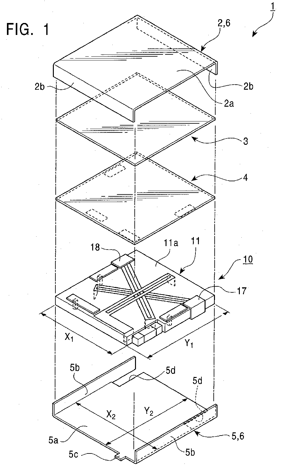
- Fig. 1 is an exploded perspective view of an isolator according to a first embodiment of the present invention;
- Fig. 2 is an exploded perspective view of main parts of the isolator according to the first embodiment of the present invention;
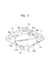
- Fig. 3 is an exploded perspective view of the main parts of the isolator according to the first embodiment of the present invention;
- Figs. 4A to 4C are process charts for explaining a method of manufacturing the isolator according to the first embodiment;
- Figs. 5A and 5B are process charts for explaining the method of manufacturing the isolator according to the first embodiment; and
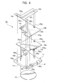
- Fig. 6 is an exploded perspective view of main parts of an isolator according to a second embodiment of the present invention.
-
- Now, a first embodiment of the present invention will be described with reference to the drawings.
- Fig. 1 shows an exploded perspective view of an isolator as an example of a nonreciprocal circuit element according to the first embodiment of the present invention. Fig. 2 shows a perspective view of main parts of the isolator. Fig. 3 shows a perspective view of the main parts of the isolator as viewed from another direction.
- As shown in Fig. 1, an
isolator 1 according to this embodiment includes, as main components, a first yoke 2 (case 6), a biasingpermanent magnet 3, an insulatingspacer 4, a magnetic-component assembly 10, and a second yoke 5 (case 6). - The
permanent magnet 3 applies a DC bias magnetic field to amagnetic plate 11 included in the magnetic-component assembly 10. The insulatingspacer 4 is disposed between thepermanent magnet 3 and the magnetic-component assembly 10 to prevent contact therebetween. - The
first yoke 2 and thesecond yoke 5 are engaged with each other to form a case 6 of theisolator 1. Furthermore, thesecond yoke 5 also functions as a grounding electrode of theisolator 1. These yokes are implemented by soft magnetic plates such as soft iron plates or NiFe alloy plates. With regard to thefirst yoke 2, a soft magnetic plate is bent in a horseshoe shape to form anupper plate 2a andwalls second yoke 5, abottom plate 5a andwalls bottom plate 5a has a protrudinggrounding terminal 5c that serves as a terminal of the grounding electrode. Furthermore, thebottom plate 5a hascutaway portions terminal electrodes component assembly 10. - The
first yoke 2 and thesecond yoke 5 are engaged with each other to form the case 6 having the shape of a hollow rectangular parallelepiped, and thepermanent magnet 3, the insulatingspacer 4, and the magnetic-component assembly 10 are contained inside the case 6. - As shown in Figs. 1 to 3, the magnetic-
component assembly 10 includes themagnetic plate 11, first, second, andthird center conductors 12a to 12c disposed on a side associated with afirst surface 11a of themagnetic plate 11, first, second, andthird capacitors 14a to 14c disposed on the side associated with thefirst surface 11a of themagnetic plate 11, and a terminatingresistor 15.
Furthermore, as shown in Fig. 3, acommon electrode 13 is disposed on a side associated with asecond surface 11b of themagnetic plate 11. - The
magnetic plate 11 is formed by sintering ferrite powder such as YIG ferrite (Yttrium-iron-garnet ferrite) powder together with binder or the like at a temperature of 1400°C to 1500°C, and themagnetic plate 11 has acutaway portion 11c at a part thereof. - Furthermore, the
magnetic plate 11 has a plurality of through holes 16a1 to 16c running therethrough from thefirst surface 11a to thesecond surface 11b. More specifically, themagnetic plate 11 has through holes 16a1 to 16a3 electrically connecting thecenter conductors 12a to 12c to thecommon electrode 13, and through holes 16b1 to 16b3 electrically connecting thecapacitors 14a to 14c to thebottom surface 5a (grounding electrode) of thesecond yoke 5. Furthermore, themagnetic plate 11 has another throughhole 16c electrically connecting afirst end 12c1 of the third center conductor 12 to thebottom surface 5a. - Each of the through holes 16a1 to 16c is filled with a conductive material such as silver paste to form electrical connections between the
center conductors 12a to 12c and thecommon electrode 13, between thecapacitors 14a to 14c and thebottom surface 5a, etc. - Since the sintered
magnetic plate 11 with the through holes 16a1 to 16c formed in advance is used, themagnetic plate 11 that can be sufficiently sintered and that have favorable characteristics can be used, serving to improve characteristics of theisolator 1. - Furthermore, as shown in Fig. 1, the
magnetic plate 11 is contained in the case 6 as a component of the magnetic-component assembly 10. Let the vertical dimension of themagnetic plate 11 be denoted as Y1 and the horizontal dimension thereof as X1, and let the vertical dimension of the bottom plate of the second yoke 5 (case 6) be denoted as Y2 and the horizontal dimension thereof as X2, as shown in Fig. 1. Then, the sizes of themagnetic plate 11 and the case 6 are chosen so that Y1 and Y2 substantially coincide with X1 and X2, respectively. - Thus, the size of the magnetic-
component assembly 10 as viewed in plan substantially coincides with the size of thebottom plate 5a of thesecond yoke 5 as viewed in plan. Therefore, even if the case 6 is small, a large planar area can be occupied by themagnetic plate 11. Accordingly, L (inductance) can be improved by increasing the lengths of thecenter conductors 12a to 12c. - The
center conductors 12a to 12c include afirst center conductor 12a that is laminated by printing above thefirst surface 11a of themagnetic plate 11 via an insulating layer not shown, asecond center conductor 12b that is laminated by printing above thefirst center conductor 12a at an angle of approximately 120° via an insulating layer formed by printing or the like, and athird center conductor 12c that is laminated by printing above thesecond center conductor 12b at an angle of approximately 120° via an insulating layer. As mentioned above, thecenter conductors 12a to 12c cross each other at a predetermined angle. The total thickness of the crossing portion is on the order of 0.1 µm. Thus, between themagnetic plate 11 and the insulatingspacer 4, a gap corresponding to the thickness of the crossing portion of thecenter conductors 12a to 12c is formed. - Since the
center conductors 12a to 12c are formed by printing; as opposed to known nonreciprocal circuit elements, center conductors need not be bent, and YIG ferrite need not be encapsulated. Accordingly, thecenter conductors 12a to 12c can be precisely positioned on themagnetic plate 11. Furthermore, since thecenter conductors 12a to 12c can be formed thin, theisolator 1 can be implemented in a small size. - As shown in Figs. 2 and 3, the
first center conductor 12a is disposed with afirst end 12a1 thereof in proximity to theterminal electrode 17 for input and asecond end 12a2 thereof overlapping the through hole 16a1. Thesecond end 12a2 is joined with the conductive material in the through hole 16a1 by solder or the like, whereby thefirst center conductor 12a is connected to thecommon electrode 13. - Similarly, the
second center conductor 12b is disposed with afirst end 12b1 thereof in proximity to theterminal electrode 18 for output and asecond end 12b2 thereof overlapping the through hole 16a2. The second end 12b2 is joined with the conductive material in the through hole 16a2 by solder or the like, whereby thesecond center conductor 12b is connected to thecommon electrode 13. - Furthermore, the
third center conductor 12c is disposed with afirst end 12c1 thereof in proximity to thecutaway portion 11c of themagnetic plate 11 and asecond end 12c2 thereof overlapping the through hole 16a3. Thesecond end 12c2 is joined with the conductive material in the through hole 16a3 by solder or the like, whereby thethird center conductor 12c is connected to thecommon electrode 13. - Furthermore, the
first end 12c1 of the third center conductor also overlaps the throughhole 16c. Thefirst end 12c1 is joined with the conductive material in the throughhole 16c by solder or the like, whereby thethird center conductor 12c is connected to thebottom plate 5a (grounding electrode). - As shown in Fig. 3, the
common electrode 13 is laminated over thesecond surface 11b of themagnetic plate 11 via an insulating layer not shown. Thecommon electrode 13 is formed so as to overlap the through holes 16a1 to 16a3, and is connected to thecenter conductors 12a to 12c via the through holes 16a1 to 16a3, respectively. However, thecommon electrode 13 is not needed if thecenter conductors 12a to 12c are directly connected to thebottom plate 5a (grounding electrode) of thesecond yoke 5 via the through holes 16a1 to 16a3, respectively. - Thus, the
center conductors 12a to 12c and thecommon electrode 13 are disposed so as to sandwich themagnetic plate 11, thereby forming a microstrip line. - The
capacitors 14a to 14c are disposed on the side associated with thefirst surface 11a of themagnetic plate 11, and include afirst capacitor 14a disposed in proximity to thefirst end 12a1 of the first center conductor, asecond capacitor 14b disposed in proximity to thefirst end 12b1 of the second center conductor, and athird capacitor 14c disposed in proximity to thefirst end 12c1 of the third center conductor. Thecapacitors 14a to 14c are so-called parallel-plate capacitors, and have C (electrostatic capacitances) in accordance with L (inductances) of thecenter conductors 12a to 12c, respectively. - Preferably, the thickness of the
capacitors 14a to 14c are substantially the same as the thickness of the crossing portion of the first, second, andthird center conductors 12a to 12c, although it depends on the electrostatic capacitances. More specifically, a thickness on the order of 0.1 mm is preferable. - Since the
capacitors 14a to 14c are disposed on the side associated with thefirst surface 11a of themagnetic plate 11 and have substantially the same thickness as the crossing portion of thecenter conductors 12a to 12c, the height of the crossing portion and the height of upper surfaces of thecapacitors 14a to 14c coincide with each other. Thus, thecapacitors 14a to 14c can be disposed in the gap between themagnetic plate 11 and the insulatingspacer 4, so that an extra space for disposing thecapacitors 14a to 14c need not be provided separately from the space for disposing themagnetic plate 11. Accordingly, theisolator 1 can be implemented in a small size. - The
first capacitor 14a is disposed so as to overlap the through hole 16b1, and a terminal of thefirst capacitor 14a is joined with the conductive material in the through hole 16b1 by solder or the like, whereby thefirst capacitor 14a is connected to thebottom plate 5a (grounding electrode) of thesecond yoke 5 via the through hole 16b1. - Similarly, the
second capacitor 14b is disposed so as to overlap the through hole 16b2, and a terminal of thesecond capacitor 14b is joined with the conductive material in the through hole 16b2 by solder or the like, whereby thesecond capacitor 14b is connected to thebottom plate 5a (grounding electrode) via the through hole 16b2. - Furthermore, the
third capacitor 14c is disposed so as to overlap the through hole 16b3, and a terminal of thethird capacitor 14c is joined with the conductive material in the through hole 16b3 by solder or the like, whereby thethird capacitor 14c is connected to thebottom plate 5a (grounding electrode) via the through hole 16b3. Furthermore, thethird capacitor 14c is disposed adjacent to thefirst end 12c1 of the third center conductor, and is electrically connected to thethird center conductor 12c via asolder plating layer 4e, which will be described later. - The through holes 16b1 to 16b3 are connected to the
bottom plate 5a on the side associated with thesecond surface 11b of the magnetic plate by solder or the like. - Since the
capacitors 14a to 14c are connected to thegrounding electrode 5a via the through holes 16b1 to 16b3, respectively, connecting wires need not be provided separately. Accordingly, the structure of theisolator 1 can be simplified to improve mass productivity, and theisolator 1 can be implemented in a small size. - Furthermore, the first, second, and
third capacitors spacer 4. - More specifically, as shown in Fig. 2,
solder plating layers surface 4a, associated with the magnetic plate, of the insulatingspacer 4. Thesolder plating layer 4b is disposed at a position opposing thefirst end 12a1 of the first center conductor and thefirst capacitor 14a. Thesolder plating layer 4c is formed at a position opposing thefirst end 12b1 of the second center conductor and thesecond capacitor 14b. Thesolder plating layer 4e is formed at a position opposing thefirst end 12c1 of the third center conductor and thethird capacitor 14c. - When the magnetic-
component assembly 10 is laminated with the insulatingspacer 4, thesolder plating layer 4b overlaps and bridges thefirst end 12a1 of the first center conductor and thefirst capacitor 14a, and thesolder plating layer 4c overlaps and bridges thefirst end 12b1 of the second center conductor and thesecond capacitor 14b. Similarly, thesolder plating layer 4e overlaps and bridges thefirst end 12c1 of the third center conductor and thethird capacitor 14c. Thus, thecapacitors - The terminating
resistor 15 is disposed outside thecutaway portion 11c of themagnetic plate 11. The terminatingresistor 15 is mounted on thebottom surface 5a (grounding electrode) of thesecond yoke 5. - The terminating
electrode 15 is connected to thefirst end 12c1 of the third center conductor via a solder plating layer, a solder-plated conductor layer, or the like disposed in the insulatingspacer 4. - More specifically, as shown in Fig. 2, a
solder plating layer 4d is formed on thesurface 4a, associated with the magnetic plate, of the insulatingspacer 4. Thesolder plating layer 4d is formed at a position opposing thefirst end 12c1 of the third center conductor and the terminatingresistor 15. When the magnetic-component assembly 10 is laminated with the insulatingspacer 4, thesolder plating layer 4d overlaps and bridges thefirst end 12c1 of the third center conductor and the terminatingresistor 15, whereby an electrical connection is formed therebetween. A terminal of the terminatingresistor 15, connected with thefirst end 12c1 of the third center conductor, and thesecond yoke 5 are mounted via an insulating film formed by printing or the like. - Since the terminating
resistor 15 is mounted on thesecond yoke 5, a connecting wire can be omitted. Furthermore, since the terminatingresistor 15 is connected to thecenter conductor 12c via thesolder plating layer 4d, a connecting wire need not be separately provided. Thus, the structure of theisolator 1 can be simplified to improve mass productivity, and theisolator 1 can be implemented in a small size. - The
terminal electrode 17 serving for input is mounted on aside edge 11d of the magnetic plate. Theterminal electrode 17 serving for input is disposed in proximity to thefirst end 12a1 of the first center conductor on theside edge 11d. - The
terminal electrode 18 serving for output is mounted on anotherside edge 11e of the magnetic plate. Theterminal electrode 17 serving for output is disposed in proximity to thefirst end 12b1 of the second conductor on theside edge 11e. - The
terminal electrodes first surface 11a to thesecond surface 11b of the magnetic plate. Since theterminal electrodes magnetic plate 11 as described above, only small spaces are occupied by theterminal electrodes isolator 1 can be implemented in a small size. - Furthermore, the solder plating layers 4a to 4e on the insulating
layer 4 can be omitted by applying solder plating or cream-like solder on the first tothird capacitors 14a to 14c and the terminatingresistor 15 so that the associated center conductors are extended and overlapped. - The
terminal electrodes terminal electrodes terminal electrodes magnetic plate 11. Alternatively, similarly to the case of thecapacitors 14a to 14c, the solder plating layers 4b and 4c are disposed so as to overlap and bridge the first ends 12a1 and 12b1 and theterminal electrodes - By connecting the
center conductors terminal electrodes isolator 1 can be simplified to improve mass productivity, and theisolator 1 can be implemented in a small size. - As described above, the
capacitors 14a to 14c for matching are connected to the first ends 12a1 to 12c1 of the respective center conductors, and the terminatingresistor 15 is connected to thefirst end 12c1 of the third center conductor. These elements are contained in the case 6 (the first andsecond yokes 2 and 5) together with thepermanent magnet 4 so that thepermanent magnet 4 is allowed to apply a DC magnetic field on the magnetic-component assembly 10, whereby theisolator 1 is formed. In theisolator 1, thefirst center conductor 12a connected to theterminal electrode 17 serves for input and thesecond center conductor 12b connected to theterminal electrode 18 serves for output. - According to the
isolator 1 described above, the sizes of the case 6 and themagnetic plate 11 substantially coincide with each other, so that a large planar area can be occupied by themagnetic plate 11. Accordingly, L (inductance) can be increased and C (capacitances of capacitors) can be decreased by extending the lengths of thecenter conductors 12a to 12c, serving to reduce loss caused by thenonreciprocal circuit element 1. - In order to manufacture the
isolator 1 described above, as shown in Fig. 4A, themagnetic plate 11 with the through holes 16a1 to 16c formed in advance is prepared, and the through holes 16a1 to 16c are filled with silver paste or the like. Then, as shown in Fig. 4B, the first, second, andthird center conductors 12a to 12c are formed by printing on the side associated with thefirst surface 11a of the magnetic plate. Between thecenter conductors 12a to 12c, and between thefirst center conductor 12a and themagnetic plate 11, insulating layers not shown are formed by means of printing or the like. Furthermore, thecenter conductors 12a to 12c are connected to the through holes 16a1 to 16a3 and 16c by soldering or the like. - Then, as shown in Fig. 4C, the
common electrode 13 is formed on the side associated with thesecond surface 11b of the magnetic plate. Thecommon electrode 13 is formed so as to overlap the through holes 16a1 to 16a3, and thecommon electrode 13 is connected to the through holes 16a1 to 16a3 by soldering or the like. However, thecommon electrode 13 is not needed if thecenter conductors 12a to 12c are directly connected to thebottom plate 5a (grounding electrode) of thesecond yoke 5 via the through holes 16a1 to 16a3. - Then, as shown in Fig. 5A, the first to
third capacitors 14a to 14c are disposed over the through holes 16b1 to 16b3 on thefirst surface 11a of the magnetic plate, and thecapacitors 14a to 14c are connected to the through holes 16b1 to 16b3 by soldering or the like. Furthermore, theterminal electrodes magnetic plate 11. - Then, as shown in Fig. 5B, the insulating
spacer 4 and thepermanent magnet 3 are sequentially laminated on the side associated with thefirst surface 11a of themagnetic plate 11, and these elements are sandwiched by the first andsecond yokes second yokes isolator 1. Furthermore, at this time, theterminal electrodes terminal holes second yoke 5. - Before combining the components, the solder plating layers 4b to 4e are formed in advance on the
surface 4a of the insulating spacer. The solder plating layers 4b to 4e are formed so as to overlap, at least, the first ends 12a1 to 12c1 of the respective center conductors. Furthermore, the terminatingresistor 15 is mounted in advance on thesecond yoke 5 such that a hot-side terminal is insulated from thesecond yoke 5 by a printed insulating film or the like. - Finally, the entire assembly is heated to melt the solder plating layers, whereby electrical connections are formed between the
center conductors 12a to 12c and thecapacitors 14a to 14c and between theterminal electrodes resistor 15. - According to the method of manufacturing the
isolator 1, described above, the insulatingspacer 4 is laminated over thecenter conductors 12a to 12c, and then the solder plating layers 4b to 4d are melted by heat to form electrical connections between thecenter conductors 12a to 12c and thecapacitors 14a to 14c and between theterminal electrodes resistor 15. Thus, a process of bending center conductors and a process of individually soldering capacitors and terminal electrodes, which have hitherto been required, are omitted, serving to improve productivity. - Furthermore, since the method simply incorporates the constituent components sequentially and then applies heat thereto, the constituent components can be precisely positioned and assembled.
- Next, an isolator according to a second embodiment of the present invention will be described with reference to the drawings.
- Fig. 6 shows an exploded perspective view of a magnetic-
component assembly 50 constituting the isolator according to the second embodiment of the present invention. - Of components constituting the magnetic-
component assembly 50 shown in Fig. 6, constituent components corresponding to the constituent components of the magnetic-component assembly 10 shown in Figs. 1 to 6 are designated by the same numerals, and descriptions thereof will be omitted or simplified. - As shown in Fig. 6, the magnetic-
component assembly 50 of the isolator according to this embodiment includes amagnetic plate 11, a plurality ofcenter conductors 52a to 52c disposed on a side associated with afirst surface 11a of themagnetic plate 11, a plurality ofcapacitors 14a to 14c disposed on the side associated with thefirst surface 11a of the magnetic plate, and a terminatingresistor 15. Furthermore, acommon electrode 13 is disposed on a side associated with asecond surface 11b of themagnetic plate 11. - Furthermore, the
magnetic plate 11 has a plurality of through holes 16a1 to 16c. - The
center conductors 52a to 52c are formed respectively on surfaces of insulatingfilms - More specifically, a
first center conductor 52a is formed on a lower surface of the insulatingfilm 53a as viewed in the figure. The insulatingfilm 53a is implemented by a flexible substrate composed of polyimide or the like. Furthermore, the insulatingfilm 53a has connectingholes third center conductors conductor 52a3 is formed at afirst end 52a1 of the first center conductor, and afirst capacitor 14a is attached from the lower surface of the insulatingfilm 53a so as to overlap the connectingconductor 52a3. - Similarly, a
second center conductor 52b is formed on a lower surface of the insulatingfilm 53b as viewed in the figure. The insulatingfilm 53b has a connectinghole 53b1 for connecting thethird center conductor 52c to the through hole 16a3. Furthermore, a connectingconductor 52b3 is formed at afirst end 52b1 of the second center conductor, and asecond capacitor 14b is attached from the lower surface of the insulatingfilm 53b so as to overlap the connectingconductor 52b3. - Furthermore, a
third center conductor 52c is formed on a lower surface of the insulatingfilm 53c as viewed in the figure. A connectingconductor 52c3 is formed at afirst end 52c1 of the third center conductor, and athird capacitor 14c is attached from the lower surface of the insulatingfilm 53c so as to overlap the connectingconductor 52c3. - The insulating
film 53a is formed in a shape such that it does not interfere with the first ends 52b1 and 52c1 of the second and third center conductors and with the second andthird capacitors film 53b is formed in a shape such that it does not interfere with thefirst end 52c1 of the third center conductor and with thethird capacitor 14c. - Thus, when the insulating
films 53a to 53c are laminated over themagnetic plate 11, the first ends 52b1 and 52c1 of the second and third center conductors and the second andthird capacitors first surface 11a of the magnetic plate without being interfered with by the insulatingfilms - More specifically, when the insulating
films 53a to 53c are laminated over themagnetic plate 11, thefirst end 52a1 of thefirst center conductor 52a overlaps theterminal electrode 17 serving for input, and these elements are connected to each other by solder or the like. Furthermore, asecond end 52a2 overlaps the through hole 16a1, and thesecond end 52a2 is joined with a conductive material in the through hole 16a1 by solder or the like, whereby thefirst center conductor 52a is connected to thecommon electrode 13. - Similarly, the
first end 52b1 of the second center conductor overlaps theterminal electrode 18 serving for output, and these elements are connected to each other by solder or the like. Furthermore, asecond end 52b2 overlaps the through hole 16a2, and thesecond end 52b2 is joined with a conductive material in the through hole 16a2 by solder or the like, whereby thesecond center conductor 52b is connected to thecommon electrode 13. - Furthermore, the
first end 53c1 of the third center conductor overlaps acutaway portion 11c of themagnetic plate 11, and asecond end 52c2 overlaps the through hole 16a3. Then, thesecond end 52c2 is joined with a conductive material in the through hole 16a3 by solder or the like, whereby thethird center conductor 52c is connected to thecommon electrode 13. - Furthermore, the
first end 53c1 of the third center conductor overlaps the throughhole 16c, and thefirst end 52c1 is joined with a conductive material in the throughhole 16c by solder or the like, whereby thethird center conductor 52c is connected to a second yoke (grounding electrode) not shown. - The
center conductors 52a to 52c and thecommon electrode 13 are disposed so as to sandwich themagnetic plate 11, whereby a microstrip line is formed. Alternatively, thecenter conductors 52a to 52c may be directly connected to the second yoke not shown via the through holes 16a1 to 16a3, respectively, in which case thecommon electrode 13 is not needed. - Furthermore, by laminating the insulating
films 53a to 53c over themagnetic plate 11, thecenter conductors 52a to 52c cross each other at a predetermined angle. - Furthermore, when the insulating
films 53a to 53c are laminated over themagnetic plate 11, thefirst capacitor 14a overlaps the through hole 16b1, and thefirst capacitor 14a is joined with a conductive material in the through hole 16b1 by solder or the like, whereby thefirst capacitor 14a is connected to the second yoke (grounding electrode) not shown. - Similarly, the
second capacitor 14b overlaps the through hole 16b2, and thesecond capacitor 14b is joined with a conductive material in the through hole 16b2 by solder or the like, whereby thesecond capacitor 14b is connected to the second yoke (grounding electrode) not shown. - Furthermore, the
third capacitor 14c overlaps the through hole 16b3, and thethird capacitor 14c is joined with a conductive material in the through hole 16b3 by solder or the like, whereby thethird capacitor 14c is connected to the second yoke (grounding electrode) not shown. - Furthermore, the
first end 53c1 of the third center conductor overlaps the terminatingresistor 15, whereby thethird center conductor 53c is connected to the terminating resistor. - Preferably, the thickness of the
second capacitor 14b is substantially the same as the thickness of the insulatingfilm 53a, although it depends on electrostatic capacitance. Also preferably, the thickness of thethird capacitor 14c is substantially the same as the total thickness of the insulatingfilms first capacitor 14a is preferably as thin as possible. Alternatively, the arrangement may be such that a portion of the insulatingfilm 53c over thecapacitor 14b and the insulatingfilms first capacitor 14a are eliminated to absorb the thickness of the capacitors. - Since the
capacitors film 53a and thecapacitor 14c does not interfere with the insulatingfilm 53b, by choosing the thickness of the second andthird capacitors capacitors magnetic plate 11 and an insulating spacer not shown, so that a space for disposing thecapacitors 14a to 14c need not be provided separately from a space for disposing themagnetic plate 11. Accordingly, theisolator 1 can be implemented in a small size. - As described above, the
capacitors 14a to 14c for matching are connected to the first ends 52a1 to 52c1 of the center conductors, respectively, and thefirst end 52c1 of the third center conductor is connected to the terminatingresistor 15. These components, together with a permanent magnet not shown, are contained in a case (first and second yokes) not shown so that a DC magnetic field can be applied to the magnetic-component assembly 50, whereby the isolator according to this embodiment is formed. In this isolator, thefirst center conductor 52a connected to theterminal electrode 17 serves for input, and thesecond center conductor 52b connected to theterminal electrode 18 serves for output. - According to the isolator of this embodiment, the
center conductors 52a to 52c are formed on the insulatingfilms 53a to 53c, respectively, and the insulatingfilms 53a to 53c are laminated over themagnetic plate 11. Thus, as opposed to known nonreciprocal circuit elements, center conductors need not be bent, and thecenter conductors 53a to 53c can be precisely positioned with respect to themagnetic plate 11. Furthermore, thecenter conductors 52a to 52c can be formed thin, so that the isolator can be implemented in a small size. - In order to manufacture the isolator according to this embodiment, the insulating
films 53a to 53c with thecenter conductors 53a to 53c and thecapacitors 14a to 14c formed in advance are sequentially laminated on the side associated with thefirst surface 11a of the magnetic plate, thecommon electrode 13 is formed on the side associated with thesecond surface 11b of the magnetic plate, and theterminal electrodes side edges magnetic plate 11, whereby the magnetic-component assembly 50 shown in Fig. 6 is formed. The magnetic-component assembly 50, together with the insulating spacer and the permanent magnet, is contained in the case formed by the first and second yokes, and theterminal electrodes - This manufacturing method simply mounts the
center conductors 52a to 52c and thecapacitors 14a to 14c simultaneously on themagnetic plate 11 and incorporates thecommon electrode 13 and theterminal electrodes - The technical scope of the present invention is not limited to the embodiments described above, and various modifications can be made without departing from the spirit of the present invention. For example, although the first and second embodiments described above relate to isolators in which a terminating resistor is connected to a third center conductor, a terminal electrode may be connected to the third center conductor to form a circulator.
Claims (15)
- A nonreciprocal circuit element comprising a magnetic plate having a plurality of through holes; a plurality of center conductors crossing each other at a predetermined angle on a side associated with a first surface of the magnetic plate; and a common electrode disposed on a side associated with a second surface of the magnetic plate and connected to the center conductors via the through holes.
- A nonreciprocal circuit element according to Claim 1, wherein the magnetic plate is contained in a case, and at least one of a vertical dimension and a horizontal dimension of the magnetic plate substantially coincides with a vertical dimension or a horizontal dimension of an interior of the case.
- A nonreciprocal circuit element according to Claim 1, wherein capacitors connected to first ends of the center conductors are disposed on the side associated with the first surface of the magnetic plate.
- A nonreciprocal circuit element according to Claim 3, wherein the case is formed by a first yoke disposed on the side associated with the first surface of the magnetic plate, and a second yoke disposed on the side associated with the second surface of the magnetic plate so as to also function as a grounding electrode, the capacitors being connected to the second yoke via other through holes provided in the magnetic plate.
- A nonreciprocal circuit element according to Claim 1, wherein terminal electrodes connected to the first ends of the center conductors are engaged with side edges of the magnetic plate.
- A nonreciprocal circuit element according to Claim 1, wherein the center conductors are formed, by printing, over the magnetic plate via insulating layers.
- A nonreciprocal circuit element according to Claim 3, wherein an insulating spacer and a biasing permanent magnet are laminated on the side of the first surface of the magnetic plate, solder plating layers are formed on one surface, associated with the magnetic plate, of the insulating spacer, the solder plating layers electrically connecting the first ends of the center conductors to the capacitors and the terminal electrodes, respectively.
- A nonreciprocal circuit element according to Claim 1, wherein the center conductors are formed on insulating films, and the insulating films are laminated over the magnetic plate with the center conductors facing the magnetic plate.
- A nonreciprocal circuit element according to Claim 8, wherein the capacitors are disposed on the insulating films.
- A nonreciprocal circuit element according to Claim 1, wherein a terminating resistor is connected to one of the center conductors.
- A nonreciprocal circuit element according to Claim 10, wherein the terminating resistor is mounted on the second yoke, and the terminating resistor is electrically connected to the center conductors via another solder plating layer formed on one surface, associated with the magnetic plate, of the insulating spacer.
- A method of manufacturing a nonreciprocal circuit element,
wherein a plurality of center conductors is laminated, via insulating layers, on a side associated with a first surface of a magnetic plate having through holes, and a common electrode is formed on a side associated with a second surface of the magnetic plate,
capacitors are disposed in proximity to first ends of the center conductors, and terminal electrodes are engaged with side edges, adjacent to the first ends, of the magnetic plate,
an insulating spacer having solder plating layers is laminated over the magnetic plate such that the solder plating layers are opposed at least to the first ends of the center conductors,
and the solder plating layers are melted by heat to electrically connect the first ends to the capacitors and the terminal electrodes, respectively. - A method of manufacturing a nonreciprocal circuit element,
wherein a plurality of insulating films having center conductors and capacitors is laminated on a side of a first surface of a magnetic plate having through holes, and a common electrode is formed on a side associated with a second surface of the magnetic plate,
and terminal electrodes are engaged with side edges, adjacent to first ends of the center conductors, of the magnetic plate. - A method of manufacturing a nonreciprocal circuit element according to Claim 12, wherein the center conductors are connected to the common electrode via the through holes.
- A method of manufacturing a nonreciprocal circuit element according to Claim 13, wherein the center conductors are connected to the common electrode via the through holes.
Applications Claiming Priority (2)
| Application Number | Priority Date | Filing Date | Title |
|---|---|---|---|
| JP2002275582A JP3939622B2 (en) | 2002-09-20 | 2002-09-20 | Non-reciprocal circuit element, isolator, and non-reciprocal circuit element manufacturing method |
| JP2002275582 | 2002-09-20 |
Publications (2)
| Publication Number | Publication Date |
|---|---|
| EP1401046A1 true EP1401046A1 (en) | 2004-03-24 |
| EP1401046B1 EP1401046B1 (en) | 2006-05-17 |
Family
ID=31944613
Family Applications (1)
| Application Number | Title | Priority Date | Filing Date |
|---|---|---|---|
| EP03255741A Expired - Lifetime EP1401046B1 (en) | 2002-09-20 | 2003-09-12 | Nonreciprocal circuit element and method of manufacturing the same |
Country Status (5)
| Country | Link |
|---|---|
| US (1) | US6943642B1 (en) |
| EP (1) | EP1401046B1 (en) |
| JP (1) | JP3939622B2 (en) |
| CN (1) | CN1270404C (en) |
| DE (1) | DE60305258D1 (en) |
Families Citing this family (3)
| Publication number | Priority date | Publication date | Assignee | Title |
|---|---|---|---|---|
| FR2965088B1 (en) * | 2010-09-22 | 2013-07-26 | Elliptika | CIRCUIT ELEMENT, MAGNETIC PLATE, CONNECTION AND SETTING ELEMENTS FOR PEDAGOGIC HYPERFREQUENCY CIRCUIT, CASE CONTAINING SAME |
| JP5158166B2 (en) * | 2010-09-27 | 2013-03-06 | 株式会社村田製作所 | Composite electronic module and method for manufacturing the composite electronic module |
| CN104272524A (en) * | 2012-05-09 | 2015-01-07 | 株式会社村田制作所 | nonreciprocal circuit element |
Citations (3)
| Publication number | Priority date | Publication date | Assignee | Title |
|---|---|---|---|---|
| US5495210A (en) * | 1993-03-18 | 1996-02-27 | Tekelec Airtronic | Miniaturized electronic device in particular with a gyromagnetic effect |
| EP0940825A1 (en) * | 1997-09-22 | 1999-09-08 | TDK Corporation | Laminated ceramic parts |
| JP2001244707A (en) * | 2000-02-29 | 2001-09-07 | Hitachi Metals Ltd | Lumped constant type irreversible circuit component |
Family Cites Families (6)
| Publication number | Priority date | Publication date | Assignee | Title |
|---|---|---|---|---|
| US3573665A (en) * | 1969-02-03 | 1971-04-06 | Bell Telephone Labor Inc | Thin film y-junction circulator |
| JPH06338707A (en) | 1993-03-31 | 1994-12-06 | Tdk Corp | Circulator |
| JPH07212107A (en) | 1994-01-11 | 1995-08-11 | Tokin Corp | Non-reciprocal circuit element |
| JPH088612A (en) | 1994-06-21 | 1996-01-12 | Tokin Corp | Non-reciprocal circuit element |
| JP3399409B2 (en) * | 1998-09-11 | 2003-04-21 | 株式会社村田製作所 | Composite circuit board, non-reciprocal circuit element, resonator, filter, duplexer, communication device, circuit module, and composite circuit board manufacturing method and non-reciprocal circuit element manufacturing method |
| JP3649162B2 (en) * | 2001-07-06 | 2005-05-18 | 株式会社村田製作所 | Center electrode assembly, non-reciprocal circuit device, communication device, and method of manufacturing center electrode assembly |
-
2002
- 2002-09-20 JP JP2002275582A patent/JP3939622B2/en not_active Expired - Fee Related
-
2003
- 2003-09-12 DE DE60305258T patent/DE60305258D1/en not_active Expired - Lifetime
- 2003-09-12 EP EP03255741A patent/EP1401046B1/en not_active Expired - Lifetime
- 2003-09-15 US US10/662,737 patent/US6943642B1/en not_active Expired - Fee Related
- 2003-09-22 CN CNB031587143A patent/CN1270404C/en not_active Expired - Fee Related
Patent Citations (3)
| Publication number | Priority date | Publication date | Assignee | Title |
|---|---|---|---|---|
| US5495210A (en) * | 1993-03-18 | 1996-02-27 | Tekelec Airtronic | Miniaturized electronic device in particular with a gyromagnetic effect |
| EP0940825A1 (en) * | 1997-09-22 | 1999-09-08 | TDK Corporation | Laminated ceramic parts |
| JP2001244707A (en) * | 2000-02-29 | 2001-09-07 | Hitachi Metals Ltd | Lumped constant type irreversible circuit component |
Non-Patent Citations (1)
| Title |
|---|
| PATENT ABSTRACTS OF JAPAN vol. 2000, no. 26 1 July 2002 (2002-07-01) * |
Also Published As
| Publication number | Publication date |
|---|---|
| CN1270404C (en) | 2006-08-16 |
| DE60305258D1 (en) | 2006-06-22 |
| CN1492534A (en) | 2004-04-28 |
| US6943642B1 (en) | 2005-09-13 |
| EP1401046B1 (en) | 2006-05-17 |
| JP2004112672A (en) | 2004-04-08 |
| JP3939622B2 (en) | 2007-07-04 |
Similar Documents
| Publication | Publication Date | Title |
|---|---|---|
| US7319369B2 (en) | Non-reciprocal circuit element and communication device | |
| US7532084B2 (en) | Nonreciprocal circuit element | |
| CN100568618C (en) | Nonreciprocal circuit element, method for manufacturing same and communication device | |
| JPH09232818A (en) | Irreversible circuit component | |
| CN101371399B (en) | Non-reciprocal circuit element and manufacturing method thereof | |
| JP3548824B2 (en) | Non-reciprocal circuit device and communication device | |
| JP4345709B2 (en) | Non-reciprocal circuit device, manufacturing method thereof, and communication device | |
| CN101548427A (en) | Irreversible circuit element | |
| JP2009049879A (en) | Two-port type irreversible circuit element | |
| EP1401046B1 (en) | Nonreciprocal circuit element and method of manufacturing the same | |
| JP3682642B2 (en) | Non-reciprocal circuit device and manufacturing method thereof | |
| JP4811519B2 (en) | Non-reciprocal circuit element | |
| US7834716B2 (en) | Nonreciprocal circuit device | |
| US7859358B2 (en) | Non-reciprocal circuit device | |
| US6888432B2 (en) | Laminated substrate, method of producing the same, nonreciprocal circuit element, and communication device | |
| JP4915366B2 (en) | Non-reciprocal circuit element | |
| JP4530165B2 (en) | Non-reciprocal circuit device and communication device | |
| JP4012988B2 (en) | Non-reciprocal circuit device and communication device | |
| JP4189920B2 (en) | Non-reciprocal circuit device and manufacturing method thereof | |
| JP2001189607A (en) | Nonreversible circuit element and producing method therefor | |
| JP2001244707A (en) | Lumped constant type irreversible circuit component | |
| JPH03124103A (en) | Component for irreversible circuit | |
| JP2007208320A (en) | Nonreciprocal circuit element and communication equipment | |
| JP2002353706A (en) | Center electrode assembly, irreversible circuit element and communication unit | |
| JP2005223728A (en) | Nonreciprocal circuit element |
Legal Events
| Date | Code | Title | Description |
|---|---|---|---|
| PUAI | Public reference made under article 153(3) epc to a published international application that has entered the european phase |
Free format text: ORIGINAL CODE: 0009012 |
|
| AK | Designated contracting states |
Kind code of ref document: A1 Designated state(s): AT BE BG CH CY CZ DE DK EE ES FI FR GB GR HU IE IT LI LU MC NL PT RO SE SI SK TR |
|
| AX | Request for extension of the european patent |
Extension state: AL LT LV MK |
|
| 17P | Request for examination filed |
Effective date: 20040216 |
|
| 17Q | First examination report despatched |
Effective date: 20040430 |
|
| AKX | Designation fees paid |
Designated state(s): DE DK FR GB |
|
| GRAP | Despatch of communication of intention to grant a patent |
Free format text: ORIGINAL CODE: EPIDOSNIGR1 |
|
| GRAS | Grant fee paid |
Free format text: ORIGINAL CODE: EPIDOSNIGR3 |
|
| GRAA | (expected) grant |
Free format text: ORIGINAL CODE: 0009210 |
|
| AK | Designated contracting states |
Kind code of ref document: B1 Designated state(s): DE DK FR GB |
|
| REG | Reference to a national code |
Ref country code: GB Ref legal event code: FG4D |
|
| REF | Corresponds to: |
Ref document number: 60305258 Country of ref document: DE Date of ref document: 20060622 Kind code of ref document: P |
|
| PG25 | Lapsed in a contracting state [announced via postgrant information from national office to epo] |
Ref country code: DK Free format text: LAPSE BECAUSE OF FAILURE TO SUBMIT A TRANSLATION OF THE DESCRIPTION OR TO PAY THE FEE WITHIN THE PRESCRIBED TIME-LIMIT Effective date: 20060817 |
|
| PG25 | Lapsed in a contracting state [announced via postgrant information from national office to epo] |
Ref country code: DE Free format text: LAPSE BECAUSE OF FAILURE TO SUBMIT A TRANSLATION OF THE DESCRIPTION OR TO PAY THE FEE WITHIN THE PRESCRIBED TIME-LIMIT Effective date: 20060818 |
|
| PLBE | No opposition filed within time limit |
Free format text: ORIGINAL CODE: 0009261 |
|
| STAA | Information on the status of an ep patent application or granted ep patent |
Free format text: STATUS: NO OPPOSITION FILED WITHIN TIME LIMIT |
|
| 26N | No opposition filed |
Effective date: 20070220 |
|
| EN | Fr: translation not filed | ||
| PG25 | Lapsed in a contracting state [announced via postgrant information from national office to epo] |
Ref country code: FR Free format text: LAPSE BECAUSE OF FAILURE TO SUBMIT A TRANSLATION OF THE DESCRIPTION OR TO PAY THE FEE WITHIN THE PRESCRIBED TIME-LIMIT Effective date: 20070309 |
|
| PG25 | Lapsed in a contracting state [announced via postgrant information from national office to epo] |
Ref country code: FR Free format text: LAPSE BECAUSE OF FAILURE TO SUBMIT A TRANSLATION OF THE DESCRIPTION OR TO PAY THE FEE WITHIN THE PRESCRIBED TIME-LIMIT Effective date: 20060517 |
|
| PGFP | Annual fee paid to national office [announced via postgrant information from national office to epo] |
Ref country code: GB Payment date: 20090807 Year of fee payment: 7 |
|
| GBPC | Gb: european patent ceased through non-payment of renewal fee |
Effective date: 20100912 |
|
| PG25 | Lapsed in a contracting state [announced via postgrant information from national office to epo] |
Ref country code: GB Free format text: LAPSE BECAUSE OF NON-PAYMENT OF DUE FEES Effective date: 20100912 |