EP1400817A1 - Radiation image sensor and method of producing the same - Google Patents
Radiation image sensor and method of producing the same Download PDFInfo
- Publication number
- EP1400817A1 EP1400817A1 EP03020960A EP03020960A EP1400817A1 EP 1400817 A1 EP1400817 A1 EP 1400817A1 EP 03020960 A EP03020960 A EP 03020960A EP 03020960 A EP03020960 A EP 03020960A EP 1400817 A1 EP1400817 A1 EP 1400817A1
- Authority
- EP
- European Patent Office
- Prior art keywords
- radiation
- image sensor
- detector layer
- radiation image
- electric signal
- Prior art date
- Legal status (The legal status is an assumption and is not a legal conclusion. Google has not performed a legal analysis and makes no representation as to the accuracy of the status listed.)
- Withdrawn
Links
- 230000005855 radiation Effects 0.000 title claims abstract description 112
- 238000000034 method Methods 0.000 title claims description 8
- 239000000758 substrate Substances 0.000 claims abstract description 17
- 239000002245 particle Substances 0.000 claims abstract description 11
- 239000004033 plastic Substances 0.000 claims abstract description 11
- 229920003023 plastic Polymers 0.000 claims abstract description 11
- 229920000642 polymer Polymers 0.000 claims abstract description 11
- 239000011347 resin Substances 0.000 claims description 13
- 229920005989 resin Polymers 0.000 claims description 13
- 239000011248 coating agent Substances 0.000 claims description 7
- 238000000576 coating method Methods 0.000 claims description 7
- 239000006185 dispersion Substances 0.000 claims description 6
- 238000010030 laminating Methods 0.000 claims description 3
- 229920000728 polyester Polymers 0.000 claims description 3
- RQQRAHKHDFPBMC-UHFFFAOYSA-L lead(ii) iodide Chemical compound I[Pb]I RQQRAHKHDFPBMC-UHFFFAOYSA-L 0.000 claims description 2
- YFDLHELOZYVNJE-UHFFFAOYSA-L mercury diiodide Chemical compound I[Hg]I YFDLHELOZYVNJE-UHFFFAOYSA-L 0.000 claims description 2
- 229920001778 nylon Polymers 0.000 claims description 2
- 229920000058 polyacrylate Polymers 0.000 claims description 2
- KOECRLKKXSXCPB-UHFFFAOYSA-K triiodobismuthane Chemical compound I[Bi](I)I KOECRLKKXSXCPB-UHFFFAOYSA-K 0.000 claims description 2
- 239000010408 film Substances 0.000 description 22
- 239000000463 material Substances 0.000 description 7
- 206010073306 Exposure to radiation Diseases 0.000 description 6
- 239000003990 capacitor Substances 0.000 description 6
- 238000006243 chemical reaction Methods 0.000 description 6
- 239000011521 glass Substances 0.000 description 5
- 229910021417 amorphous silicon Inorganic materials 0.000 description 3
- 238000007740 vapor deposition Methods 0.000 description 3
- 239000004020 conductor Substances 0.000 description 2
- 238000007731 hot pressing Methods 0.000 description 2
- 238000004519 manufacturing process Methods 0.000 description 2
- 238000000206 photolithography Methods 0.000 description 2
- 239000004642 Polyimide Substances 0.000 description 1
- 238000010521 absorption reaction Methods 0.000 description 1
- 150000001875 compounds Chemical class 0.000 description 1
- 238000010586 diagram Methods 0.000 description 1
- 239000007772 electrode material Substances 0.000 description 1
- 229910052737 gold Inorganic materials 0.000 description 1
- 238000010438 heat treatment Methods 0.000 description 1
- 229910052751 metal Inorganic materials 0.000 description 1
- 239000002184 metal Substances 0.000 description 1
- 150000002739 metals Chemical class 0.000 description 1
- 229920000515 polycarbonate Polymers 0.000 description 1
- 239000004417 polycarbonate Substances 0.000 description 1
- 229910021420 polycrystalline silicon Inorganic materials 0.000 description 1
- 239000011112 polyethylene naphthalate Substances 0.000 description 1
- 229920001721 polyimide Polymers 0.000 description 1
- 239000010409 thin film Substances 0.000 description 1
Images


Classifications
-
- G—PHYSICS
- G01—MEASURING; TESTING
- G01T—MEASUREMENT OF NUCLEAR OR X-RADIATION
- G01T1/00—Measuring X-radiation, gamma radiation, corpuscular radiation, or cosmic radiation
- G01T1/16—Measuring radiation intensity
- G01T1/24—Measuring radiation intensity with semiconductor detectors
Definitions
- This invention relates to a radiation image sensor which detects radiation image information by detecting, as an electric signal, electric charges generated upon exposure to radiation, and a method of producing the same.
- a radiation image sensor which operates in a system where the radiation image sensor stores electric charges generated upon exposure to radiation and the stored electric charges are read out by turning on and off pixel by pixel electric switches such as comprising TFTs (thin film transistors.
- TFTs thin film transistors
- Such a system includes a direct conversion system and an indirect conversion system.
- the direct conversion system radiation is directly converted to electric charges and the electric charges are stored, and the radiation is detected generally by a-Se film.
- the indirect conversion system radiation is once converted to light by a scintillator such as CsI and the light is converted to electric charges by, for instance, a-Si photodiodes.
- Such radiation image sensors are mainly used in hospitals and the like. Accordingly, there has been a requirement that the radiation image sensor be highly portable, e.g., accommodated in a casing of a cassette, and highly resistant to impact so that the radiation image sensor is not broken even if it is accidentally dropped.
- the radiation image sensors are sometimes used outside the hospital e.g., for a periodical examination. In such a case, the requirement described above is enhanced.
- TFTs are formed on glass substrates since the TFTs are formed at an elevated temperature, and accordingly, TFTs are very apt to be broken, for instance, upon drop of the radiation image sensor.
- a thick a-Se film is formed by vapor deposition on the surface of the glass substrate carrying thereon a TFT
- an a-Si film is formed by vapor deposition on the surface of the glass substrate carrying thereon a TFT.
- the a-Se film and the a-Si film are very apt to be broken, for instance, upon drop of the radiation image sensor, increase the weight of the radiation image sensor and increase the production cost of the radiation image sensor.
- the primary object of the present invention is to provide a radiation image sensor which is highly resistant to impact, light in weight and low in the production cost.
- a radiation image sensor comprising a radiation detector layer formed of radiation detector particles which generate electric charges upon exposure to recording radiation and are dispersed in a polymer, and an electric signal detector layer formed of detector elements each of which is formed on the surface of a plastic substrate for each pixel to detect the electric charges generated at the corresponding pixel in the radiation detector layer, wherein the radiation detector layer and the electric signal detector layer are laminated one on the other.
- the “detector element” may be, for instance, an element which comprises a TFT switch, a pixel capacity cell and a pixel electrode, and stores electric charges generated upon exposure to radiation in the pixel capacity cell and reads out the stored electric charges in the pixel capacity cell by turning on and off the TFT switch.
- a radiation image sensor of the first aspect of the present invention in which the radiation detector layer and the electric signal detector layer are laminated one on the other by way of conductive resin film partitioned for respective pixels.
- a method of producing a radiation image sensor in accordance with the first aspect of the present invention comprising the step of forming the radiation detector layer by coating with dispersion of the radiation detector particles in polymer the side of the electric signal detector layer on which the detector elements are formed.
- a method of producing a radiation image sensor in accordance with the second aspect of the present invention comprising the steps of forming conductive resin film on each of the detector elements on the electric signal detector layer and laminating the electric signal detector layer provided with conductive resin film on each of the detector elements on the radiation detector layer.
- the conductive resin film that provided with adhesion, for instance, by heat treatment may be employed.
- the radiation image sensor of the first or second aspect of the present invention Since being free from a glass substrate and deposited film, the radiation image sensor of the first or second aspect of the present invention is highly resistant to impact and less apt to be broken when dropped. Further, the radiation image sensor of the first or second aspect of the present invention can be light in weight and can be produced at low cost.
- the radiation detector layer can be more simply formed at lower cost.
- the radiation detector layer can be more simply formed at lower cost by, for instance, separately forming the radiation detector layer and the electric signal detector layer and laminating these layers by hot pressing.
- a radiation image sensor 10 of a first embodiment of the present invention comprises an electrode layer 1 permeable to recording radiation, a radiation detector layer 2 which generates electric charges upon exposure to radiation passing through the electrode layer 1 and an electric signal detector layer 3 which detects as an electric signal the electric charges generated in the radiation detector layer 2.
- the layers 1 to 3 are superposed in this order.
- the radiation detector layer 2 comprises dispersion of radiation detector particles in polymer.
- the radiation detector particles may be of, for instance, HgI 2 , PbI 2 , Cd 1-x Zn x Te, TIBr, PbO, Pb 2 O 3 , BiI 3 or BiGeO.
- the polymer may comprise, for instance, polyester, acrylic polymer or nylon polymer.
- the ratio of the radiation detector particles is in the range of 1/5 to 1/100 by weight. Since being good in film-forming properties, the above listed polymer can form a radiation detector layer 2 in a small amount and can form a radiation detector layer 2 high in mechanical strength.
- the electric signal detector layer 3 comprises a number of detector elements 35, each of which comprises a TFT switch 31, a pixel capacity cell 32 and a pixel electrode 33, which are two-dimensionally arranged on a plastic substrate 34 .
- the TFT switch 31 is formed by an organic TFT, a ZnO TFT or a poly-Si TFT produced by low-temperature film forming.
- the pixel capacity cell 32 and the pixel electrode 33 are formed of material which can form film at low temperature.
- the pixel capacity cell 32 and the pixel electrode 33 form a capacitor together with an insulating layer 36.
- the plastic substrate 34 may be of polycarbonate, polyester, polyethylene naphthalate (PEN) or polyimide.
- the radiation detector layer 2 may be formed on the surface of the electric signal detector layer by directly coating the surface of the electric signal detector layer with dispersion of radiation detector particles in polymer by the use of a blade coater, a slit coater or the like.
- the electrode layer 1 is formed by vapor deposition, coating or the like of electrode material such as Al or Au on the surface of the radiation detector layer 2 formed by coating.
- the radiation image sensor 20 of the second embodiment comprises a radiation detector sheet 25 comprising a radiation detector layer 23 formed by coating with dispersion of radiation detector particles in polymer a plastic substrate 21 carrying thereon an electrode layer 22 permeable to recording radiation and an electric signal detector layer 3 which detects as an electric signal the electric charges generated in the radiation detector layer 23.
- the electric signal detector layer 3 is of the same structure as that employed in the first embodiment.
- the electric signal detector layer 3 and the radiation detector sheet 25 are laminated one on the other by way of conductive resin film 40.
- the plastic substrate 21 of the radiation detector sheet 25 may be formed of the same material as the plastic substrate 34 employed in the first embodiment.
- the electrode layer 22 is formed by coating the plastic substrate 21 with conductive material.
- the plastic substrate 21 may be coated with the dispersion in the manner described above in conjunction with the first embodiment.
- a charge collector electrode 24 is provided on the surface of the radiation detector sheet 25 opposed to a pixel on the electric signal detector layer 3.
- the conductive resin film 40 comprises conductive resin film fractions each provided on the surface of one of the pixel electrodes 33 of the electric signal detector layer 3 to electrically connect the pixel electrode 33 to the opposed charge collector electrode 24.
- the surface of the electric signal detector layer 3 is coated with photosensitive material which contains conductive material and can be patterned by photolithography and the photosensitive material is dried into film. Otherwise, film of photosensitive material containing therein photosensitive material is applied to the surface of the electric signal detector layer 3. Then conductive resin film 40 of a pattern opposed to a predetermined area of each pixel electrode 33 (formed by the conductive resin film fractions which are arranged in a pattern opposed to a predetermined area of each pixel electrode 33) is formed by photolithography.
- the radiation detector sheet 25 is separately formed, and the radiation detector sheet 25 and the electric signal detector layer 3 are laminated by hot pressing with the conductive resin film fractions opposed to the corresponding pixel electrodes 33.
- the radiation image sensors 10 and 20 of the first and second embodiments are free from a glass substrate and deposited film. Accordingly, the radiation image sensors 10 and 20 are highly resistant to impact and less apt to be broken when dropped. Further, the radiation image sensors 10 and 20 can be light in weight and can be produced at low cost.
- the detector element 35 for detecting electric charges comprises a TFT switch 31, the detecting element need not be limited to such element but may comprise, for instance, a capacitor and a switching diode as shown in Figure 4. That is, the radiation image sensor in accordance with a third embodiment of the present invention shown in Figure 4 includes detector elements 60 each comprising a capacitor 61 and a switching diode 62. The electric charges stored in the capacitors 61 are read out as an electric signal by controlling the electric potential at a control line 63 by a line decoder 64, thereby controlling the switching diodes 62.
- the structure of the electric circuit of the electric signal detector layer 3 need not be limited to those described above but may be various so long as it can be formed on a plastic substrate by low-temperature film forming.
- the radiation image sensors 10 and 20 may be housed in a casing 70 formed of light-shielding material which is small in X-ray absorption.
- the casing 70 comprising a box-like body 70a open at its upper side and a lid 70b which closes the upper side of the body 70a.
- the lid 70b is removably mounted on the body 70a so that the radiation image sensors 10 (20) housed in the casing 70 can be changed.
- the radiation image sensor 10 in accordance with the first embodiment of the present invention can be integrated with a casing as shown in Figure 6. That is, the electrode layer 1 is formed on the surface of a lid 80a of a casing with the lid 80a used as the substrate.
- an X-ray absorbing layer 90 may be formed on the bottom of a casing body 80b to absorb radiation passing through a radiation image sensor 10 so that the radiation cannot affect another radiation image sensor as backscattered radiation.
- the X-ray absorbing layer 90 may be formed of Pb, W, Ta or compounds of these metals.
- the casing 70 shown in Figure 5 may be provided on the bottom of its body 70a with an X-ray absorbing layer.
Landscapes
- Physics & Mathematics (AREA)
- Health & Medical Sciences (AREA)
- Life Sciences & Earth Sciences (AREA)
- General Physics & Mathematics (AREA)
- High Energy & Nuclear Physics (AREA)
- Molecular Biology (AREA)
- Spectroscopy & Molecular Physics (AREA)
- Measurement Of Radiation (AREA)
- Solid State Image Pick-Up Elements (AREA)
- Transforming Light Signals Into Electric Signals (AREA)
Abstract
A radiation image sensor includes a radiation detector
layer formed of radiation detector particles which generate
electric charges upon exposure to recording radiation and are
dispersed in a polymer, and an electric signal detector layer
formed of detector elements each of which is formed on the
surface of a plastic substrate for each pixel to detect the
electric charges generated at the corresponding pixel in the
radiation detector layer. The radiation detector layer and
the electric signal detector layer are laminated one on the
other.
Description
- This invention relates to a radiation image sensor which detects radiation image information by detecting, as an electric signal, electric charges generated upon exposure to radiation, and a method of producing the same.
- There has been put into practice in taking, for instance, a medical radiation image, a radiation image sensor which detects radiation image information by detecting, as an electric signal, electric charges generated upon exposure to radiation, and various types of radiation image sensors have been proposed.
- There has been known a radiation image sensor which operates in a system where the radiation image sensor stores electric charges generated upon exposure to radiation and the stored electric charges are read out by turning on and off pixel by pixel electric switches such as comprising TFTs (thin film transistors. Such a system includes a direct conversion system and an indirect conversion system. In the direct conversion system, radiation is directly converted to electric charges and the electric charges are stored, and the radiation is detected generally by a-Se film. Whereas, in the indirect conversion system, radiation is once converted to light by a scintillator such as CsI and the light is converted to electric charges by, for instance, a-Si photodiodes.
- Such radiation image sensors are mainly used in hospitals and the like. Accordingly, there has been a requirement that the radiation image sensor be highly portable, e.g., accommodated in a casing of a cassette, and highly resistant to impact so that the radiation image sensor is not broken even if it is accidentally dropped. The radiation image sensors are sometimes used outside the hospital e.g., for a periodical examination. In such a case, the requirement described above is enhanced.
- See, for instance, "Proceeding of SPIE", (America), SPIE, 2001, vol. 4320, pp. 1 - 12, "Physics Medical Biology", (U.K. ) , IOP Publishing Ltd., 1997, vol. 42, pp.1 - 39, "Proceeding of SPIE", (America), SPIE, 2001, vol. 4320, pp. 140 - 147, and "Proceeding of SPIE", (America), SPIE, vol. 2708, pp. 499 - 510.
- However, in the radiation image sensor described above, TFTs are formed on glass substrates since the TFTs are formed at an elevated temperature, and accordingly, TFTs are very apt to be broken, for instance, upon drop of the radiation image sensor. Further, in the radiation image sensor of the direct conversion system, a thick a-Se film is formed by vapor deposition on the surface of the glass substrate carrying thereon a TFT, and in the radiation image sensor of the indirect conversion system, an a-Si film is formed by vapor deposition on the surface of the glass substrate carrying thereon a TFT. The a-Se film and the a-Si film are very apt to be broken, for instance, upon drop of the radiation image sensor, increase the weight of the radiation image sensor and increase the production cost of the radiation image sensor.
- In view of the foregoing observations and description, the primary object of the present invention is to provide a radiation image sensor which is highly resistant to impact, light in weight and low in the production cost.
- In accordance with a first aspect of the present invention, there is provided a radiation image sensor comprising a radiation detector layer formed of radiation detector particles which generate electric charges upon exposure to recording radiation and are dispersed in a polymer, and an electric signal detector layer formed of detector elements each of which is formed on the surface of a plastic substrate for each pixel to detect the electric charges generated at the corresponding pixel in the radiation detector layer, wherein the radiation detector layer and the electric signal detector layer are laminated one on the other.
- The "detector element" may be, for instance, an element which comprises a TFT switch, a pixel capacity cell and a pixel electrode, and stores electric charges generated upon exposure to radiation in the pixel capacity cell and reads out the stored electric charges in the pixel capacity cell by turning on and off the TFT switch.
- In accordance with a second aspect of the present invention, there is provided a radiation image sensor of the first aspect of the present invention in which the radiation detector layer and the electric signal detector layer are laminated one on the other by way of conductive resin film partitioned for respective pixels.
- In accordance with a third aspect of the present invention, there is provided a method of producing a radiation image sensor in accordance with the first aspect of the present invention, comprising the step of forming the radiation detector layer by coating with dispersion of the radiation detector particles in polymer the side of the electric signal detector layer on which the detector elements are formed.
- In accordance with a fourth aspect of the present invention, there is provided a method of producing a radiation image sensor in accordance with the second aspect of the present invention, comprising the steps of forming conductive resin film on each of the detector elements on the electric signal detector layer and laminating the electric signal detector layer provided with conductive resin film on each of the detector elements on the radiation detector layer.
- As the conductive resin film, that provided with adhesion, for instance, by heat treatment may be employed.
- Since being free from a glass substrate and deposited film, the radiation image sensor of the first or second aspect of the present invention is highly resistant to impact and less apt to be broken when dropped. Further, the radiation image sensor of the first or second aspect of the present invention can be light in weight and can be produced at low cost.
- In accordance with the method of the third aspect of the present invention, the radiation detector layer can be more simply formed at lower cost.
- In accordance with the method of the fourth aspect of the present invention, the radiation detector layer can be more simply formed at lower cost by, for instance, separately forming the radiation detector layer and the electric signal detector layer and laminating these layers by hot pressing.
-
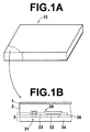
- Figure 1A is a perspective view showing the appearance of a radiation image sensor in accordance with a first embodiment of the present invention,
- Figure 1B is fragmentary cross-sectional view of a part of the radiation image sensor shown in Figure 1A,
- Figure 2 is a block diagram showing the radiation detector layer of the radiation image sensor shown in Figure 1A,
- Figure 3 is a view similar to Figure 1B but showing a part of a radiation image sensor in accordance with a second embodiment of the present invention,
- Figure 4 is a view similar to Figure 2 but showing a part of a radiation image sensor in accordance with a third embodiment of the present invention,
- Figure 5 is a plan view partly cut away showing a radiation image sensor in accordance with a fourth embodiment of the present invention,
- Figure 6 is a cross-sectional view showing a radiation image sensor in accordance with a fifth embodiment of the present invention, and
- Figure 7 is a cross-sectional view showing a radiation image sensor in accordance with a sixth embodiment of the present invention.
-
- In Figures 1A and 1B, a
radiation image sensor 10 of a first embodiment of the present invention comprises anelectrode layer 1 permeable to recording radiation, aradiation detector layer 2 which generates electric charges upon exposure to radiation passing through theelectrode layer 1 and an electricsignal detector layer 3 which detects as an electric signal the electric charges generated in theradiation detector layer 2. Thelayers 1 to 3 are superposed in this order. - The
radiation detector layer 2 comprises dispersion of radiation detector particles in polymer. The radiation detector particles may be of, for instance, HgI2, PbI2, Cd1-xZnxTe, TIBr, PbO, Pb2O3, BiI3 or BiGeO. The polymer may comprise, for instance, polyester, acrylic polymer or nylon polymer. Suitably the ratio of the radiation detector particles is in the range of 1/5 to 1/100 by weight. Since being good in film-forming properties, the above listed polymer can form aradiation detector layer 2 in a small amount and can form aradiation detector layer 2 high in mechanical strength. - As shown in Figure 1B, the electric
signal detector layer 3 comprises a number ofdetector elements 35, each of which comprises aTFT switch 31, apixel capacity cell 32 and apixel electrode 33, which are two-dimensionally arranged on aplastic substrate 34 . TheTFT switch 31 is formed by an organic TFT, a ZnO TFT or a poly-Si TFT produced by low-temperature film forming. Also thepixel capacity cell 32 and thepixel electrode 33 are formed of material which can form film at low temperature. Thepixel capacity cell 32 and thepixel electrode 33 form a capacitor together with aninsulating layer 36. Theplastic substrate 34 may be of polycarbonate, polyester, polyethylene naphthalate (PEN) or polyimide. - In Figure 2, electric charges generated in the
radiation detector layer 2 upon exposure to radiation are stored in the capacitor formed by thepixel capacity cell 32, thepixel electrode 33 and theinsulating layer 36. TheTFT switch 31 is turned on and off by a control signal generated by a gatescanning line drive 50 by way of agate scanning line 51, whereby electric charges stored in the capacitor connected to eachTFT switch 31 are read out. The signal thus read out is output through asignal line 52, anamplifier 53,multiplexer 54 and an A/D convertor 55. - The
radiation detector layer 2 may be formed on the surface of the electric signal detector layer by directly coating the surface of the electric signal detector layer with dispersion of radiation detector particles in polymer by the use of a blade coater, a slit coater or the like. - The
electrode layer 1 is formed by vapor deposition, coating or the like of electrode material such as Al or Au on the surface of theradiation detector layer 2 formed by coating. - A radiation image sensor in accordance with a second embodiment of the present invention will be described, hereinbelow, with reference to Figure 3.
- In Figure 3, the
radiation image sensor 20 of the second embodiment comprises aradiation detector sheet 25 comprising aradiation detector layer 23 formed by coating with dispersion of radiation detector particles in polymer aplastic substrate 21 carrying thereon anelectrode layer 22 permeable to recording radiation and an electricsignal detector layer 3 which detects as an electric signal the electric charges generated in theradiation detector layer 23. The electricsignal detector layer 3 is of the same structure as that employed in the first embodiment. The electricsignal detector layer 3 and theradiation detector sheet 25 are laminated one on the other by way ofconductive resin film 40. - The
plastic substrate 21 of theradiation detector sheet 25 may be formed of the same material as theplastic substrate 34 employed in the first embodiment. Theelectrode layer 22 is formed by coating theplastic substrate 21 with conductive material. Theplastic substrate 21 may be coated with the dispersion in the manner described above in conjunction with the first embodiment. Acharge collector electrode 24 is provided on the surface of theradiation detector sheet 25 opposed to a pixel on the electricsignal detector layer 3. - The
conductive resin film 40 comprises conductive resin film fractions each provided on the surface of one of thepixel electrodes 33 of the electricsignal detector layer 3 to electrically connect thepixel electrode 33 to the opposedcharge collector electrode 24. - When producing a
radiation image sensor 20 of this embodiment, the surface of the electricsignal detector layer 3 is coated with photosensitive material which contains conductive material and can be patterned by photolithography and the photosensitive material is dried into film. Otherwise, film of photosensitive material containing therein photosensitive material is applied to the surface of the electricsignal detector layer 3. Thenconductive resin film 40 of a pattern opposed to a predetermined area of each pixel electrode 33 (formed by the conductive resin film fractions which are arranged in a pattern opposed to a predetermined area of each pixel electrode 33) is formed by photolithography. - The
radiation detector sheet 25 is separately formed, and theradiation detector sheet 25 and the electricsignal detector layer 3 are laminated by hot pressing with the conductive resin film fractions opposed to thecorresponding pixel electrodes 33. - As can be understood from the description above, the
radiation image sensors radiation image sensors radiation image sensors - Though, in the first and second embodiments described above, the
detector element 35 for detecting electric charges comprises aTFT switch 31, the detecting element need not be limited to such element but may comprise, for instance, a capacitor and a switching diode as shown in Figure 4. That is, the radiation image sensor in accordance with a third embodiment of the present invention shown in Figure 4 includesdetector elements 60 each comprising acapacitor 61 and a switchingdiode 62. The electric charges stored in thecapacitors 61 are read out as an electric signal by controlling the electric potential at acontrol line 63 by aline decoder 64, thereby controlling the switchingdiodes 62. - The structure of the electric circuit of the electric
signal detector layer 3 need not be limited to those described above but may be various so long as it can be formed on a plastic substrate by low-temperature film forming. - The
radiation image sensors casing 70 formed of light-shielding material which is small in X-ray absorption. Thecasing 70 comprising a box-like body 70a open at its upper side and alid 70b which closes the upper side of thebody 70a. Thelid 70b is removably mounted on thebody 70a so that the radiation image sensors 10 (20) housed in thecasing 70 can be changed. - The
radiation image sensor 10 in accordance with the first embodiment of the present invention can be integrated with a casing as shown in Figure 6. That is, theelectrode layer 1 is formed on the surface of alid 80a of a casing with thelid 80a used as the substrate. - Further, an
X-ray absorbing layer 90 may be formed on the bottom of acasing body 80b to absorb radiation passing through aradiation image sensor 10 so that the radiation cannot affect another radiation image sensor as backscattered radiation. TheX-ray absorbing layer 90 may be formed of Pb, W, Ta or compounds of these metals. Thecasing 70 shown in Figure 5 may be provided on the bottom of itsbody 70a with an X-ray absorbing layer.
Claims (6)
- A radiation image sensor comprising
a radiation detector layer formed of radiation detector particles which generate electric charges upon exposure to recording radiation and are dispersed in a polymer, and
an electric signal detector layer formed of detector elements each of which is formed on the surface of a plastic substrate for each pixel to detect the electric charges generated at the corresponding pixel in the radiation detector layer,
wherein the radiation detector layer and the electric signal detector layer are laminated one on the other. - A radiation image sensor as defined in Claim 1 in which the radiation detector layer and the electric signal detector layer are laminated one on the other by way of conductive resin film partitioned for respective pixels.
- A radiation image sensor as defined in Claim 1 or 2 in which the radiation detector particles are of HgI2, PbI2, Cd1-xZnxTe, TIBr, PbO, Pb2O3, BiI3 or BiGeO.
- A radiation image sensor as defined in any one of Claims 1 to 3 in which the polymer comprises polyester, acrylic polymer or nylon polymer.
- A method of producing a radiation image sensor defined in Claim 1 comprising the step of
forming the radiation detector layer by coating with dispersion of the radiation detector particles in polymer the side of the electric signal detector layer on which the detector elements are formed. - A method of producing a radiation image sensor as defined in Claim 2 comprising the steps of
forming conductive resin film on each of the detector elements on the electric signal detector layer and laminating the electric signal detector layer provided with conductive resin film on each of the detector elements on the radiation detector layer.
Applications Claiming Priority (2)
| Application Number | Priority Date | Filing Date | Title |
|---|---|---|---|
| JP2002269723 | 2002-09-17 | ||
| JP2002269723A JP2004111511A (en) | 2002-09-17 | 2002-09-17 | Radiograph detector and its manufacturing method |
Publications (1)
| Publication Number | Publication Date |
|---|---|
| EP1400817A1 true EP1400817A1 (en) | 2004-03-24 |
Family
ID=31944514
Family Applications (1)
| Application Number | Title | Priority Date | Filing Date |
|---|---|---|---|
| EP03020960A Withdrawn EP1400817A1 (en) | 2002-09-17 | 2003-09-16 | Radiation image sensor and method of producing the same |
Country Status (3)
| Country | Link |
|---|---|
| US (1) | US20040051047A1 (en) |
| EP (1) | EP1400817A1 (en) |
| JP (1) | JP2004111511A (en) |
Cited By (1)
| Publication number | Priority date | Publication date | Assignee | Title |
|---|---|---|---|---|
| US7507512B2 (en) | 2005-11-29 | 2009-03-24 | General Electric Company | Particle-in-binder X-ray sensitive coating using polyimide binder |
Families Citing this family (4)
| Publication number | Priority date | Publication date | Assignee | Title |
|---|---|---|---|---|
| GB0103133D0 (en) * | 2001-02-08 | 2001-03-28 | Univ Glasgow | Improvements on or relating to medical imaging |
| JP5366906B2 (en) * | 2010-08-26 | 2013-12-11 | 富士フイルム株式会社 | Radiography equipment |
| CN102385062A (en) * | 2010-08-26 | 2012-03-21 | 富士胶片株式会社 | Radiation shooting device |
| CN105811953B (en) * | 2016-04-21 | 2019-05-28 | 山东师范大学 | Application of the diiodinating thin film lead in subpicosecond entirely optomagnetic switch |
Citations (2)
| Publication number | Priority date | Publication date | Assignee | Title |
|---|---|---|---|---|
| EP0898421A2 (en) * | 1997-08-19 | 1999-02-24 | Fuji Photo Film Co., Ltd. | Electrostatic recording member, electrostatic latent image recording apparatus, and electrostatic latent image read-out apparatus |
| US5886359A (en) * | 1996-06-13 | 1999-03-23 | Eastman Kodak Company | X-ray dectector, detection assembly, and method |
Family Cites Families (4)
| Publication number | Priority date | Publication date | Assignee | Title |
|---|---|---|---|---|
| US5556716A (en) * | 1994-08-25 | 1996-09-17 | E. I. Du Pont De Nemours And Company | X-ray photoconductive compositions for x-ray radiography |
| JP4040879B2 (en) * | 2000-01-11 | 2008-01-30 | 浜松ホトニクス株式会社 | X-ray image detector |
| US6717173B2 (en) * | 2000-02-08 | 2004-04-06 | Fuji Photo Film Co., Ltd. | Radio-conductive material, method of manufacturing the same, solid sensor using the same, method of manufacturing radio-conductive film, and radiation image read-out apparatus |
| JP2002162474A (en) * | 2000-11-27 | 2002-06-07 | Sharp Corp | Electromagnetic wave detector and method of manufacturing the same |
-
2002
- 2002-09-17 JP JP2002269723A patent/JP2004111511A/en active Pending
-
2003
- 2003-09-16 EP EP03020960A patent/EP1400817A1/en not_active Withdrawn
- 2003-09-16 US US10/662,328 patent/US20040051047A1/en not_active Abandoned
Patent Citations (2)
| Publication number | Priority date | Publication date | Assignee | Title |
|---|---|---|---|---|
| US5886359A (en) * | 1996-06-13 | 1999-03-23 | Eastman Kodak Company | X-ray dectector, detection assembly, and method |
| EP0898421A2 (en) * | 1997-08-19 | 1999-02-24 | Fuji Photo Film Co., Ltd. | Electrostatic recording member, electrostatic latent image recording apparatus, and electrostatic latent image read-out apparatus |
Non-Patent Citations (1)
| Title |
|---|
| DE MONTS H ET AL: "A NEW PHOTOCONDUCTOR IMAGING SYSTEM FOR DIGITAL RADIOGRAPHY", MEDICAL PHYSICS, AMERICAN INSTITUTE OF PHYSICS. NEW YORK, US, vol. 16, no. 1, 1989, pages 105 - 109, XP000256758, ISSN: 0094-2405 * |
Cited By (1)
| Publication number | Priority date | Publication date | Assignee | Title |
|---|---|---|---|---|
| US7507512B2 (en) | 2005-11-29 | 2009-03-24 | General Electric Company | Particle-in-binder X-ray sensitive coating using polyimide binder |
Also Published As
| Publication number | Publication date |
|---|---|
| JP2004111511A (en) | 2004-04-08 |
| US20040051047A1 (en) | 2004-03-18 |
Similar Documents
| Publication | Publication Date | Title |
|---|---|---|
| US9520438B2 (en) | Electromagnetic wave detecting element | |
| JP5448877B2 (en) | Radiation detector | |
| EP1911094B1 (en) | Radiation detecting apparatus and radiation detecting system | |
| US7521684B2 (en) | Radiation detecting apparatus, manufacturing method therefor, and radiation image pickup system | |
| US5381014A (en) | Large area X-ray imager and method of fabrication | |
| US8044360B2 (en) | Radiation detector | |
| US6600158B1 (en) | Semiconductor device and radiation image pickup system having the device | |
| US7233021B2 (en) | Active matrix substrate, electromagnetic detector, and liquid crystal display apparatus | |
| TWI227562B (en) | Photoelectric conversion device, image scanning apparatus, and manufacturing method of the photoelectric conversion device | |
| EP1400817A1 (en) | Radiation image sensor and method of producing the same | |
| WO2019176137A1 (en) | Radiation detection panel, radiation detector, and method for manufacturing radiation detection panel | |
| JP2007170908A (en) | Radiation detector and imaging apparatus using the same | |
| WO2000002255A1 (en) | Direct radiographic imaging panel having a dielectric layer with an adjusted time constant | |
| JP2014122903A (en) | Radiation detector and radiation imaging device | |
| JP2005308582A (en) | Radiation detector | |
| JP2005308583A (en) | Radiation detector | |
| JP2002311145A (en) | Radiation detector | |
| US8193510B2 (en) | Radiation detector | |
| JP4545538B2 (en) | Photoconductive layer and radiation imaging panel constituting radiation imaging panel | |
| JP2007093257A (en) | Radiation detector | |
| JP2005274259A (en) | Manufacturing method for photoconductive layer constituting radiation imaging panel | |
| JP2010056431A (en) | Method of manufacturing radiation detector | |
| JP2007005625A (en) | Photoconduction layer which constitutes radiation image pick-up panel and radiation image pickup panel | |
| JP2006093582A (en) | Radiation imaging panel and photoconduction layer constituting the same | |
| JP2005276975A (en) | Manufacturing method of photoconductive layer constituting radiation imaging panel |
Legal Events
| Date | Code | Title | Description |
|---|---|---|---|
| PUAI | Public reference made under article 153(3) epc to a published international application that has entered the european phase |
Free format text: ORIGINAL CODE: 0009012 |
|
| AK | Designated contracting states |
Kind code of ref document: A1 Designated state(s): AT BE BG CH CY CZ DE DK EE ES FI FR GB GR HU IE IT LI LU MC NL PT RO SE SI SK TR |
|
| AX | Request for extension of the european patent |
Extension state: AL LT LV MK |
|
| 17P | Request for examination filed |
Effective date: 20040423 |
|
| AKX | Designation fees paid |
Designated state(s): BE DE FR NL |
|
| RAP1 | Party data changed (applicant data changed or rights of an application transferred) |
Owner name: FUJIFILM CORPORATION |
|
| STAA | Information on the status of an ep patent application or granted ep patent |
Free format text: STATUS: THE APPLICATION HAS BEEN WITHDRAWN |
|
| 18W | Application withdrawn |
Effective date: 20090210 |