-
The present invention generally relates to a method for processing
film stacks. More specifically, the invention relates to a method for removal of
residue after plasma etching a film stack using a mask.
-
Microelectronic devices are generally fabricated on a semiconductor
substrate as integrated circuits. An example of such a device is a magneto-resistive
random access memory (MRAM) wherein magnetic multilayer films, or
film stacks, are used as storage elements. The magnetic multi-layer films are
typically a stack of different layers composed of various materials, for example
permalloy (NiFe), cobalt iron (CoFe), tantalum (Ta), copper (Cu) and the like,
and may also contain insulator materials such as aluminum oxide as a thin
tunneling layer sandwiched between the multi-layers. The layers are typically
deposited in overlying blanket films, layer by layer, and then featured. One of
the typical processes used during feature fabrication is plasma etching, in which
one or more layers comprising a film stack are removed, either partially or in
total to form a feature.
-
During the plasma etching process, a metal film (or film stack) is
etched using a plasma, for example a plasma comprising fluorine or chlorine
chemistry. In such an example, the fluorine or chlorine from the etchant
combines with the removed metal to form a residue. For example, if a film
contains tantalum, a plasma etch process utilizing chlorine (Cl2) will form
tantalum chloride (TaCl) residue. Additionally, if a carbon-based photoresist is
used during metal etching, a metal-containing polymer may also form as an
additional residue resulting from the etch process.
-
The residues typically deposit or redeposit along the sidewalls of the
layer or film stack. These residues, for example, can be redeposition of the
material just removed from the layer along the sidewalls of the film or film stack.
Additionally, the residues may include a by-product of the plasma etchant
reacting with the removed metal and this by-product residue being deposited
along the sidewalls of the film or film stack. Such residues may build up along
the sides of the film or film stack above the upper surface of the film or film
stack, forming a "veil" like structure.
-
Residues containing metal, metal chlorides, fluorides, oxides and
polymers interfere with further processing of the film or film stack. These
residues may contaminate any additional films or layers that are deposited upon
the remaining metal and/or the film or film stack. Additionally, the residues, and
especially the veil-like structures, can cause electrical short-circuits, for example
as between the two magnetic layers separated by a thin tunneling layer within a
MRAM device, and other problems, as well as causing film stack
irreproducibility.
-
Therefore, there is a need in the art for a method of removing
residues after plasma etching a film stack.
-
The disadvantages of the prior art are overcome by a method for
removal of residue after plasma etching a magneto-resistive random access
memory (MRAM) film stack. The film stack contains a photoresist layer, a hard
mask layer, a conductive layer, a layer or layers of magnetic material and a
tunneling layer. The hard mask layer is used in conjunction with the photoresist
layer as a dual mask for etching a layer or layers of magnetic material.
Following an etching of the hard mask layer and conductive layer using
chlorine-based or fluorine based chemistry, the residues, including the presence
of any "veil"-like structures, are removed using a wet dip in a mixture of
ammonium hydroxide, hydrogen peroxide and water.
The present invention intends to overcome at least some of the above problems. The object is
solved by the methods according to claim I and claim 2.
-
Further advantages, features, and aspects and details of the invention are evident from the
dependent claims, the description and the accompanying drawings.
-
The present invention generally relates to a method for removal of residue after plasma
etching a film stack. The film stack preferably contains a photoresist layer, a hard mask layer,
a conductive layer, a layer or layers of magnetic material and/or a tunneling layer. The hard
mask layer, preferably, is used in conjunction with the photoresist layer as a dual mask for
etching a layer or layers of magnetic material.
-
Following an etching of the hard mask layer and conductive layer, preferably by using
chlorine-based or fluorine based chemistry, the residues, including the presence of any "veil"-like
structures, are removed, preferably by using a wet dip in a mixture of ammonium
hydroxide, hydrogen peroxide and, preferably, water.
-
Further, the method according to the invention refers to a method for removal of residue after
plasma etching a film stack, preferably comprising a patterned photoresist material layer, a
hard mask layer, a conductive layer, and a magnetic layer, wherein the patterned photoresist
material layer and the hard mask layer form a dual mask. The method cleans a substrate
containing the film stack after the dual mask of the film stack has been etched to remove
residue produced during etching the process. Preferably, the cleaning step is performed in a
solution comprising hydrogen peroxide and ammonium hydroxide that removes the residue.
-
Preferably, the method for removal of residue after plasma etching a film stack, according to
the invention, is carried out by using a photoresist/silicon dioxide dual mask.
-
Further, preferably, the film stack is a magneto-resistive random access memory (MRAM)
film stack.
-
So that the manner in which the above recited features of the present
invention are attained and can be understood in detail, a more particular
description of the invention, briefly summarized above, may be made by
reference to the embodiments thereof which are illustrated in the appended
drawings.
-
Figure 1 depicts a schematic cross-sectional view of a substrate
having a film stack;
-
Figures 2-5 depict a schematic cross-sectional views of a film stack of
Figure 1 after intermediate processing steps in accordance with one example of
the inventive method;
-
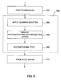
Figure 6 depicts a flow diagram of an example of the inventive
method;
-
Figure 7 depicts a schematic, cross sectional view of an illustrative
wet dip cleaning module;
-
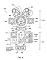
Figure 8 depicts a schematic view of an illustrative platform for
performing the method of the present invention; and
-
Figure 9 depicts a schematic, cross sectional view of an illustrative
etch module.
-
To facilitate understanding, identical reference numerals have been
used, where possible, to designate identical elements that are common to the
figures.
-
It is to be noted, however, that the appended drawings illustrate only
typical embodiments of this invention and are therefore not to be considered
limiting of its scope, for the invention may admit to other equally effective
embodiments.
-
In one preferred embodiment, the present invention relates to a
method for removal of residue produced by plasma etching a magneto-resistive
random access memory (MRAM) film stack.
The film stack contains a photoresist layer, an anti-reflective coating layer, a
hard mask layer, a conductive layer, a layer or layers of magnetic material and
a tunneling layer. The film stack may contain additional layers to form a
complete MRAM device. The hard mask layer is used in conjunction with the
photoresist and the anti-reflective coating layer, as a dual mask for etching a
layer or layers of magnetic material to the tunneling layer. Following a chlorine-based
or fluorine-based chemistry etching of the hard mask layer and
conductive layer, the residues, including the presence of any "veil"-like
structures, are removed using a wet dip in a mixture of ammonium hydroxide,
hydrogen peroxide and water.
-
Figure 1 is a schematic cross-sectional view of a substrate 100 before
the photoresist strip and plasma etching. In this example, the substrate 100
comprises a film stack 102. The film stack comprises a photoresist layer 104,
an anti-reflective coating layer 106 (a bottom anti-reflective coating or BARC),
hard mask layer 108, conductive layer 110, magnetic layers 112, 114,
separated by a thin tunneling layer 116. Layers 112, 114 and 116 form a
magnetic tunnel junction 118.
-
The layer 104 of photoresist material is conventionally processed
using a lithographic patterning routine, i.e., the photoresist is applied to a
surface of the wafer, exposed through a mask, and developed. The developed
photoresist is generally a carbon-based polymer that remains only on top of the
stack 102 in the areas that are to be protected during plasma etch. As the
feature size of the lithographic pattern is reduced, inaccuracies in the pattern
transfer process can arise from optical limitations inherent in the lithographic
process, for example light reflection. The bottom anti-reflective coating layer
106 (or BARC) positioned between the underlying hard mask layer 108 and the
photoresist layer 104 controls the reflection of light from the underlying metal or
metal-containing layers. In some instances a BARC layer is not used. As such,
the BARC layer is considered optional. The anti-reflective coating layer is
typically composed of various materials, including organic and inorganic
materials, and may include, for example, inorganic materials such as silicon
nitride, silicon oxynitride, titanium nitride, silicon carbide, and the like, and
organic materials such as polyamides and polysulfones. Together, layers 104
and 106 have a thickness of about 6000 Angstroms.
-
The underlying hard mask layer 108 is formed from, for example,
silicon dioxide and boron or phosphorus doped or undoped silicon dioxide, and
has a thickness of about 500 Angstroms. Other hard mask materials (e.g., SiN,
SiON, and the like) that are known in the art may also be used. Together, the
photoresist layer 104, the anti-reflective layer 106 and the silicon oxide layer
108 form a dual mask 109.
-
The conductive layer 110 is formed, for example, from either tantalum
(Ta) or tantalum nitride (TaN) and has a thickness of about 300-600 Angstroms.
The magnetic layers 112 and 114 are formed from, for example, magnetic
materials such as nickel and cobalt iron alloys, such as CoFe, NiFe and the like,
and each layer may consist of one or more sub-layers of a combination of these
alloys. The magnetic layers 112 and 114 have a thickness of about 50-100
Angstroms for layer 112 and of about 300-400 Angstroms for layer 114. The
thin tunneling layer 116 is composed of an insulating material, such as for
example alumina (Al2O3) and has a thickness, for example, of about 10-15
Angstroms.
-
Figure 2 is a schematic cross-sectional view of the film stack 102
after plasma etching is completed. Either chlorine-based or fluorine-based
conventional chemistries, such as for example Cl2, HCl, CF4 or CHF3, can be
used during plasma etching of the conductive layer metals such as tantalum or
tantalum nitride. Plasma etching can be performed in a Decoupled Plasma
Source (DPS) II module of the Centura® metal etch system, available from
Applied Materials, Inc. of Santa Clara, California. The DPS II module uses a 2
MHz inductive plasma source to generate and sustain high density plasma. A
wafer is biased by a 13.56 MHz bias source. The decoupled nature of the
plasma source allows independent control of ion energy and ion density. The
DPS II module provides a wide process window over changes in source and
bias power, pressure, and etch gas chemistry and uses an endpoint system to
determine an end of the etch process. The DPS II module is discussed in detail
with respect to Figure 9 below.
-
During a first plasma etching of the film stack 102, some amount of
the metal (e.g., tantalum) from the layer 110 is etched from the stack and
becomes deposited on the top and sidewalls of the photoresist layer 104. The
anti-reflective coating layer 106 and the hard mask layer 108 not covered by the
photoresist layer 104 are also etched and materials from these layers may also
become deposited on the top and sidewalls of the photoresist layer 104. The
photoresist layer 104 may also be partially dissolved by the etchant. During the
etch process, the etched metal combines with the components of the etchant
(for example, chlorine or fluorine) as well as with components of the photoresist
and may also combine with the etched components of the anti-reflective coating
layer 106 and hard mask layer 108. A residue 124 containing, for example,
metal, metallic-chloride or metallic-fluoride as well as metal-containing
polymers, as well as other possible combinations from the etched anti-reflective
coating and hard mask layer components, is deposited on the sidewalls 120
and 122 of the film stack 102 or elsewhere on the substrate. As a result of this
residue generation, after the first plasma etching, residue 124 remains on the
sidewalls 120 and 122, but also may remain and extend above the surface of
the top-most layer, the photoresist layer 104, to form a veil 126. The residue is
considered a contaminant with respect to further processing of the substrate.
-
The residue 124 is removed by post-first plasma-etch processing the
substrate in a wet dip solution comprising ammonium hydroxide, hydrogen
peroxide and water. Figure 3 depicts a schematic cross-sectional view of the
film stack 102 after the wet dip in accordance with one example of the present
invention. As shown, the wet dip has removed the etch residue.
-
The photoresist material in layer 104 and anti-reflective coating
material in layer 106 are then removed by conventional photoresist stripping
techniques, such as for example, plasma stripping and passivation processes or
wet chemical etching. Figure 4 depicts a schematic cross-sectional view of the
film stack 102 after photoresist stripping of photoresist layer 104 and anti-reflective
coating layer 106.
-
Figure 5 is a schematic cross-sectional view of the film stack 102
after a oxygen and chlorine-mixed chemistry plasma etch, i.e. a second plasma
etch, is completed in accordance with one example of the present invention.
Any oxygen-based and chlorine-based chemistries, such as for example oxygen
and chlorine plasma, may be utilized during etching of the magnetic layer 112 to
the thin tunneling layer 116. The tunneling layer 116 can be used as an etch
stop layer. The hard mask layer 108 forms a hard mask that protects the
underlying layers of the film stack 102, thus permitting high selectivity and
etching of the second plasma etch to the tunneling layer.
-
During the oxygen and chlorine-mixed chemistry etch of the film stack
as depicted in Figure 5, the hard mask layer 108 and the conductive layer 110
are not etched and act together as a hard mask over the underlying layers 112,
114 and 116. The magnetic layer 112 not covered by the mask of layer 108
and the conductive layer 110 is etched. The hard mask layer 108 remains
smooth and substantially residue free after the oxygen and chlorine-mixed
chemistry etch.
-
Figure 6 is a flow diagram of an example of one embodiment of the
inventive method 602 for post-plasma-etch processing the substrate to remove
etch residue. At step 600, a film stack that comprises a layer or layers of metals
undergoes a first plasma etching. During step 600, a residue forms on the side
walls of the film stack or elsewhere on the substrate. In one embodiment of the
first plasma etch of step 600, the wafer temperature was about 10 to 80
degrees Celsius, pressure and flow of the reactant gases CF4 and CHF3 were
about 1 to 30mTorr and 10 to 200 sccm of each gas and plasma excitation
power was about 200 to 300 Watts. Argon is used as a diluent at a flow rate of
about 10 to 200 sccm. The cathode pedestal bias power was about 0 to 500
Watts. One specific recipe used in a DPS II module provides 60 sccm of CF4,
20 sccm of CHF3, 60 sccm of Ar, applying 1000 Watts of plasma excitation
power and 50 Watts of cathode pedestal bias power, and maintaining the
substrate temperature at 40 degrees Celsius and a pressure in the reactor of 10
mTorr.
-
At step 604, the substrate is dipped in a solvent to remove the
residue in accordance with one embodiment of the invention. In one
embodiment, the solvent solution of step 604 comprises hydrogen peroxide,
ammonium hydroxide and deionized water. In particular, the ratio of the
ammonium hydroxide to hydrogen peroxide to deionized water ranges from
about 1 to 1 to 10 to about 0.1 to 1 to 10 by volume. Duration of the cleaning
step is generally between about 1 to about 2 minutes, though longer cleaning
periods may be used. During cleaning, the solvent solution has a temperature of
about 45 to 75 degrees Celsius. In one specific example, the solvent solution
has a temperature of 65 degrees Celsius and the duration of the cleaning step
is 2 minutes.
-
After step 604, the photoresist and underling anti-reflective coating
layer are removed by step 606, leaving a hard mask layer as the top layer of the
film stack. The plasma stripping of the photoresist and anti-reflective coating
layers of step 604 is a process generally performed using a microwave
downstream, oxygen plasma reactor. The process can be performed in the
Advanced Strip and Passivation (ASP) module of the Centura® metal etch
system, available from Applied Materials, Inc. of Santa Clara, California. The
ASP module is a microwave downstream oxygen plasma reactor in which the
plasma is confined to a plasma tube and only reactive neutrals are allowed to
enter a process chamber. Such a plasma confinement technique precludes
plasma-related damage of the substrate or circuits formed on the substrate. In
the ASP module, wafer backside is heated radiantly by quartz halogen lamps
and the wafer temperature can be maintained between about 200 to about 300
degrees Celsius.
-
In one embodiment of the invention, the photoresist and BARC layers
are removed in the ASP module by supplying between 500 and 5000 sccm of
O2, between 0 and 1000 sccm of N2, applying between 200 to 3000 Watts to
excite a plasma, and maintaining a wafer temperature between 150 to 400
degrees Celsius and a pressure in the reactor between 1 to 10 Torr. In this
embodiment of the invention, good results were observed with the oxygen-based
reactant gas. One specific process recipe provides 3500 sccm of O2,
300 sccm of N2, applies 1400 Watts to excite a plasma, and maintains a wafer
temperature at 200 degrees Celsius and a pressure in the reactor at 2 Torr.
-
The photoresist stripping can also be performed in-situ in the DPS II
module. In one embodiment of the invention, in the DPS II chamber, the
photoresist and BARC layers are removed by supplying between 50 and 200
sccm of O2, between 0 and 50 sccm of N2, applying power to an inductively
coupled antenna about 1000 Watts, applying a cathode electrode bias power
about 10 Watts, and maintaining a wafer temperature about 40 degrees Celsius
and a pressure in the reactor about 30 mTorr for a duration of about 120
seconds. In this embodiment of the invention, a duration of the stripping
process may be between 1 and 8 minutes.
-
Following step 606, the film stack undergoes step 608 wherein a
second plasma etching is performed using oxygen and chlorine-mixed
chemistries. During step 608, a second residue forms on the side walls of the
film stack or elsewhere on the substrate. In one embodiment of the invention,
the magnetic layer 112 is etched in the DPS II module by supplying between 10
and 50 sccm of O2, between 10 and 100 sccm of Cl2, between 10 and 100 sccm
of Ar, applying power to an inductively coupled antenna between 200 to 3000
Watts, applying a cathode electrode bias power between 0 to 300 Watts, and
maintaining a wafer temperature between 40 to 500 degrees Celsius and a
pressure in the reactor between 1 to 2 mTorr. One specific process recipe
provides 20 sccm of O2, 40 sccm of Cl2, 20 sccm of Ar, applying 900 Watts to
the antenna and 100 Watts to the cathode electrode, and maintaining a wafer
temperature at 40 degrees Celsius and a pressure in the reactor at 5 mTorr.
-
At step 610, a deionized (DI) water rinse is performed to remove any
remaining traces of residue. The result is an MRAM film stack etched to the
tunneling layer.
-
FIG. 9 depicts a schematic diagram of the DPS II etch reactor 900 that
may be uses to practice the inventive method. The process chamber 910
comprises at least one inductive coil antenna segment 912, positioned exterior
to a dielectric ceiling 920. Other modifications may have other types of ceilings,
e.g., a dome-shaped ceiling. The antenna segment 912 is coupled to a
radio-frequency (RF) source 918 that is generally capable of producing an RF
signal having a tunable frequency of about 50 kHz and 13.56 MHz. The RF
source 918 is coupled to the antenna 912 through a matching network 919.
Process chamber 910 also includes a wafer support pedestal (cathode) 916 that
is coupled to a source 922 that is generally capable of producing an RF signal
having a frequency of approximately 13.56 MHz. The source 922 is coupled to
the cathode 916 through a matching network 924. Optionally, the source 922
may be a DC or pulsed DC source. The chamber 910 also contains a
conductive chamber wall 930 that is connected to an electrical ground 934. A
controller 940 comprising a central processing unit (CPU) 944, a memory 942,
and support circuits 946 for the CPU 944 is coupled to the various components
of the DPS etch process chamber 910 to facilitate control of the etch process.
-
In operation, the semiconductor wafer 914 is placed on the wafer support
pedestal 916 and gaseous components are supplied from a gas panel 938 to
the process chamber 910 through entry ports 926 to form a gaseous mixture
950. The gaseous mixture 950 is ignited into a plasma 955 in the process
chamber 910 by applying RF power from the RF sources 918 and 922
respectively to the antenna 912 and the cathode 916. The pressure within the
interior of the etch chamber 910 is controlled using a throttle valve 927 situated
between the chamber 910 and a vacuum pump 936. The temperature at the
surface of the chamber walls 930 is controlled using liquid-containing conduits
(not shown) that are located in the walls 930 of the chamber 910.
-
The temperature of the wafer 914 is controlled by stabilizing the
temperature of the support pedestal 916 and flowing helium gas from source
948 to channels formed by the back of the wafer 914 and grooves (not shown)
on the pedestal surface. The helium gas is used to facilitate heat transfer
between the pedestal 916 and the wafer 914. During the processing, the wafer
914 is heated by a resistive heater within the pedestal to a steady state
temperature and the helium facilitates uniform heating of the wafer 914. Using
thermal control of both the ceiling 920 and the pedestal 916, the wafer 914 is
maintained at a temperature of between 0 and 500 degrees Celsius. The RF
power applied to the inductive coil antenna 912 has a frequency between 50
kHz and 13.56 MHz and has a power of 200 to 2500 Watts. The bias power of
between 0 and 300 Watts is applied to the pedestal 916 may be in a form of a
DC, pulsed DC, or RF power.
-
To facilitate control of the chamber as described above, the CPU 944
may be one of any form of general purpose computer processor that can be
used in an industrial setting for controlling various chambers and sub-processors.
The memory 942 is coupled to the CPU 944. The memory 942, or
computer-readable medium, may be one or more of readily available memory
such as random access memory (RAM), read only memory (ROM), floppy disk,
hard disk, or any other form of digital storage, local or remote. The support
circuits 946 are coupled to the CPU 944 for supporting the processor in a
conventional manner. These circuits include cache, power supplies, clock
circuits, input/output circuitry and subsystems, and the like. The inventive
method is generally stored in the memory 942 as software routine. The
software routine may also be stored and/or executed by a second CPU (not
shown) that is remotely located from the hardware being controlled by the CPU
944.
-
One illustrative embodiment of an apparatus that can be used for
cleaning and rinsing a substrate in accordance with the present invention is a
single substrate wet cleaning module. FIG. 7 depicts a simplified cross-sectional
view of an illustrative embodiment of a single substrate wet cleaning
module 700. The module 700 is described in detail in US patent application
serial number 09/945,454, filed August 31, 2001 (attorney docket number
4936), which is herein incorporated by reference.
-
The module 700 applies cleaning chemicals and/or rinsing agents to
the top and bottom of a substrate. To enhance the cleaning process, the
module 700 uses acoustic or sonic waves to agitate the cleaning chemicals
and/or rinsing agents.
-
The module 700 comprises a chamber 701, a nozzle 714, and a
substrate support 712. The substrate support is mounted within the chamber
701 and comprises edge claps 710, plate 702 and a plurality of acoustic or
sonic transducers 704. The plate 702 has a shape that is substantially the
same as a substrate and supports the plurality of acoustic or sonic transducers
704. The plate 702 is, for example, made of aluminum, but can be formed of
other materials such as, but not limited to, stainless steel and sapphire. The
plate 702 is coated with a corrosion resistant fluoropolymer such as HALAR or
PFA. The transducers 704 are attached to the bottom of the plate 702 using an
adhesive, for example, an epoxy 706. In one embodiment of the cleaning
module 700, the transducers 704 are arranged in an array that covers
substantially the entire bottom surface of plate 702, e.g., approximately 80% of
plate 702. The transducers generate sonic waves in the frequency range
between 400 kHz and 8 MHz. In one embodiment of the module 700, the
transducers are piezoelectric devices.
-
The plurality of edge clamps 710 retain the substrate 708 face up
above the plate 708 to form a gap 718 between the backside of the wafer and
the top surface of the plate 702. The gap 718 is approximately 3mm. Cleaning
chemicals and/or rinsing agents are provides to the gap via channel 716. The
clamps are rotated to cause the substrate 708 to rotate about its central axis at
a rate between 0 and 6000 rpm. In this embodiment of module 700, the
substrate 708 and clamps 710 rotate, while the plate 702 is stationary.
-
The nozzle 714 sprays cleaning chemicals and/or rinsing agents upon
the top of the substrate 708 (i.e., the surface of the substrate comprising
features, transistors, or other circuitry). As the nozzle 714 sprays the top of the
substrate 708, the same or different cleaning chemicals and/or rinsing agents
are supplied to the gap 718 via channel 716 as the substrate is rotated such
that the cleaning chemicals and/or rinsing agents flow across the top and
bottom surfaces of the substrate.
-
The nozzle 714 and channel 716 are coupled to a source 724 of
cleaning chemicals and/or rinsing agents. The source 724 may be the same for
the nozzle 714 and channel 716, or a separate source may be couple to each of
the nozzle 714 and channel 716. In the present embodiment of the invention,
the module 700 is used to clean the substrate 708 using hydrogen peroxide,
ammonium hydroxide and deionized water. The module 700 is further used to
rinse the substrate in deionized water.
-
A computer controller 726 is generally used to control the operation of
the module 700. Specifically, the computer controller 726 controls the rotation
of the substrate support 712, the activation of the transducers 704, the supply of
cleaning chemicals and/or rinsing agents, and so on.
-
The method of the present invention (FIG. 6) is illustratively
performed on an integrated processing platform 800 shown in Fig. 8 that
comprises apparatus for performing both atmospheric and sub-atmospheric
processing. The platform 800 and the various modules and tools that can be
used with such a platform are described in detail in US patent application serial
number 09/945,454, filed August 31, 2001 (attorney docket number 4936),
which is herein incorporated by reference.
-
Depending upon the process modules that are used in the platform
800, the platform 800 (also referred to as a process tool) can be used to
perform etching, substrate cleaning, photoresist stripping, substrate inspection
and the like. The platform 800 comprises an atmospheric platform 802 and a
sub-atmospheric platform 804. The sub-atmospheric platform 804 and the
atmospheric platform 802 may be coupled together by a single substrate load
lock 806 or, as shown in the depicted example, are coupled together by a pair
of single load locks 806 and 808. In some applications, the sub-atmospheric
and atmospheric platforms 804 and 802 are not coupled together and may be
used separately. One such stand-alone platform configuration may contain
photoresist stripping modules and wet cleaning modules from providing a
platform that performs post-etch processing.
-
The atmospheric platform 802 comprises a central atmospheric
transfer chamber 810 containing a substrate handling device 812, such as a
robot. Directly attached to the atmospheric transfer chamber 810 is a substrate
wet cleaning module 850, an integrated particle monitor 852 and a critical
dimension (CD) measuring tool 854. A strip or dry clean module 817 can also
be attached to the atmospheric transfer chamber 810, if desired. Each module
or tool is coupled to the transfer chamber 810 by a separately closable and
sealable opening, such as a slit valve. The transfer chamber is maintained at
substantially atmospheric pressure during operation. The substrate handling
device 812 is able to transfer substrates from one module or tool to another
module or tool that is attached to the atmospheric transfer chamber 810. In the
embodiment shown, the substrate handling device 812 is a dual blade, single
arm, single wrist robot. Other types of robots may be used to access the
various modules and tools.
-
The atmospheric transfer chamber 810 is coupled to at least one
substrate input/output module 820 that provides and receives substrates to and
from the platform 800. In one embodiment of the platform 800, the module 820
comprises at least one front opening unified pod (FOUP). Two FOUPs 822 and
824 are depicted. The substrate handling device 812 accesses each FOUP
through a sealable access door 821. The substrate handling device 812 moves
linearly along a track 823 to facilitate access to all of the modules and tools.
-
The atmospheric transfer chamber 810 is coupled to the pair of load
locks 806 and 808 through sealable doors 805 and 809 such that the substrate
handling device 812 can access the load locks 806 and 808. The sub-atmospheric
platform 804 comprises a central sub-atmospheric transfer
chamber 830 and a plurality of process chambers 856, 858, 860, and 862.
Sealable doors 807 and 811 respectively couple each load lock 806 and 808 to
the sub-atmospheric transfer chamber 830. The sub-atmospheric transfer
chamber 830 contains a substrate handing device 832, such as a robot, that
accesses the load locks 806 and 808 as well as the process chambers 856,
858, 860 and 862. The process chambers 856, 858, 860 and 862 are each
coupled to the sub-atmospheric transfer chamber 830 via separately closable
and sealable openings, such as slit-valves. The process chambers 856, 858,
860 and 862 may comprise one or more etching chambers such as the DPS or
DPS II chamber that are available from Applied Materials, Inc. of Santa Clara,
California. Additionally, one or more photoresist stripping chambers such as the
ASP chamber described above may be used as one or more of the process
chambers 856, 858, 860 and 862. As also described above, the ASP chamber,
if used, may be located either on the sub-atmospheric platform 804 or the
atmospheric platform 802. FIG. 8 shows the sub-atmospheric platform 804
comprising two etch chambers 858 and 860 and two photoresist stripping
chambers 856 and 862. The sub-atmospheric platform 804 is, for example, a
CENTURA platform available for Applied Materials, Inc. of Santa Clara,
California.
-
The platform 800 also includes a system computer 870 that is
coupled to and controls each module that is coupled to the atmospheric and
sub-atmospheric platforms 802 and 804, controls the substrate handling
devices 812 and 832, and controls the load locks 806 and 808. Generally, the
system computer 870 controls all aspects of operation of the platform 800 either
by direct control of the sub-systems, modules, tools and apparatus or by
controlling the computers associated with those sub-systems, modules, tools
and apparatus. The system computer 870 enables feedback from one module
or tool to be used to control the flow of substrates through the platform 800
and/or control the processes or operation of the various modules and tools to
optimize substrate throughput.
-
The invention may be practiced in other semiconductor structures and
devices wherein the processing parameters may be adjusted to achieve
acceptable characteristics by those skilled in the art by utilizing the teachings
disclosed herein without departing from the spirit of the invention. While the
foregoing is directed to the preferred embodiment of the present invention, other
and further embodiments of the invention may be devised without departing
from the basic scope thereof, and the scope thereof is determined by the claims
that follow.