EP1398787A1 - Memory device having memory cell units each composed of a memory and complementary memory cell and reading method - Google Patents
Memory device having memory cell units each composed of a memory and complementary memory cell and reading method Download PDFInfo
- Publication number
- EP1398787A1 EP1398787A1 EP20030018821 EP03018821A EP1398787A1 EP 1398787 A1 EP1398787 A1 EP 1398787A1 EP 20030018821 EP20030018821 EP 20030018821 EP 03018821 A EP03018821 A EP 03018821A EP 1398787 A1 EP1398787 A1 EP 1398787A1
- Authority
- EP
- European Patent Office
- Prior art keywords
- memory cell
- complementary
- memory
- cell
- memory cells
- Prior art date
- Legal status (The legal status is an assumption and is not a legal conclusion. Google has not performed a legal analysis and makes no representation as to the accuracy of the status listed.)
- Granted
Links
Images
Classifications
-
- G—PHYSICS
- G11—INFORMATION STORAGE
- G11C—STATIC STORES
- G11C5/00—Details of stores covered by group G11C11/00
- G11C5/06—Arrangements for interconnecting storage elements electrically, e.g. by wiring
-
- G—PHYSICS
- G11—INFORMATION STORAGE
- G11C—STATIC STORES
- G11C11/00—Digital stores characterised by the use of particular electric or magnetic storage elements; Storage elements therefor
- G11C11/21—Digital stores characterised by the use of particular electric or magnetic storage elements; Storage elements therefor using electric elements
- G11C11/34—Digital stores characterised by the use of particular electric or magnetic storage elements; Storage elements therefor using electric elements using semiconductor devices
- G11C11/40—Digital stores characterised by the use of particular electric or magnetic storage elements; Storage elements therefor using electric elements using semiconductor devices using transistors
- G11C11/401—Digital stores characterised by the use of particular electric or magnetic storage elements; Storage elements therefor using electric elements using semiconductor devices using transistors forming cells needing refreshing or charge regeneration, i.e. dynamic cells
- G11C11/403—Digital stores characterised by the use of particular electric or magnetic storage elements; Storage elements therefor using electric elements using semiconductor devices using transistors forming cells needing refreshing or charge regeneration, i.e. dynamic cells with charge regeneration common to a multiplicity of memory cells, i.e. external refresh
- G11C11/405—Digital stores characterised by the use of particular electric or magnetic storage elements; Storage elements therefor using electric elements using semiconductor devices using transistors forming cells needing refreshing or charge regeneration, i.e. dynamic cells with charge regeneration common to a multiplicity of memory cells, i.e. external refresh with three charge-transfer gates, e.g. MOS transistors, per cell
-
- G—PHYSICS
- G11—INFORMATION STORAGE
- G11C—STATIC STORES
- G11C11/00—Digital stores characterised by the use of particular electric or magnetic storage elements; Storage elements therefor
- G11C11/21—Digital stores characterised by the use of particular electric or magnetic storage elements; Storage elements therefor using electric elements
- G11C11/34—Digital stores characterised by the use of particular electric or magnetic storage elements; Storage elements therefor using electric elements using semiconductor devices
- G11C11/40—Digital stores characterised by the use of particular electric or magnetic storage elements; Storage elements therefor using electric elements using semiconductor devices using transistors
- G11C11/401—Digital stores characterised by the use of particular electric or magnetic storage elements; Storage elements therefor using electric elements using semiconductor devices using transistors forming cells needing refreshing or charge regeneration, i.e. dynamic cells
- G11C11/403—Digital stores characterised by the use of particular electric or magnetic storage elements; Storage elements therefor using electric elements using semiconductor devices using transistors forming cells needing refreshing or charge regeneration, i.e. dynamic cells with charge regeneration common to a multiplicity of memory cells, i.e. external refresh
- G11C11/404—Digital stores characterised by the use of particular electric or magnetic storage elements; Storage elements therefor using electric elements using semiconductor devices using transistors forming cells needing refreshing or charge regeneration, i.e. dynamic cells with charge regeneration common to a multiplicity of memory cells, i.e. external refresh with one charge-transfer gate, e.g. MOS transistor, per cell
Definitions
- the present invention relates to a memory device in which memory cells having complementary data are arranged, and to a corresponding method of reading memory cells.
- 1T-1C (one transistor and one capacitor) type DRAMs have been used.
- 2T-2C (two transistors and two capacitors) type DRAMs may be used.
- the 2T-2C type DRAM has the disadvantage that its memory cell area is large, while having the advantage that, its memory cell sensing margin is almost double the memory cell sensing margin of the IT-1C type DRAM cell because complementary data is stored in one DRAM cell, and a reference voltage for a bitline sense amplifier is unnecessary.
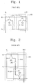
- a 2T-2C type DRAM unit cell is now described below with reference to FIG. 1 and FIG. 2.
- a conventional 2T-2C type DRAM unit cell 100 is illustrated.
- a first cell transistor 101 has a gate coupled to a wordline WL, a drain coupled to a bitline BL, and a source coupled to one electrode of a first cell capacitor 102.
- the other electrode of the first cell capacitor 102 is coupled to a plate line PL.
- a second cell transistor 103 has a gate coupled to the wordline WL, a drain coupled to a complementary bitline BLB, and a source coupled to one electrode of a second cell capacitor 104.
- the other electrode of the second cell capacitor 104 is coupled to the plate line PL.
- the first cell transistor 101 and the first cell capacitor 102 constitute a memory cell CELL
- the second cell transistor 103 and the second cell capacitor 104 constitute a complementary memory cell CELLB. Accordingly, data stored in the first cell capacitor 102 is complementary with data stored in the second cell capacitor 104.
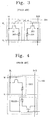
- FIG. 2 another conventional 2T-2C type DRAM unit cell 200 is illustrated.
- a first cell transistor 201 and a first cell capacitor 202 and a second cell transistor 203 and a second cell capacitor 204 are reflected with respect to a plate PL.
- the DRAM cells 100 and 200 are copied or reflected in the row (or wordline) direction and/or the column (or bitline) direction to be disposed in a memory cell block.
- Ferroelectric random access memory may be variously configured with memory cells.
- FIG. 3 and FIG. 4 illustrate 2T-2C type FRAM cells 300 and 400 which are similar to the 2T-2C type DRAM cells 100 and 200, respectively.
- a first ferroelectric capacitor 302 coupled to a first cell transistor 301 and a second ferroelectric capacitor 304 coupled to a second cell transistor 303 are magnetized with opposite polarity.
- the FRAM cell connection structures of FIG. 1 and FIG. 2 are identical with those of FIG. 3 and FIG. 4, respectively.
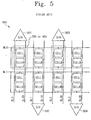
- FIG. 5 illustrates a memory array 500 including the same unit cells as shown in FIG. 2 or FIG. 4.
- First and third bitline/complementary bitline couples BL0/BL0B and BL2/BL2B are connected to the sense amplifiers 501 and 503 over the memory cell array, respectively.
- Second and fourth bitline/complementary bitline couples BL1/BL1B and BL3/BL3B are connected to the sense amplifiers 502 and 504 disposed under the memory cell array, respectively.
- the technical problem to be solved by the present invention is to provide for a memory device having memory and complimentary memory cells and to provide a corresponding method of reading a respective memory cell, which device and method are suited to reach high integration densities by reducing chip size and to need a fairly low power consumption.
- a memory device includes a memory cell array block, a first sense amplifier, a second sense amplifier, a first switch, and a second switch.
- a memory cell array block has pairs of memory cells each of which are composed of a memory cell and a complementary memory cell and are disposed at intersections of rows and columns.
- first and second memory cells and first and second complementary memory cells are connected to a first wordline arranged in the row direction, third and fourth memory cells and third and fourth complementary memory cells are connected to a second wordline, the first and third memory cells are adjacently disposed between the first and second wordlines, the second and fourth memory cells are adjacently disposed therebetween, the first and second complementary memory cells are adjacently disposed therebetween, and the third and fourth complementary memory cells are adjacently disposed therebetween.
- the first sense amplifier is disposed over the memory cell array block, and the second sense amplifier is disposed under the memory cell array block.
- the first switch connects bitlines coupled to the first memory cell and the first complementary memory cell with the first sense amplifier and connects bitlines coupled to the second memory cell and the second complementary memory cell with the second sense amplifier.
- the second switch connects bitlines coupled to the third memory cell and the third complementary memory cell with the first sense amplifier and connects bitlines coupled to the fourth memory cell and the fourth complementary memory cell with the second sense amplifier.
- the pair of the memory cells are further arranged such that the first and second memory cells and the first and second complementary memory cells are interleaved and the third and fourth memory cells and the third and fourth complementary memory cells are interleaved.
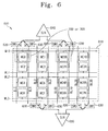
- a memory device 600 includes a memory cell array block 610, a first switch 620, a second switch 630, a first sense amplifier (S/A) 640, and a second sense amplifier (S/A) 650.
- the memory cells MCi and the complementary memory cells MCiB coupled to the first and second wordlines WL0 and WL1 operate the same as the memory cells MCi and the complementary memory cells MCiB coupled to the third and fourth wordlines WL2 and WL3. Therefore, only the memory cells MCi and the complementary memory cells MCiB coupled to the first and second wordlines WL0 and WL1 will be representatively explained in detail.
- memory cells MCi and the complementary memory cells MCiB for example, memory cells MC0 and MC0B constitute one unit memory cell (100 of FIG. 1 or 300 of FIG. 3).
- the first and second memory cells and complementary memory cells MC0, MC1, MC0B, and MC1B are coupled to the first wordline WL0.
- the third and fourth memory cells and complementary memory cells MC2, MC3, MC2B, and MC3B are coupled to the second wordline WL1.
- the first memory cell MC0 and the third memory cell MC2, the second memory cell MC1 and the fourth memory cell MC3, the first complementary memory cell MC0B and the third complementary memory cell MC2B, and the second complementary memory cell MC1B and the fourth complementary memory cell MC3B are adjacently disposed between the first wordline WL0 and the second wordline WL1, respectively.
- the first memory cell MC0 is coupled to the first bitline BL0, and the third memory cell MC2 is coupled to the second bitline BL1.
- the second memory cell MC1 is coupled to the third bitline BL2, and the fourth memory cell MC3 is coupled to the fourth bitline BL3.
- the first complementary memory cell MC0B is coupled to the first complementary bitline BL0B, and the third complementary memory cell MC2B is coupled to the second complementary bitline BL1 B.
- the second complementary memory cell MC1 B is coupled to the third complementary bitline BL2B, and the fourth complementary memory cell MC3B is coupled to the fourth complementary bitline BL3B.
- the first sense amplifier 640 is disposed over the memory cell array block 610.
- the first sense amplifier 640 is connected to the first bitline BL0 and the first complementary bitline BL0B through the first switch 620 and is coupled to the second bitline BL1 and the second complementary bitline BL1B through the second switch 630.
- the second sense amplifier 650 is disposed under the memory cell array block 610.
- the second sense amplifier 650 is connected to the third bitline BL2 and the third complementary bitline BL2B through the first switch 620 and is connected to the fourth bitline BL3 and the fourth complementary bitline BL3B through the second switch 630.
- the first switch 620 When the first switch 620 is switched on, the first bitline BL0 and the first complementary bitline BL0B are connected to the first sense amplifier 640 and the third bitline BL2 and the third complementary bitline BL2B are connected to the second amplifier 650.
- the second switch 630 When the second switch 630 is switched on, the second bitline BL1 and the second complementary bitline BL1B are connected to the first sense amplifier 640 and the fourth bitline BL3 and the fourth complementary bitline BL3B are connected to the second sense amplifier 650.
- the reading operation of the memory device 600 is now explained in detail.
- the first wordline WL0 is enabled and the first switch 620 is switched on
- data of the first memory cell MC0 and data of the first complementary memory cell MC0B are transmitted to the first sense amplifier 640 to be sensed and amplified
- data of the second memory cell MC1 and data of the second complementary memory cell MC1B are transmitted to the second sense amplifier 650 to be sensed and amplified.
- the second bitline BL1 and the second complementary bitline BL1B are not connected to the first sense amplifier 640 to be set to a ground voltage (VSS) level, and fourth bitline BL3 and the fourth complementary bitline BL3B are not connected to the second sense amplifier 650 to be set to the ground voltage (VSS) level.
- a pair of a memory cells CELL and a complementary memory cell CELLB may comprise one unit memory cell.
- the one unit memory cell is selectively connected to the sense amplifiers 640 and 650 through the pair of the memory cell CELL and the complementary memory cell CELLB.
- the number of the sense amplifiers 640 and 650 corresponds to a half of the number of the sense amplifiers 501, 502, 503, and 504 arranged in the conventional memory device 500 shown in FIG. 5. Accordingly, the pattern density is decreased to easily perform a layout and an integration process. Further, the number of sense amplifiers operating at the same time decreases by half to reduce the power consumption.
- the first and second memory cells are interleaved with the first and second complementary memory cells as shown in FIG. 6.
- moving from BL0 towards BL3B one encounters first memory cell, then the second memory cell, then the first complementary memory cell and the second complementary cell.
- the first pair of memory cells, or the first unit memory cell is interleaved with the second pair of memory cells, or the second unit memory cell.
- a similar arrangement occurs for the third and fourth unit memory cells.
Landscapes
- Engineering & Computer Science (AREA)
- Microelectronics & Electronic Packaging (AREA)
- Computer Hardware Design (AREA)
- Dram (AREA)
- Semiconductor Memories (AREA)
Abstract
Description
- The present invention relates to a memory device in which memory cells having complementary data are arranged, and to a corresponding method of reading memory cells.
- Typically, 1T-1C (one transistor and one capacitor) type DRAMs have been used. Instead of the 1T-1C type DRAMs, 2T-2C (two transistors and two capacitors) type DRAMs may be used. The 2T-2C type DRAM has the disadvantage that its memory cell area is large, while having the advantage that, its memory cell sensing margin is almost double the memory cell sensing margin of the IT-1C type DRAM cell because complementary data is stored in one DRAM cell, and a reference voltage for a bitline sense amplifier is unnecessary.
- A 2T-2C type DRAM unit cell is now described below with reference to FIG. 1 and FIG. 2.
- Referring to FIG. 1, a conventional 2T-2C type
DRAM unit cell 100 is illustrated. Afirst cell transistor 101 has a gate coupled to a wordline WL, a drain coupled to a bitline BL, and a source coupled to one electrode of afirst cell capacitor 102. The other electrode of thefirst cell capacitor 102 is coupled to a plate line PL. Asecond cell transistor 103 has a gate coupled to the wordline WL, a drain coupled to a complementary bitline BLB, and a source coupled to one electrode of asecond cell capacitor 104. The other electrode of thesecond cell capacitor 104 is coupled to the plate line PL. Thefirst cell transistor 101 and thefirst cell capacitor 102 constitute a memory cell CELL, and thesecond cell transistor 103 and thesecond cell capacitor 104 constitute a complementary memory cell CELLB. Accordingly, data stored in thefirst cell capacitor 102 is complementary with data stored in thesecond cell capacitor 104. - Referring to FIG. 2, another conventional 2T-2C type
DRAM unit cell 200 is illustrated. Afirst cell transistor 201 and a first cell capacitor 202 and asecond cell transistor 203 and asecond cell capacitor 204 are reflected with respect to a plate PL. - The
DRAM cells - Ferroelectric random access memory (FRAM) may be variously configured with memory cells. FIG. 3 and FIG. 4 illustrate 2T-2C
type FRAM cells type DRAM cells ferroelectric capacitor 302 coupled to afirst cell transistor 301 and a secondferroelectric capacitor 304 coupled to asecond cell transistor 303 are magnetized with opposite polarity. The FRAM cell connection structures of FIG. 1 and FIG. 2 are identical with those of FIG. 3 and FIG. 4, respectively. - FIG. 5 illustrates a
memory array 500 including the same unit cells as shown in FIG. 2 or FIG. 4. First to eighth memory cells coupled to a first wordline WL0 and ninth to sixteenth memory cells coupled to a second wordline WL1 are connected to sense amplifiers (S/A) 501, 502, 503, and 504 through bitlines BLi (i=0, 1, 2, 3) and complementary bitline BLiB (i=0, 1, 2, 3). First and third bitline/complementary bitline couples BL0/BL0B and BL2/BL2B are connected to thesense amplifiers sense amplifiers - As the memory capacity increase, arranged memory cells as well as sense amplifiers increase in number. Thus a layout area occupied by the sense amplifies increases and the sense amplifiers are densely populated, which makes it difficult to perform an integration process. In addition, power consumption increases along with increase in number of the arranged sense amplifiers because they operate at the same time. Accordingly, there is a demand for a memory device having a memory block arrangement which can reduce chip size and power consumption.
- The technical problem to be solved by the present invention is to provide for a memory device having memory and complimentary memory cells and to provide a corresponding method of reading a respective memory cell, which device and method are suited to reach high integration densities by reducing chip size and to need a fairly low power consumption.
- This problem is solved by the present invention providing a memory device according to
claim 1 and a cell reading method according to claim 5. Further preferred embodiments of the invention are given by the subclaims. The contents of all claims are fully incorporated in the present description by reference to avoid unnecessary text repetitions. - In accordance with an embodiment of the invention, a memory device includes a memory cell array block, a first sense amplifier, a second sense amplifier, a first switch, and a second switch. A memory cell array block has pairs of memory cells each of which are composed of a memory cell and a complementary memory cell and are disposed at intersections of rows and columns. In the memory cell array block, first and second memory cells and first and second complementary memory cells are connected to a first wordline arranged in the row direction, third and fourth memory cells and third and fourth complementary memory cells are connected to a second wordline, the first and third memory cells are adjacently disposed between the first and second wordlines, the second and fourth memory cells are adjacently disposed therebetween, the first and second complementary memory cells are adjacently disposed therebetween, and the third and fourth complementary memory cells are adjacently disposed therebetween. The first sense amplifier is disposed over the memory cell array block, and the second sense amplifier is disposed under the memory cell array block. The first switch connects bitlines coupled to the first memory cell and the first complementary memory cell with the first sense amplifier and connects bitlines coupled to the second memory cell and the second complementary memory cell with the second sense amplifier. The second switch connects bitlines coupled to the third memory cell and the third complementary memory cell with the first sense amplifier and connects bitlines coupled to the fourth memory cell and the fourth complementary memory cell with the second sense amplifier.
- Preferably, the pair of the memory cells are further arranged such that the first and second memory cells and the first and second complementary memory cells are interleaved and the third and fourth memory cells and the third and fourth complementary memory cells are interleaved.
- Embodiments of the invention, as described in detail below, and the conventional embodiments described above are illustrated in the drawings, in which:
- FIG. 1 shows a circuit diagram of a conventional 2T-2C type DRAM cell,
- FIG. 2 shows a circuit diagram of another conventional 2T-2C type DRAM cell,
- FIG. 3 shows a circuit diagram of a conventional 2T-2C type FRAM cell,
- FIG. 4 shows a circuit diagram of another conventional 2T-2C type FRAM cell,
- FIG. 5 shows a block diagram of a conventional memory block having the same memory cells as shown in FIG. 2 or FIG. 4, and
- FIG. 6 shows a block diagram of a memory device having a memory cell arrangement according to the present invention.
-
- Referring to FIG. 6, a
memory device 600 includes a memorycell array block 610, afirst switch 620, asecond switch 630, a first sense amplifier (S/A) 640, and a second sense amplifier (S/A) 650. In the memorycell array block 610, a plurality of memory cells Mci (i=0,...,7) and a plurality of complementary memory cells MciB (i=1,...,7) are disposed at intersections of rows and columns. First to fourth wordlines WL0, WL1, WL2, and WL3 are disposed in the row direction, and first to fourth bitlines BLi (i=0, 1, 2, 3) and first to fourth complementary bitlines BLiB (i=0, 1, 2, 3) are disposed in the column direction. The memory cells MCi and the complementary memory cells MCiB coupled to the first and second wordlines WL0 and WL1 operate the same as the memory cells MCi and the complementary memory cells MCiB coupled to the third and fourth wordlines WL2 and WL3. Therefore, only the memory cells MCi and the complementary memory cells MCiB coupled to the first and second wordlines WL0 and WL1 will be representatively explained in detail. Of the memory cells MCi and the complementary memory cells MCiB, for example, memory cells MC0 and MC0B constitute one unit memory cell (100 of FIG. 1 or 300 of FIG. 3). - The first and second memory cells and complementary memory cells MC0, MC1, MC0B, and MC1B are coupled to the first wordline WL0. The third and fourth memory cells and complementary memory cells MC2, MC3, MC2B, and MC3B are coupled to the second wordline WL1. The first memory cell MC0 and the third memory cell MC2, the second memory cell MC1 and the fourth memory cell MC3, the first complementary memory cell MC0B and the third complementary memory cell MC2B, and the second complementary memory cell MC1B and the fourth complementary memory cell MC3B are adjacently disposed between the first wordline WL0 and the second wordline WL1, respectively. The first memory cell MC0 is coupled to the first bitline BL0, and the third memory cell MC2 is coupled to the second bitline BL1. The second memory cell MC1 is coupled to the third bitline BL2, and the fourth memory cell MC3 is coupled to the fourth bitline BL3. The first complementary memory cell MC0B is coupled to the first complementary bitline BL0B, and the third complementary memory cell MC2B is coupled to the second complementary bitline BL1 B. The second complementary memory cell MC1 B is coupled to the third complementary bitline BL2B, and the fourth complementary memory cell MC3B is coupled to the fourth complementary bitline BL3B.
- The
first sense amplifier 640 is disposed over the memorycell array block 610. Thefirst sense amplifier 640 is connected to the first bitline BL0 and the first complementary bitline BL0B through thefirst switch 620 and is coupled to the second bitline BL1 and the second complementary bitline BL1B through thesecond switch 630. Thesecond sense amplifier 650 is disposed under the memorycell array block 610. Thesecond sense amplifier 650 is connected to the third bitline BL2 and the third complementary bitline BL2B through thefirst switch 620 and is connected to the fourth bitline BL3 and the fourth complementary bitline BL3B through thesecond switch 630. When thefirst switch 620 is switched on, the first bitline BL0 and the first complementary bitline BL0B are connected to thefirst sense amplifier 640 and the third bitline BL2 and the third complementary bitline BL2B are connected to thesecond amplifier 650. When thesecond switch 630 is switched on, the second bitline BL1 and the second complementary bitline BL1B are connected to thefirst sense amplifier 640 and the fourth bitline BL3 and the fourth complementary bitline BL3B are connected to thesecond sense amplifier 650. - The reading operation of the
memory device 600 is now explained in detail. When the first wordline WL0 is enabled and thefirst switch 620 is switched on, data of the first memory cell MC0 and data of the first complementary memory cell MC0B are transmitted to thefirst sense amplifier 640 to be sensed and amplified, and data of the second memory cell MC1 and data of the second complementary memory cell MC1B are transmitted to thesecond sense amplifier 650 to be sensed and amplified. At this time, since thesecond switch 630 is switched off, the second bitline BL1 and the second complementary bitline BL1B are not connected to thefirst sense amplifier 640 to be set to a ground voltage (VSS) level, and fourth bitline BL3 and the fourth complementary bitline BL3B are not connected to thesecond sense amplifier 650 to be set to the ground voltage (VSS) level. - A pair of a memory cells CELL and a complementary memory cell CELLB, may comprise one unit memory cell. The one unit memory cell is selectively connected to the
sense amplifiers sense amplifiers sense amplifiers conventional memory device 500 shown in FIG. 5. Accordingly, the pattern density is decreased to easily perform a layout and an integration process. Further, the number of sense amplifiers operating at the same time decreases by half to reduce the power consumption. - The first and second memory cells are interleaved with the first and second complementary memory cells as shown in FIG. 6. In that example, moving from BL0 towards BL3B one encounters first memory cell, then the second memory cell, then the first complementary memory cell and the second complementary cell. In this fashion, the first pair of memory cells, or the first unit memory cell, is interleaved with the second pair of memory cells, or the second unit memory cell. A similar arrangement occurs for the third and fourth unit memory cells.
- While the present invention has been described with respect to the particular embodiments, it will be apparent to a person skilled in the art that various modifications and substitutions may be made without departing from the scope of the invention as defined in the following claims.
Claims (6)
- A memory device, comprising:an array of unit memory cells, each unit memory cell comprising a memory cell (MC0, ..., MC7) and a complementary memory cell (MC0B, ..., MC7B);bitlines (BL0, ..., BL3) arranged such that a first and a third unit memory cells are connected to a first bitline, and a second and a fourth unit memory cells are connected to a second bitline, wherein the complementary cell of each unit memory cell is connected to a complementary bitline (BL0B, ..., BL3B) to the bitline connected to the memory cell;sense amplifiers (640, 650) arranged adjacent the array; andswitches (620, 630) arranged such that the first and third bitlines (BL0, BL2) are controlled by a first switch (620) and the second and fourth bitlines (BL1, BL3) are controlled by a second switch (630) to selectively connect the bitlines to the sense amplifiers.
- The memory device of claim 1, the first unit memory cell and the second memory cell being arranged in an interleaved fashion, and the third unit memory cell and the fourth unit memory cell being interleaved.
- A memory device of claim 1 or 2, characterized in that:the memory cell array is arranged in one or more blocks comprising the unit memory cells, each cell being disposed at intersections of rows and columns, in which the first and second memory cells and the first and second complementary memory cells are connected to a first wordline (WLO) arranged in the row direction, the third and fourth memory cells and third and fourth complementary memory cells are connected to a second wordline (WL1), the first and third memory cells are adjacently disposed between the first and second wordlines, the second and fourth memory cells are adjacently disposed therebetween, the first and third complementary memory cells are adjacently disposed therebetween, and the second and fourth complementary memory cells are adjacently disposed therebetween;a first one of the sense amplifiers being disposed over the memory cell array block;a second one of the sense amplifiers being disposed under the memory cell array block;the first switch (620) connecting the bitlines (BL0, BL0B) coupled to the first memory cell and the first complementary memory cell with the first sense amplifier (640) and connecting the bitlines (BL2, BL2B) coupled to the second memory cell and the second complementary memory cell with the second sense amplifier (650); andthe second switch (630) connecting the bitlines (BL1, BL1B) coupled to the third memory cell and the third complementary memory cell with the first sense amplifier and connecting the bitlines (BL3, BL3B) coupled to the fourth memory cell and the fourth complementary memory cell with the second sense amplifier.
- The memory device of claim 3, characterized in that when the first wordline is enabled to connect the first memory cell and the first complementary memory cell with the first sense amplifier and connect the second memory cell and the second complementary memory cell with the second sense amplifier, the third and fourth memory cells and third and fourth complementary memory cells, which are coupled to the second wordline, are set to a ground voltage level.
- A method of reading a memory cell, the method comprising:enabling a first wordline (WL0);turning on a first switch (620) connected to the first wordline;transmitting data from a first memory cell (MC0) to a first sense amplifier (640) using a first bitline (BL0); andtransmitting data from a second memory cell (MC1) to a second sense amplifier (650) using a third bitline (BL2).
- The method of claim 5, the method further comprising setting a second bitline (BL1) and a fourth bitline (BL3) to a ground voltage.
Applications Claiming Priority (2)
| Application Number | Priority Date | Filing Date | Title |
|---|---|---|---|
| KR10-2002-0054169A KR100456598B1 (en) | 2002-09-09 | 2002-09-09 | Memory device arranged memory cells having complementary data |
| KR2002054169 | 2002-09-09 |
Publications (2)
| Publication Number | Publication Date |
|---|---|
| EP1398787A1 true EP1398787A1 (en) | 2004-03-17 |
| EP1398787B1 EP1398787B1 (en) | 2006-03-01 |
Family
ID=36129266
Family Applications (1)
| Application Number | Title | Priority Date | Filing Date |
|---|---|---|---|
| EP03018821A Expired - Lifetime EP1398787B1 (en) | 2002-09-09 | 2003-08-19 | Memory device having memory cell units each composed of a memory and complementary memory cell and reading method |
Country Status (5)
| Country | Link |
|---|---|
| US (1) | US6961271B2 (en) |
| EP (1) | EP1398787B1 (en) |
| JP (1) | JP2004103213A (en) |
| KR (1) | KR100456598B1 (en) |
| DE (1) | DE60303721T2 (en) |
Families Citing this family (23)
| Publication number | Priority date | Publication date | Assignee | Title |
|---|---|---|---|---|
| US20030036698A1 (en) * | 2001-08-16 | 2003-02-20 | Robert Kohler | Interventional diagnostic catheter and a method for using a catheter to access artificial cardiac shunts |
| DE102006058865B4 (en) * | 2005-12-07 | 2010-06-10 | Samsung Electronics Co., Ltd., Suwon | Semiconductor memory device and method for writing data |
| US20090257263A1 (en) * | 2008-04-15 | 2009-10-15 | Vns Portfolio Llc | Method and Apparatus for Computer Memory |
| US8130559B1 (en) | 2008-08-06 | 2012-03-06 | Altera Corporation | MEMS switching device and conductive bridge device based circuits |
| US8477526B2 (en) * | 2011-04-27 | 2013-07-02 | Robert Newton Rountree | Low noise memory array |
| ITTO20120682A1 (en) * | 2012-07-31 | 2014-02-01 | St Microelectronics Pvt Ltd | NON-VOLATILE MEMORY DEVICE WITH GROUPED CELLS |
| KR102188490B1 (en) | 2016-08-31 | 2020-12-09 | 마이크론 테크놀로지, 인크. | Apparatus and method for accessing ferroelectric memory including ferroelectric memory |
| KR102171724B1 (en) | 2016-08-31 | 2020-10-30 | 마이크론 테크놀로지, 인크 | Memory cells and memory arrays |
| CN109155312B (en) | 2016-08-31 | 2023-05-02 | 美光科技公司 | Memory cells and memory arrays |
| US10115438B2 (en) | 2016-08-31 | 2018-10-30 | Micron Technology, Inc. | Sense amplifier constructions |
| WO2018044456A1 (en) | 2016-08-31 | 2018-03-08 | Micron Technology, Inc. | Memory cells and memory arrays |
| EP3507804A4 (en) | 2016-08-31 | 2020-07-15 | Micron Technology, INC. | FERROELECTRIC STORAGE CELLS |
| US10276230B2 (en) | 2016-08-31 | 2019-04-30 | Micron Technology, Inc. | Memory arrays |
| KR102208380B1 (en) | 2016-08-31 | 2021-01-28 | 마이크론 테크놀로지, 인크 | Memory cells and memory arrays |
| EP3507805B1 (en) | 2016-08-31 | 2025-10-01 | Micron Technology, Inc. | Apparatuses and methods including ferroelectric memory and for operating ferroelectric memory |
| US10355002B2 (en) | 2016-08-31 | 2019-07-16 | Micron Technology, Inc. | Memory cells, methods of forming an array of two transistor-one capacitor memory cells, and methods used in fabricating integrated circuitry |
| WO2018044510A1 (en) | 2016-08-31 | 2018-03-08 | Micron Technology, Inc. | Apparatuses and methods including two transistor-one capacitor memory and for accessing same |
| WO2018132250A1 (en) | 2017-01-12 | 2018-07-19 | Micron Technology, Inc. | Memory cells, arrays of two transistor-one capacitor memory cells, methods of forming an array of two transistor-one capacitor memory cells, and methods used in fabricating integrated circuitry |
| US10867675B2 (en) * | 2017-07-13 | 2020-12-15 | Micron Technology, Inc. | Apparatuses and methods for memory including ferroelectric memory cells and dielectric memory cells |
| EP3676835A4 (en) | 2017-08-29 | 2020-08-19 | Micron Technology, Inc. | MEMORY CIRCUIT |
| US10347322B1 (en) * | 2018-02-20 | 2019-07-09 | Micron Technology, Inc. | Apparatuses having memory strings compared to one another through a sense amplifier |
| CN114155896B (en) * | 2020-09-04 | 2024-03-29 | 长鑫存储技术有限公司 | Semiconductor device with a semiconductor device having a plurality of semiconductor chips |
| DE102020211842B4 (en) * | 2020-09-22 | 2026-02-05 | Infineon Technologies Ag | Storage devices and methods for operating them |
Citations (4)
| Publication number | Priority date | Publication date | Assignee | Title |
|---|---|---|---|---|
| US4599704A (en) * | 1984-01-03 | 1986-07-08 | Raytheon Company | Read only memory circuit |
| US5218566A (en) * | 1991-08-15 | 1993-06-08 | National Semiconductor Corporation | Dynamic adjusting reference voltage for ferroelectric circuits |
| JPH09330596A (en) * | 1996-06-10 | 1997-12-22 | Hitachi Ltd | Non-volatile storage device |
| EP1081714A1 (en) * | 1999-08-31 | 2001-03-07 | Fujitsu Limited | DRAM for storing data in pairs of cells |
Family Cites Families (10)
| Publication number | Priority date | Publication date | Assignee | Title |
|---|---|---|---|---|
| DE3887924T3 (en) * | 1987-06-02 | 1999-08-12 | National Semiconductor Corp., Santa Clara, Calif. | Non-volatile memory arrangement with a capacitive ferroelectric memory element. |
| JPH02231759A (en) * | 1989-03-03 | 1990-09-13 | Mitsubishi Electric Corp | Semiconductor device |
| JPH09147576A (en) * | 1995-11-24 | 1997-06-06 | Sony Corp | Ferroelectric memory device |
| US5864496A (en) * | 1997-09-29 | 1999-01-26 | Siemens Aktiengesellschaft | High density semiconductor memory having diagonal bit lines and dual word lines |
| JPH11306751A (en) * | 1998-04-22 | 1999-11-05 | Toshiba Corp | Semiconductor storage device |
| KR100555456B1 (en) * | 1998-11-11 | 2006-05-16 | 삼성전자주식회사 | Data transmission circuit and its data transmission method |
| US6272054B1 (en) * | 2000-10-31 | 2001-08-07 | International Business Machines Corporation | Twin-cell memory architecture with shielded bitlines for embedded memory applications |
| JP2002216471A (en) * | 2001-01-17 | 2002-08-02 | Mitsubishi Electric Corp | Semiconductor storage device |
| JP2002237196A (en) * | 2001-02-13 | 2002-08-23 | Nec Corp | Memory and its operating method |
| JP4392680B2 (en) * | 2002-09-05 | 2010-01-06 | エルピーダメモリ株式会社 | Semiconductor memory device |
-
2002
- 2002-09-09 KR KR10-2002-0054169A patent/KR100456598B1/en not_active Expired - Fee Related
-
2003
- 2003-07-14 US US10/620,022 patent/US6961271B2/en not_active Expired - Fee Related
- 2003-08-05 JP JP2003286575A patent/JP2004103213A/en active Pending
- 2003-08-19 DE DE60303721T patent/DE60303721T2/en not_active Expired - Lifetime
- 2003-08-19 EP EP03018821A patent/EP1398787B1/en not_active Expired - Lifetime
Patent Citations (4)
| Publication number | Priority date | Publication date | Assignee | Title |
|---|---|---|---|---|
| US4599704A (en) * | 1984-01-03 | 1986-07-08 | Raytheon Company | Read only memory circuit |
| US5218566A (en) * | 1991-08-15 | 1993-06-08 | National Semiconductor Corporation | Dynamic adjusting reference voltage for ferroelectric circuits |
| JPH09330596A (en) * | 1996-06-10 | 1997-12-22 | Hitachi Ltd | Non-volatile storage device |
| EP1081714A1 (en) * | 1999-08-31 | 2001-03-07 | Fujitsu Limited | DRAM for storing data in pairs of cells |
Non-Patent Citations (1)
| Title |
|---|
| PATENT ABSTRACTS OF JAPAN vol. 1998, no. 04 31 March 1998 (1998-03-31) * |
Also Published As
| Publication number | Publication date |
|---|---|
| DE60303721T2 (en) | 2006-09-21 |
| KR20040022566A (en) | 2004-03-16 |
| US20040047197A1 (en) | 2004-03-11 |
| KR100456598B1 (en) | 2004-11-09 |
| EP1398787B1 (en) | 2006-03-01 |
| DE60303721D1 (en) | 2006-04-27 |
| JP2004103213A (en) | 2004-04-02 |
| US6961271B2 (en) | 2005-11-01 |
Similar Documents
| Publication | Publication Date | Title |
|---|---|---|
| EP1398787B1 (en) | Memory device having memory cell units each composed of a memory and complementary memory cell and reading method | |
| US6538914B1 (en) | Ferroelectric memory with bit-plate parallel architecture and operating method thereof | |
| CN115171750A (en) | Memory, access method thereof and electronic equipment | |
| US6297985B1 (en) | Cell block structure of nonvolatile ferroelectric memory | |
| KR100709538B1 (en) | Semiconductor memory | |
| JPH08167290A (en) | Semiconductor memory device | |
| CN105261391B (en) | A kind of SRAM storage arrays | |
| CN212230079U (en) | Ferroelectric memory storage array structure and ferroelectric memory | |
| JP3913451B2 (en) | Semiconductor memory device | |
| JPH11238388A (en) | Semiconductor storage device | |
| KR100316241B1 (en) | Nonvolatile Ferroelectric Memory | |
| US20030043667A1 (en) | Multiple word-line accessing and accessor | |
| JP2004030905A (en) | Method and device for memory detection | |
| US6504747B2 (en) | Integrated memory with plate line segments | |
| KR100447222B1 (en) | Ferroelectric memory and method for driving the same | |
| JP3817409B2 (en) | Integrated memory | |
| KR100621769B1 (en) | Bitline Arrangement Structure in Semiconductor Memory Device | |
| KR100449953B1 (en) | Cell array of FeRAM | |
| KR101362726B1 (en) | Memory apparatus and driving method thereof | |
| KR100568861B1 (en) | Ferroelectric memory device with reference voltage generator | |
| US7511983B2 (en) | Memory device with hierarchy bit line | |
| KR20010102574A (en) | Integrated memory with memory cells and reference cells and operating method for a memory of this type | |
| US7099178B2 (en) | Ferromagnetic random access memory | |
| KR101319529B1 (en) | Memory apparatus having sense amplifier and driving method thereof | |
| KR100255515B1 (en) | Ferroelectric memory device |
Legal Events
| Date | Code | Title | Description |
|---|---|---|---|
| PUAI | Public reference made under article 153(3) epc to a published international application that has entered the european phase |
Free format text: ORIGINAL CODE: 0009012 |
|
| AK | Designated contracting states |
Kind code of ref document: A1 Designated state(s): AT BE BG CH CY CZ DE DK EE ES FI FR GB GR HU IE IT LI LU MC NL PT RO SE SI SK TR |
|
| AX | Request for extension of the european patent |
Extension state: AL LT LV MK |
|
| 17P | Request for examination filed |
Effective date: 20040421 |
|
| RIN1 | Information on inventor provided before grant (corrected) |
Inventor name: CHOI, MUN KYU Inventor name: JEON, BYUNG GIL Inventor name: KIM, KI NAM |
|
| 17Q | First examination report despatched |
Effective date: 20040525 |
|
| AKX | Designation fees paid |
Designated state(s): DE FR GB |
|
| GRAP | Despatch of communication of intention to grant a patent |
Free format text: ORIGINAL CODE: EPIDOSNIGR1 |
|
| GRAS | Grant fee paid |
Free format text: ORIGINAL CODE: EPIDOSNIGR3 |
|
| GRAA | (expected) grant |
Free format text: ORIGINAL CODE: 0009210 |
|
| AK | Designated contracting states |
Kind code of ref document: B1 Designated state(s): DE FR GB |
|
| REG | Reference to a national code |
Ref country code: GB Ref legal event code: FG4D |
|
| REF | Corresponds to: |
Ref document number: 60303721 Country of ref document: DE Date of ref document: 20060427 Kind code of ref document: P |
|
| ET | Fr: translation filed | ||
| PLBE | No opposition filed within time limit |
Free format text: ORIGINAL CODE: 0009261 |
|
| STAA | Information on the status of an ep patent application or granted ep patent |
Free format text: STATUS: NO OPPOSITION FILED WITHIN TIME LIMIT |
|
| 26N | No opposition filed |
Effective date: 20061204 |
|
| REG | Reference to a national code |
Ref country code: FR Ref legal event code: PLFP Year of fee payment: 14 |
|
| REG | Reference to a national code |
Ref country code: FR Ref legal event code: PLFP Year of fee payment: 15 |
|
| REG | Reference to a national code |
Ref country code: FR Ref legal event code: PLFP Year of fee payment: 16 |
|
| PGFP | Annual fee paid to national office [announced via postgrant information from national office to epo] |
Ref country code: FR Payment date: 20200721 Year of fee payment: 18 Ref country code: GB Payment date: 20200722 Year of fee payment: 18 Ref country code: DE Payment date: 20200721 Year of fee payment: 18 |
|
| REG | Reference to a national code |
Ref country code: DE Ref legal event code: R119 Ref document number: 60303721 Country of ref document: DE |
|
| GBPC | Gb: european patent ceased through non-payment of renewal fee |
Effective date: 20210819 |
|
| PG25 | Lapsed in a contracting state [announced via postgrant information from national office to epo] |
Ref country code: GB Free format text: LAPSE BECAUSE OF NON-PAYMENT OF DUE FEES Effective date: 20210819 Ref country code: FR Free format text: LAPSE BECAUSE OF NON-PAYMENT OF DUE FEES Effective date: 20210831 Ref country code: DE Free format text: LAPSE BECAUSE OF NON-PAYMENT OF DUE FEES Effective date: 20220301 |
|
| P01 | Opt-out of the competence of the unified patent court (upc) registered |
Effective date: 20230520 |