EP1396883A2 - Substrate and manufacturing method therefor - Google Patents
Substrate and manufacturing method therefor Download PDFInfo
- Publication number
- EP1396883A2 EP1396883A2 EP03020006A EP03020006A EP1396883A2 EP 1396883 A2 EP1396883 A2 EP 1396883A2 EP 03020006 A EP03020006 A EP 03020006A EP 03020006 A EP03020006 A EP 03020006A EP 1396883 A2 EP1396883 A2 EP 1396883A2
- Authority
- EP
- European Patent Office
- Prior art keywords
- layer
- substrate
- semiconductor layer
- semiconductor
- forming
- Prior art date
- Legal status (The legal status is an assumption and is not a legal conclusion. Google has not performed a legal analysis and makes no representation as to the accuracy of the status listed.)
- Withdrawn
Links
Images




Classifications
-
- H—ELECTRICITY
- H10—SEMICONDUCTOR DEVICES; ELECTRIC SOLID-STATE DEVICES NOT OTHERWISE PROVIDED FOR
- H10P—GENERIC PROCESSES OR APPARATUS FOR THE MANUFACTURE OR TREATMENT OF DEVICES COVERED BY CLASS H10
- H10P90/00—Preparation of wafers not covered by a single main group of this subclass, e.g. wafer reinforcement
- H10P90/19—Preparing inhomogeneous wafers
- H10P90/1904—Preparing vertically inhomogeneous wafers
- H10P90/1906—Preparing SOI wafers
- H10P90/1924—Preparing SOI wafers with separation/delamination along a porous layer
-
- H—ELECTRICITY
- H10—SEMICONDUCTOR DEVICES; ELECTRIC SOLID-STATE DEVICES NOT OTHERWISE PROVIDED FOR
- H10W—GENERIC PACKAGES, INTERCONNECTIONS, CONNECTORS OR OTHER CONSTRUCTIONAL DETAILS OF DEVICES COVERED BY CLASS H10
- H10W10/00—Isolation regions in semiconductor bodies between components of integrated devices
- H10W10/10—Isolation regions comprising dielectric materials
- H10W10/181—Semiconductor-on-insulator [SOI] isolation regions, e.g. buried oxide regions of SOI wafers
Definitions
- the present invention relates to a substrate and manufacturing method therefor and, more particularly, to a substrate having a partial insulating layer inside and a manufacturing method therefor.
- This substrate is referred to as a Semiconductor-On-Insulator substrate or Silicon-On-Insulator substrate.
- the latter substrate is one of Semiconductor-On-Insulator substrates and has a semiconductor layer made of silicon. Both Semiconductor-On-Insulator substrates and Silicon-On-Insulator substrates are called SOI substrates.
- a substrate which has an insulating layer not in the entire region but in a partial region under a semiconductor layer or an Si layer has been proposed.
- a related art is disclosed in Japanese Patent No. 2794702 (semiconductor device manufacturing method).
- a manufacturing method disclosed in Japanese Patent No. 2794702 forms an n + -layer on an n - -silicon substrate serving as the first substrate, forms a thermal oxide film (SiO 2 ) on the n + -layer, and then removes an unnecessary portion of the thermal oxide film. With this operation, the thermal oxide film is partially left on the n + -layer. After that, an epitaxial layer is grown on an exposed portion of the n-layer.
- a polysilicon layer is formed on the partial thermal oxide film.
- the main surface of the first substrate is polished such that the epitaxial and polysilicon layers have the same height.
- the main surface side of the first substrate is bonded to the second substrate, thereby obtaining a final substrate.
- This final substrate has a partial buried insulating layer (thermal oxide film) under a portion constituted by the first substrate.
- a semiconductor device is formed on the portion constituted by the first substrate.
- a portion on which a device is to be formed is the first substrate itself in a final substrate to be manufactured, and the thickness is very large. For this reason, it is difficult for the final substrate to enjoy the advantages of a general SOI substrate. More specifically, a substrate obtained by the manufacturing method disclosed in Japanese Patent No. 2794702 cannot sufficiently exhibit the advantages of an SOI substrate, such as low power consumption, high-speed operation, and the like.
- a device structure i.e., a device structure having a larger size in the direction of depth than a device structure to be formed in a region with a buried insulating layer
- the device structure is so formed as to extend through the first substrate, epitaxial layer, and second substrate.
- a device structure formed to extend through bulk silicon (the first and second substrates) and an epitaxial layer cannot easily obtain high quality.
- an existing device structure, an existing device manufacturing process, existing process parameters, and the like may inevitably be changed.
- the manufacturing method disclosed in Japanese Patent No. 2794702 polishes the first substrate, in which the epitaxial layer and polysilicon layer are combined on the surface, before bonding the first and second substrates.
- the polishing step there is a limit to planarization of the surface of the first substrate by the polishing step. More specifically, if the polishing conditions are set for the epitaxial layer, the planarity of the polysilicon layer becomes poor. On the other hand, if the polishing conditions are set for the polysilicon layer, the planarity of the epitaxial layer becomes poor. Additionally, a level difference may occur between the epitaxial layer and the polysilicon layer.
- the first substrate in which the epitaxial layer and polysilicon layer are combined on the surface has poor surface planarity, poor bonding is likely to occur in bonding the first substrate to the second substrate. This poor bonding interferes with the formation of a high-quality device.
- the present invention has been made on the basis of the above consideration.
- the first to third aspects of the present invention have as their object to, e.g., ensure the advantages of an SOI substrate for a substrate having a partial insulating layer under a semiconductor layer.
- a substrate manufacturing method comprising a step of forming a first substrate which has a separation layer, a first semiconductor layer on the separation layer, a partial insulating layer on the first semiconductor layer, and a second semiconductor layer on the first semiconductor layer exposed in the partial insulating layer and the partial insulating layer, a step of bonding a second substrate to the second semiconductor layer on the first substrate to form a bonded substrate stack, and a step of splitting the bonded substrate stack at the separation layer.
- the method preferably further comprises a step of planarizing the second semiconductor layer of the first substrate before bonding the second substrate to the second semiconductor layer on the first substrate.
- a single-crystal semiconductor layer made of the same material as a material of the first semiconductor layer is preferably grown as a part of the second semiconductor layer on the first semiconductor layer exposed in the insulating layer.
- a single-crystal semiconductor layer made of the same material as a material of the first semiconductor layer is grown as a part of the second semiconductor layer on the first semiconductor layer exposed in the insulating layer, and a polycrystalline semiconductor layer made of the same material as a material of the first semiconductor layer is grown as another part of the second semiconductor layer on the partial insulating layer.
- the step of forming the first substrate preferably includes a step of forming a porous layer serving as the separation layer on a semiconductor substrate by anodization and sequentially forming the first semiconductor layer and partial insulating layer on the porous layer.
- the step of forming the first substrate preferably includes a step of forming the separation layer by implanting ions into a semiconductor substrate.
- At least a surface, to be bonded to the first substrate, of the second substrate preferably comprises an insulator.
- a substrate manufacturing method comprising a step of forming a first substrate which has a first semiconductor layer, a partial insulating layer on the first semiconductor layer, and a second semiconductor layer on the first semiconductor layer exposed in the partial insulating layer and the partial insulating layer, a step of bonding a second substrate to the second semiconductor layer on the first substrate to form a bonded substrate stack, and a step of grinding the first substrate constituting a part of the bonded substrate stack from a back surface of the first substrate to thin the bonded substrate stack.
- a substrate comprising a first insulating layer arranged over a whole region inside the substrate, a second partial insulating layer arranged adjacent to or spaced apart from the first insulating layer, on the first insulating layer, and a semiconductor layer arranged on a surface of the substrate.
- the fourth and fifth aspects of the present invention have as their object to improve the quality of a substrate manufactured through, e.g., a step of bonding two substrates.
- a substrate manufacturing method comprising a step of forming a first substrate which has a first semiconductor layer, a partial insulating layer on the first semiconductor layer, and a second semiconductor layer on the first semiconductor layer exposed in the partial insulating layer and the partial insulating layer, a step of forming a third layer on an entire surface of the second semiconductor layer of the first substrate, and a step of bonding a second substrate to the third layer of the first substrate to form a bonded substrate stack.
- the method preferably further comprises a step of removing a part of the first substrate from the bonded substrate stack such that the first semiconductor layer is exposed.
- the step of forming the first substrate includes a step of forming a separation layer under the first semiconductor layer, and the method further comprises a step of splitting the bonded substrate stack at the separation layer.
- the method preferably further comprises a step of planarizing a surface of the third layer after the step of forming the third layer and before the step of forming the bonded substrate stack.
- the method preferably further comprises a step of planarizing a surface of the second semiconductor layer after the step of forming the first substrate and before the step of forming the third layer.
- a layer having a structure substantially uniform across a surface of the layer is preferably formed as the third layer.
- a polycrystalline semiconductor layer, an amorphous semiconductor layer, or an insulating layer is preferably formed as the third layer.
- the insulating layer is formed as the third layer, it preferably comprises an oxide film and the oxide film is preferably formed by CVD.
- a single-crystal semiconductor layer made of the same material as a material of the first semiconductor layer is preferably grown as a part of the second semiconductor layer on the first semiconductor layer exposed in the insulating layer.
- a single-crystal semiconductor layer made of the same material as a material of the first semiconductor layer is preferably grown as a part of the second semiconductor layer on the first semiconductor layer exposed in the insulating layer, and a polycrystalline semiconductor layer made of the same material as the first semiconductor layer is grown as another part of the second semiconductor layer on the partial insulating layer.
- the step of forming the first substrate preferably includes a step of forming a porous layer serving as the separation layer on a semiconductor substrate by anodization and sequentially forming the first semiconductor layer and partial insulating layer on the porous layer.
- a substrate comprising a first semiconductor layer arranged on a surface of the substrate, a first partial insulating layer arranged under the first semiconductor layer, a second semiconductor layer arranged adjacent to and under the first semiconductor layer in the first partial insulating layer and the first partial insulating layer, and a third layer arranged adjacent to and under the second semiconductor layer.
- the third layer preferably has a lower planarized surface.
- the substrate preferably further comprises a handle substrate arranged adjacent to or under the third layer through a fourth layer.
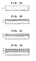
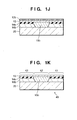
- Figs. 1A to 1K are views for explaining a substrate manufacturing method according to the preferred embodiment of the present invention.
- a single-crystal Si substrate (seed substrate) 11 is prepared, and in the step shown in Fig. 1B, a separation layer 12 is formed on the surface of the single-crystal Si substrate 11.
- the separation layer 12 e.g., a porous layer which can be formed by anodizing the surface of the single-crystal Si substrate 11 is preferably employed.
- This anodization can be performed by, e.g., placing an anode and cathode in an electrolyte solution containing hydrofluoric acid, placing the single-crystal Si substrate 11 between the electrodes, and supplying a current between them.
- the porous layer may comprise two or more layers with different porosities.
- a single-crystal Si layer (first semiconductor layer) 13 is formed on the separation layer 12 by epitaxial growth. Epitaxial growth can form the single-crystal Si layer 13 of good quality.
- a method of implanting ions such as hydrogen ions or the like at a predetermined depth from the surface of the single-crystal Si substrate 11 to form an ion implantation layer serving as the separation layer 12 may be adopted.
- a portion on the surface side from the viewpoint of the separation layer 12 functions as the single-crystal Si layer 13.
- a semiconductor layer made of another material may be formed on the separation layer 12.
- an SiO 2 layer 14 serving as an insulating layer is formed on the single-crystal Si layer 13.
- the SiO 2 layer 14 can be formed by, e.g., thermal oxidation. Thermal oxidation can form an SiO 2 layer of good quality.
- the SiO 2 layer 14 is patterned to form a partial SiO 2 layer 14a.
- a partial SiO 2 layer is defined as an SiO 2 layer which is formed such that the single-crystal Si layer (semiconductor layer) 13 is at least partially exposed.
- the SiO 2 layer 14 can be patterned by, e.g., the following operation. After a mask material is formed on the SiO 2 layer 14, the mask material is patterned by lithography (resist coating, exposure, development, and etching) to form an opening. The SiO 2 layer 14 exposed at the bottom of the opening is then etched by, e.g., reactive ion etching (RIE).
- RIE reactive ion etching
- a step of covering the surface except a region in which the partial SiO 2 layer 14a is to be formed with a mask pattern and forming the partial SiO 2 layer 14a only in an exposed portion may be adopted.
- a single-crystal Si layer (second semiconductor layer) 15 is grown by epitaxial growth on an exposed portion of the single-crystal Si layer 13 in the partial SiO 2 layer 14a.
- a polysilicon layer 16 may be formed on the partial insulating layer 14a.
- the single-crystal Si layer 15 may be grown on the single-crystal Si layer 13 on the condition that the polysilicon layer 16 be not formed on the partial insulating layer 14a.
- the single-crystal Si layer 15 and polysilicon layer 16 are different in growth rate, and a level difference may occur between the single-crystal Si layer 15 and the polysilicon layer 16, as exaggeratedly shown in Fig. 1F.
- Three-dimensional patterns 15a and 16a can be formed on the surfaces of the single-crystal Si layer 15 and polysilicon layer 16, respectively.
- a semiconductor layer made of another material is to be formed instead of the single-crystal Si layer 13.
- a semiconductor layer made of the same material as that of the formed semiconductor layer is preferably formed on the semiconductor layer in the step shown in Fig. 1F.
- a first substrate 10 is so formed as to have the single-crystal Si layer (first semiconductor layer) 13 on the porous layer or ion implantation layer as the separation layer 12, the partial SiO 2 layer (insulating layer) 14a on the single-crystal Si layer 13, and a single-crystal Si layer (second semiconductor layer) 15b on the single-crystal Si layer 13 and a polysilicon layer (second semiconductor layer) 16b on the insulating layer 14a.
- a substrate having a structure shown in Fig. 1G is referred to as the first substrate for the sake of convenience, a substrate having a structure shown in any one of Figs. 1A to 1F may also be referred to as the first substrate.
- a second substrate (handle substrate) 20 is bonded to the surface (a surface in which the single-crystal Si layer 15b and polysilicon layer 16b are exposed) of the first substrate 10 shown in Fig. 1G to form a bonded substrate stack 30.
- An SiO 2 layer may be formed on the surface of the first substrate 10 by, e.g., thermal oxidation, prior to the bonding.
- a single-crystal Si substrate or a substrate obtained by forming an insulating layer such as an SiO 2 layer on the surface can typically be used.
- any other substrate such as an insulating substrate (e.g., a glass substrate) may be adopted as the second substrate 20.
- the bonded substrate stack 30 is split into two substrates by splitting the bonded substrate stack 30 at the separation layer 12.
- This splitting can be performed by, e.g., using a fluid.
- a method of using a fluid a method of forming a jet of a fluid (liquid or gas) and injecting it to the separation layer 12, a method of utilizing the static pressure of a fluid, or the like is preferably used.
- a method of utilizing water as a fluid is referred to as a water jet method.
- the above-mentioned splitting can also be performed by, e.g., annealing the bonded substrate stack 30. Such splitting by annealing is particularly effective in forming an ion implantation layer as the separation layer 12. Additionally, the splitting can be performed by, e.g., inserting a member such as a solid wedge into the separation layer 12.
- a grinding and polishing method in which the back surface (exposed surface) of the bonded substrate stack 30 is ground and polished to leave a single-crystal Si layer with a predetermined thickness on the insulating layer 14a may be adopted.
- the separation layer 12 need not be formed in advance.
- a separation layer 12b left on the single-crystal Si layer 13 of the second substrate 20 is removed using an etchant or the like.
- the single-crystal Si layer 13 can be used as an etching stopper layer.
- the surface of the substrate may be planarized by performing a planarizing step such as a hydrogen annealing step, polishing step, or the like, as needed.
- a semiconductor substrate (partial SOI substrate) 40 as shown in Fig. 1K is obtained.
- the semiconductor substrate 40 shown in Fig. 1K has the thin single-crystal Si layer (first semiconductor layer) 13 on its surface and the partial SiO 2 layer (insulating layer) 14a and single-crystal Si layer 15b under the single-crystal Si layer 13.
- a thin single-crystal Si layer means a layer thinner than a general semiconductor substrate.
- the thickness of the single-crystal Si layer (first semiconductor layer) 13 is preferably, e.g., 10 ⁇ m or less, and more preferably, 5 nm to 2 ⁇ m.
- a region (SOI region) 41 with the partial SiO 2 layer (insulating layer) 14a as a buried insulating layer out of the semiconductor substrate 40 has the same properties as those of an SOI substrate which has a buried insulating film over the whole region.
- a region (non-SOI region) 42 without the partial insulating layer 14a out of the semiconductor substrate 40 i.e., a region which has the single-crystal Si layer 15b under the single-crystal Si layer 13 has substantially the same properties as those of an Si substrate which has an epitaxial Si layer on its surface.
- the single-crystal Si layer 15b is a layer which is formed by epitaxial growth using as the underlying layer the single-crystal Si layer 13 formed by epitaxial growth.
- a defect hardly occurs in the interface between the single-crystal Si layer 13 and the single-crystal Si layer 15b. Accordingly, if the semiconductor substrate 40 is used, a high-quality device can be formed even when a device (e.g., a trench capacitor) having a structure deeper than that of a device to be formed in the SOI region is formed in the non-SOI region.
- a device e.g., a trench capacitor
- the semiconductor substrate 40 which can be manufactured by this embodiment is useful in forming a logic circuit in the SOI region 41 and forming a DRAM which has a trench-type capacitor in the non-SOI region 42.
- the semiconductor substrate 40 is useful in forming a memory cell transistor of a DRAM and a logic circuit on the SOI region 41 and forming a memory cell capacitor of the DRAM in the non-SOI region 42.
- Examples of the thicknesses of the single-crystal Si layer in the SOI and non-SOI regions in the semiconductor substrate 40 used to form a DRAM will be given.
- the single-crystal Si layer has a thickness of about 100 nm in the SOI region while it has a thickness of about several ⁇ m to 10 ⁇ m in the non-SOI region.
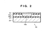
- a semiconductor substrate 50 as shown in Fig. 2 is finally obtained.
- the semiconductor substrate 50 shown in Fig. 2 has the partial insulating layer 14a under the single-crystal Si layer (first semiconductor layer) 13 and the full insulating layer 17 under and adjacent to or spaced apart from the partial insulating layer 14a.
- the full insulating layer 17 is arranged under and adjacent to the partial insulating layer 14a.
- a region without the partial insulating layer 14a has an SOI layer (to be referred to as a thick-SOI region hereinafter) thicker than that of a region with the partial insulating layer 14a.
- a first single-crystal Si substrate 11 of p-type or n-type having a resistivity of 0.01 to 0.02 ⁇ ⁇ cm was prepared (this corresponds to the step shown in Fig. 1A).
- the single-crystal Si substrate 11 was anodized in an anodizing solution, thereby forming a porous Si layer serving as a separation layer 12.
- the anodizing conditions were as follows.
- the current density and the concentrations of the respective components of the anodizing solution can appropriately be changed in accordance with the thickness, structure, and the like of the separation layer (porous Si layer) 12 to be formed.
- the current density falls within the range of 0 to 700 mA/cm 2
- the ratio between the concentrations of the above components of the anodizing solution falls within the range of 1 : 10 : 10 to 1 : 0 : 0.
- the porous Si layer is useful because a high-quality epitaxial Si layer is formed thereon and the porous Si layer functions as a separation layer. If the first and second substrates are bonded together to form a bonded substrate stack, and then the bonded substrate stack is ground to remove part of the first substrate, the porous Si layer need not be used as a separation layer.
- the anodizing solution only needs to contain HF and need not contain ethanol.
- Ethanol is useful for removing any air bubbles from the surface of the substrate and is preferably added to the anodizing solution.
- Examples of a chemical agent which has a function of removing air bubbles include, e.g., alcohols such as methyl alcohol and isopropyl alcohol, a surfactant, and the like in addition to ethanol. Instead of adding these chemical agents, air bubbles may be eliminated from the substrate surface by vibrations of ultrasonic waves or the like.
- the thickness of the porous Si layer is not limited to the above example. Satisfactory results can be obtained as far as the thickness falls within the range of, e . g . , several hundred ⁇ m to 0 .1 ⁇ m.
- the anodized substrate was oxidized in an oxygen atmosphere at 400°C for 1 hr. With this oxidizing step, the inner walls of pores of the porous Si layer were covered with a thermal oxide film.
- a single-crystal Si layer 13 having a thickness of 0.3 ⁇ m was epitaxially grown on the porous Si layer by chemical vapor deposition (CVD) (this corresponds to the step shown in Fig. 1C).
- the growth conditions were as follows.
- the substrate Prior to the epitaxial growth step, the substrate may be baked in an epitaxial reactor in a hydrogen atmosphere, and/or a minimum amount of silicon source may be supplied to the substrate in the epitaxial reactor. Then, the pores in the surface of the porous Si layer may be filled to planarize the substrate. By performing such an additional step, an epitaxial layer having a minimum defect density (10 4 cm -2 or less) could be formed on the porous Si layer.
- An SiO 2 layer 14 having a thickness of 200 nm was formed on the epitaxial Si layer 13 by thermal oxidation (this corresponds to the step shown in Fig. 1D).
- a mask material (preferably, SiN or the like) was deposited on the oxide film and a resist was further applied to its surface. These materials were sequentially patterned such that an opening was formed in a non-SOI region (or a thick-SOI region). Since this example uses a bonding method (e.g., ELTRAN: a registered trademark) in which the first substrate and second substrate are bonded together, patterning must be so performed as to form a mirror image of a normal pattern.
- ELTRAN a registered trademark
- a resist is applied to the SiO 2 layer 14 and is patterned to form a resist pattern. Then, the SiO 2 layer 14 is etched through an opening of the resist pattern to expose the epitaxial Si layer 13.
- a mask material is deposited on the SiO 2 layer 14, a resist is applied to the mask material and is patterned to form a resist pattern. Then, the mask material is etched through an opening of the resist pattern, thereby performing patterning for the mask material.
- the SiO 2 layer 14 is etched through an opening of the mask material until the epitaxial Si layer 13 is exposed, thereby performing patterning for the SiO 2 layer 14. At this time, the resist may be removed after the patterning of the mask material and before the patterning of the SiO 2 layer 14.
- a second epitaxial Si layer 15 was formed on the first epitaxial Si layer 13.
- a polysilicon layer 16 was formed on the SiO 2 layer 14a (this corresponds to the step shown in Fig. 1F).
- the thickness of the second epitaxial Si layer 15 can appropriately be determined in accordance with specifications required by a final semiconductor substrate. For example, the thickness can be set to 10 ⁇ m.
- polishing step CMP may be performed.
- a cleaning step and/or etching step may further be performed.
- the surface of a first substrate 10 and that of a second Si substrate 20 separately prepared were overlaid on and brought into contact with each other. After that, the both substrates were subjected to annealing in a nitrogen atmosphere or oxygen atmosphere at 1,100°C for 1 hr to increase the bonding strength between the first substrate 10 and the second substrate 20 (this corresponds to the step shown in Fig. 1H). With this operation, a bonded substrate stack 30 was obtained.
- a region in which a second epitaxial Si layer 15b is grown becomes not a non-SOI region but a thick-SOI region (see Fig. 2).
- the thickness of the silicon film in the thick-SOI region can appropriately be determined in accordance with specifications required by a final semiconductor substrate. For example, the thickness can be set to 10 ⁇ m.
- a region without any partial SiO 2 layer has not an SOI structure but the same structure as that of an epitaxial wafer (see Fig. 1K).
- Pure water was injected from a 0.1-mm nozzle of a water jet apparatus toward a concave portion (concave portion formed by the beveled portions of the two substrates 10 and 20) of the periphery of the bonded substrate stack 30 in a direction parallel to the bonding interface of the bonded substrate stack 30 at a high pressure of 50 MPa.
- the bonded substrate stack 30 was split at the separation layer 12 into two substrates (this corresponds to the step shown in Fig. 1I).
- the pressure of the pure water preferably falls within the range of, e.g., several MPa to 100 MPa.
- any one of the following operations may be performed.
- a jet of gas may be used or a solid wedge may be inserted into the separation layer of the bonded substrate stack.
- a mechanical force such as a tensile force, shearing force, or the like may be applied to the bonded substrate stack or ultrasonic waves may be applied to the bonded substrate stack.
- any other method may be adopted.
- a portion from the back surface of the first base 10 to the porous Si layer may be removed by grinding, polishing, etching, or the like without splitting the bonded substrate stack, thereby exposing the entire surface of the porous silicon layer.
- the porous Si layer 12b which was moved to the uppermost surface of the second substrate 20 was selectively etched using an etchant in which at least a 49% hydrofluoric acid solution, a 30% hydrogen peroxide solution, and water are mixed (this corresponds to the step shown in Fig. 1J).
- the single-crystal Si layer 13 was left unetched.
- the porous Si layer 12b was selectively etched using the single-crystal Si layer 13 as an etch stopper and completely removed. If selective etching is performed while starting/stopping generating ultrasonic waves using an apparatus combined with a circulator and rotating a wafer, non-uniform etching in the surface and among substrates can be suppressed. Additionally, if alcohol or a surfactant is mixed with the etchant, unevenness in etching caused by gaseous reaction products on the surface can be suppressed.
- the etching speed of a non-porous single-crystal Si layer with the etchant is extremely low, and the selectivity ratio to the etching speed of a porous layer reaches 10 5 or more.
- the etching amount (about several ten ⁇ ) in a non-porous layer reduces the film thickness by a substantially negligible amount.
- a semiconductor substrate which has the single-crystal Si layer 13 with a thickness of 0.2 ⁇ m on the partial insulating layer 14a and single-crystal Si layer 15 in the partial insulating layer 14a was obtained.
- the porous Si layer was selectively etched, no change occurred in the single-crystal Si layer 13.
- the uniformity of the film thickness was 201 nm ⁇ 4 nm.
- the substrate was subjected to annealing (hydrogen annealing) in a hydrogen atmosphere at 1,100°C for 1 hr, and the surface roughness was evaluated with an atomic force microscope.
- the root-mean-square roughness in a 50- ⁇ m-square region was about 0.2 nm, which was equivalent to that of a commercially available silicon wafer.
- the surface may be planarized by polishing such as CMP, instead of hydrogen annealing.
- the bonding strength can be increased even by annealing at a low temperature. Additionally, a substrate having undergone plasma processing is preferably rinsed by pure water.
- a plurality of bonded substrate stacks may be arranged in their planar direction, and a nozzle of a water jet apparatus may perform scanning along the planar direction, thereby continually splitting the plurality of bonded substrate stacks.
- a plurality of bonded substrate stacks may be arranged in a direction perpendicular to each plane, and a nozzle of a water jet apparatus may be provided with an X-Y scanning function. Then, a jet of water may sequentially be injected toward a plurality of bonding portions of the bonded substrate stack, and the bonded substrate stacks may automatically and continually be split.
- the single-crystal Si layer 13 and second semiconductor layer 15b may be made of, e.g., SiGe, GaAs, SiC, C, or the like, instead of single-crystal silicon.
- a substrate made of, e.g., quartz, sapphire, ceramic, carbon, SiC, or the like may be adopted, in addition to an Si substrate.
- This example is an improved example of the example 1 and is the same as the example 1 except for anodizing conditions.
- a single-crystal Si substrate 11 was prepared and anodized in a solution containing HF under either of the following anodizing conditions.
- the first porous Si layer to be formed at the first step of the anodization is used to form a high-quality epitaxial Si layer thereon.
- the second porous Si layer to be formed under the first porous Si layer at the second step of the anodization is used as a separation layer. Note that if the first substrate is removed by grinding a bonded substrate stack, a porous Si layer is not used as a separation layer.
- the position of a separation surface (a surface to be separated) was limited to the vicinity of the interface between the first porous Si layer and second porous Si layer. This was effective in planarization of the separation surface.
- a DRAM having a trench capacitor was formed in the non-SOI region of a semiconductor substrate which was manufactured by each of the methods described in the examples 1 and 2 and had a structure shown in Fig. 1K.
- Other devices including a logic circuit were formed in the SOI region.
- the methods described in the examples 1 and 2 are bonding methods, and the surface of a semiconductor substrate to be manufactured is flat. For this reason, in the lithography step, the entire region of exposure shots fell within the focus-range of the depth of a projection optical'system, and no local defocusing (defocusing due to unevenness of the surface of the substrate) occurred. Since a single-crystal Si layer having a sufficient thickness was formed in the non-SOI region, no trouble occurred in forming the trench capacitor.
- the above semiconductor substrate is effectively used to form an integrated circuit other than a DRAM-embedded one.
- Various film forming techniques such as CVD, MBE, sputtering, liquid phase growth can be applied to the epitaxial growth step for forming the first semiconductor layer and the second semiconductor layer.
- etchants e.g., a mixture of a hydrofluoric acid solution, nitric acid solution, and acetic acid solution
- a separation layer porous layer, ion implantation layer, or the like
- the present invention can, e.g., ensure the advantages of an SOI substrate for a substrate having a partial insulating layer under a semiconductor layer.
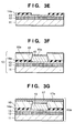
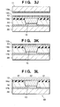
- Figs. 3A to 3L are views for explaining a substrate manufacturing method according to the second embodiment of the present invention.
- a single-crystal Si substrate (seed substrate) 11 is prepared, and in the step shown in Fig. 3B, a separation layer 12 is formed on the surface of the single-crystal Si substrate 11.
- the separation layer 12 e.g., a porous layer which can be formed by anodizing the surface of the single-crystal Si substrate 11 is preferably employed.
- This anodization can be performed by, e.g., placing an anode and cathode in an electrolyte solution containing hydrofluoric acid, placing the single-crystal Si substrate 11 between the electrodes, and supplying a current between them.
- the porous layer may comprise two or more layers with different porosities.
- a single-crystal Si layer (first semiconductor layer) 13 is formed on the separation layer 12 by epitaxial growth. Epitaxial growth can form the single-crystal Si layer 13 of good quality.
- a method of implanting ions such as hydrogen ions or the like at a predetermined depth from the surface of the single-crystal Si substrate 11 shown in Fig. 3A to form an ion implantation layer serving as the separation layer 12 may be adopted.
- a portion on the surface side from the viewpoint of the separation layer 12 functions as the single-crystal Si layer 13.
- a semiconductor layer made of another material may be formed on the separation layer 12.
- an SiO 2 layer 14 serving as an insulating layer is formed on the single-crystal Si layer 13.
- the SiO 2 layer 14 can be formed by, e.g., thermal oxidation. Thermal oxidation can form an SiO 2 layer of good quality.
- the SiO 2 layer 14 is patterned to form a partial SiO 2 layer 14a.
- a partial SiO 2 layer is defined as an SiO 2 layer which is formed such that the single-crystal Si layer (semiconductor layer) 13 is at least partially exposed.
- the SiO 2 layer 14 can be patterned by, e.g., the following operation. After a mask material is formed on the SiO 2 layer 14, the mask material is patterned by lithography (resist coating, exposure, development, and etching) to form an opening. The SiO 2 layer 14 exposed at the bottom of the opening is then etched by, e.g., reactive ion etching (RIE).
- RIE reactive ion etching
- a step of covering the surface except a region in which the partial SiO 2 layer 14a is to be formed with a mask pattern and forming the partial SiO 2 layer 14a only in an exposed portion may be adopted.
- a single-crystal Si layer (second semiconductor layer) 15 is grown by epitaxial growth on an exposed portion of the single-crystal Si layer 13 in the partial SiO 2 layer 14a.
- a polysilicon layer 16 may be formed on the partial insulating layer 14a.
- the single-crystal Si layer 15 and polysilicon layer 16 are different in growth rate, and a level difference may occur between the single-crystal Si layer 15 and the polysilicon layer 16, as exaggeratedly shown in Fig. 3F.
- Three-dimensional patterns 15a and 16a can be formed on the surfaces of the single-crystal Si layer 15 and polysilicon layer 16, respectively.
- a semiconductor layer made of another material is formed instead of the single-crystal Si layer 13.
- a semiconductor layer made of the same material as that of the formed semiconductor layer is preferably formed on the semiconductor layer in the step shown in Fig. 3F.
- a first substrate 10 is so formed as to have the single-crystal Si layer (first semiconductor layer) 13 on the porous layer or ion implantation layer as the separation layer 12, the partial SiO 2 layer (insulating layer) 14a on the single-crystal Si layer 13, and a single-crystal Si layer (second semiconductor layer) 15b on the single-crystal Si layer 13 and a polysilicon layer (second semiconductor layer) 16b on the insulating layer 14a.
- a substrate having a structure shown in Fig. 3F is referred to as the first substrate for the sake of convenience, a substrate having a structure shown in any one of Figs. 3A to 3E, 3G, and 3H may also be referred to as the first substrate.
- a third layer 17 is formed on the single-crystal Si layer 15 and polysilicon layer 16, i.e., the entire surface of the first substrate 10.
- the third layer preferably has a substantially uniform structure (structure which can uniformly be polished) to facilitate planarization in the subsequent planarizing step.
- the third layer 17 may comprise a semiconductor layer or a layer made of a material other than a semiconductor material.
- a polysilicon layer, an amorphous Si layer, an oxide film (e.g., an SiO 2 layer formed by CVD or the like), a PSG layer, a BPSG layer, or the like is preferably used.
- the SiO 2 layer may be formed by thermal oxidation, but CVD is more preferable. This is because thermal oxidation reflects the shape of an underlying layer in the surface shape of the SiO 2 layer while CVD tends to make the underlying layer have a more gently stepped surface.
- the formation of the third layer 17 can planarize the surface of a first substrate 10a. This contributes to an increase in bonding strength between the first and second substrates and ease of bonding, in the subsequent bonding step.
- the formation of the third layer 17 is also effective in keeping the single-crystal Si layers 13 and 15 finally serving as active layers away from the second substrate to be bonded to the first substrate.
- the surface of the first substrate 10 (see Fig. 3F), in which the single-crystal Si layer 15 and polysilicon layer 16 are combined, is preferably planarized by polishing, grinding, or the like before forming the third layer 17.
- the planarizing step need not be performed after the formation of the third layer 17.
- the step shown in Fig. 3H is a step performed when a three-dimensional pattern 17a on the surface of the first substrate 10a (see Fig. 3G) is inadmissibly uneven.
- the surface of the first substrate 10a is planarized by polishing, grinding, or the like. With this planarization of the third layer 17, the bonding strength between the first and second substrates and ease of bonding in the subsequent bonding step can further be increased.
- the step of planarizing the surface of the first substrate 10, in which the single-crystal Si layer 15 and polysilicon layer 16 are combined is performed without performing the formation step shown in Fig. 3G. Immediately after that, the first substrate is bonded to the second substrate.
- the second embodiment with the third layer is more preferable than the first embodiment without the third layer. More specifically, even if the planarizing step is performed for the surface of the first substrate 10, in which the single-crystal Si layer 15 and polysilicon layer 16 are combined, it is difficult to obtain good planarity.
- planarizing step suitable for the single-crystal Si layer 15 does not impart good planarity to the polysilicon layer 16 while the planarizing step suitable for the polysilicon layer 16 does not impart good planarity to the single-crystal Si layer 15. Additionally, a level difference may occur between the single-crystal Si layer 15 and polysilicon layer 16.
- a second substrate (handle substrate) 20 is bonded to the surface (a third layer 17b) of a first substrate 10b shown in Fig. 3H to form a bonded substrate stack 30.
- An SiO 2 layer may be formed on the surface of the first substrate 10 as the fourth layer by, e.g., thermal oxidation, prior to the bonding (except in cases in which the third layer comprises an insulting film such as an SiO 2 layer).
- the second substrate 20 a single-crystal Si substrate or a substrate obtained by forming an insulating layer such as an SiO 2 layer on the surface can typically be used.
- any other substrate such as an insulating substrate (e.g., a glass substrate) may be adopted as the second substrate 20.
- the bonded substrate stack 30 is split into two substrates by splitting the bonded substrate stack 30 at the separation layer 12.
- This splitting can be performed by, e.g., using a fluid.
- a method of using a fluid a method of forming a jet of a fluid (liquid or gas) and injecting it to the separation layer 12, a method of utilizing the static pressure of a fluid, or the like is preferably used.
- a method of utilizing water as a fluid is referred to as a water jet method.
- the above-mentioned splitting can also be performed by, e.g., annealing the bonded substrate stack 30. Such splitting by annealing is particularly effective in forming an ion implantation layer as the separation layer 12. Additionally, the splitting can be performed by, e.g., inserting a member such as a solid wedge into the separation layer 12.
- a grinding and polishing method in which the back surface (exposed surface) of the bonded substrate stack 30 is ground and polished to leave a single-crystal Si layer with a predetermined thickness on the insulating layer 14a may be adopted.
- the separation layer 12 need not be formed in advance.
- a separation layer 12b left on the single-crystal Si layer 13 of the second substrate 20 is removed using an etchant or the like.
- the single-crystal Si layer 13 can be used as an etching stopper layer.
- the surface of the substrate may be planarized by performing a planarizing step such as a hydrogen annealing step, polishing step, or the like, as needed.
- a semiconductor substrate (partial SOI substrate) 40 as shown in Fig. 3L is obtained.
- the semiconductor substrate 40 shown in Fig. 3L has the thin single-crystal Si layer (first semiconductor layer) 13 on its surface, the partial SiO 2 layer (insulating layer) 14a and single-crystal Si layer 15 under the single-crystal Si layer 13, and the third layer 17b under the partial SiO 2 layer 14a and single-crystal Si layer 15.
- a thin single-crystal Si layer means a layer thinner than a general semiconductor substrate.
- the thickness of the single-crystal Si layer (first semiconductor layer) 13 is preferably, e.g., 10 ⁇ m or less, and more preferably, 5 nm to 2 ⁇ m.
- a region (SOI region) 41 with the partial SiO 2 layer (insulating layer) 14a as a buried insulating layer out of the semiconductor substrate 40 has the same properties as those of an SOI substrate which has a buried insulating film over the whole region.
- the third layer 17b does not comprise an insulating layer such as an SiO 2 layer
- a region (non-SOI region) 42 without the partial insulating layer 14a out of the semiconductor substrate 40 i.e., a region which has the single-crystal Si layer 15 under the single-crystal Si layer 13 has substantially the same properties as those of an Si substrate which has an epitaxial Si layer on its surface.
- the single-crystal Si layer 15 is a layer which is formed by epitaxial growth using as the underlying layer the single-crystal Si layer 13 formed by epitaxial growth. For this reason, a defect hardly occurs in the interface between the single-crystal Si layer 13 and the single-crystal Si layer 15. Accordingly, if the semiconductor substrate 40 is used, a high-quality device can be formed even when a device (e.g., a trench capacitor) having a structure deeper than that of a device to be formed in the SOI region is formed in the non-SOI region.
- a device e.g., a trench capacitor
- the semiconductor substrate 40 has the partial insulating layer 14a under the single-crystal Si layer (first semiconductor layer) 13 and an insulating layer as the third layer 17b over the whole region under the partial insulating layer 14a (in the internal direction of the substrate).
- a region without the partial insulating layer 14a has an SOI layer (this region is to be referred to as a thick-SOI region hereinafter) thicker than that of a region with the partial insulating layer 14a.
- the semiconductor substrate 40 which can be manufactured by this embodiment is useful in forming a logic circuit in the SOI region 41 and forming a DRAM which has a trench-type capacitor in the non-SOI region 42.
- the semiconductor substrate 40 is useful in forming a memory cell transistor of a DRAM and a logic circuit on the SOI region 41 and forming a memory cell capacitor of the DRAM in the non-SOI region 42.
- Examples of the thicknesses of the single-crystal Si layer in the SOI and non-SOI regions in the semiconductor substrate 40 used to form a DRAM will be given.
- the single-crystal Si layer has a thickness of about 100 nm in the SOI region while it has a thickness of about several ⁇ m to 10 ⁇ m in the non-SOI region.
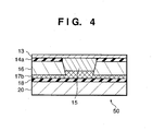
- the semiconductor substrate 50 shown in Fig. 4 has the partial insulating layer 14a under the single-crystal Si layer (first semiconductor layer) 13, the third layer 17b under the partial insulating layer 14a (in the internal direction of the substrate), and the insulating layer 18 under the third layer 17b.
- a region without the partial insulating layer 14a has an SOI layer (thick-SOI region) thicker than that of a region with the partial insulating layer 14a.
- a first single-crystal Si substrate 11 of p-type or n-type having a resistivity of 0.01 to 0.02 ⁇ ⁇ cm was prepared (this corresponds to the step shown in Fig. 3A).
- the single-crystal Si substrate 11 was anodized in an anodizing solution, thereby forming a porous Si layer serving as a separation layer 12.
- the anodizing conditions were as follows.
- the current density and the concentrations of the respective components of the anodizing solution can appropriately be changed in accordance with the thickness, structure, and the like of the separation layer (porous Si layer) 12 to be formed.
- the current density falls within the range of 0 to 700 mA/cm 2
- the ratio between the concentrations of the above components of the anodizing solution falls within the range of 1 : 10 : 10 to 1 : 0 : 0.
- the porous Si layer is useful because a high-quality epitaxial Si layer is formed thereon and the porous Si layer functions as a separation layer. If the first and second substrates are bonded together to form a bonded substrate stack, and then the bonded substrate stack is ground to remove part of the first substrate, the porous Si layer need not be used as a separation layer.
- the anodizing solution only needs to contain HF and need not contain ethanol.
- Ethanol is useful for removing any air bubbles from the surface of the substrate and is preferably added to the anodizing solution.
- Examples of a chemical agent which has a function of removing air bubbles include, e.g., alcohols such as methyl alcohol and isopropyl alcohol, a surfactant, and the like in addition to ethanol. Instead of adding these chemical agents, air bubbles may be eliminated from the substrate surface by vibrations of ultrasonic waves or the like.
- the thickness of the porous Si layer is not limited to the above example. Satisfactory results can be obtained as far as the thickness falls within the range of, e.g., several hundred ⁇ m to 0 .1 ⁇ m.
- the anodized substrate was oxidized in an oxygen atmosphere at 400°C for 1 hr. With this oxidizing step, the inner walls of pores of the porous Si layer were covered with a thermal oxide film.
- a single-crystal Si layer 13 having a thickness of 0.3 ⁇ m was epitaxially grown on the porous Si layer by chemical vapor deposition (CVD) (this corresponds to the step shown in Fig. 3C).
- the growth conditions were as follows.
- the substrate Prior to the epitaxial growth step, the substrate may be baked in an epitaxial reactor in a hydrogen atmosphere, and/or a minimum amount of silicon source may be supplied to the substrate in the epitaxial reactor. Then, the pores in the surface of the porous Si layer may be filled to planarize the substrate. By performing such an additional step, an epitaxial layer having a minimum defect density (10 4 cm -2 or less) could be formed on the porous Si layer.
- An SiO 2 layer 14 having a thickness of 200 nm was formed on the epitaxial Si layer 13 by thermal oxidation (this corresponds to the step shown in Fig. 3D).
- a mask material (preferably, SiN or the like) was deposited on the oxide film and a resist was further applied to its surface. These materials were sequentially patterned such that an opening was formed in a non-SOI region (or a thick-SOI region). Since this example uses a bonding method (e.g., ELTRAN: a registered trademark) in which the first substrate and second substrate are bonded together, patterning must be so performed as to form a mirror image of a normal pattern.
- ELTRAN a registered trademark
- a resist is applied to the SiO 2 layer 14 and is patterned to form a resist pattern. Then, the SiO 2 layer 14 is etched through an opening of the resist pattern to expose the epitaxial Si layer 13.
- a mask material is deposited on the SiO 2 layer 14, a resist is applied to the mask material and is patterned to form a resist pattern. Then, the mask material is etched through an opening of the resist pattern, thereby performing patterning for the mask material.
- the SiO 2 layer 14 is etched through an opening of the mask material until the epitaxial Si layer 13 is exposed, thereby performing patterning for the SiO 2 layer 14. At this time, the resist may be removed after the patterning of the mask material and before the patterning of the SiO 2 layer 14.
- a second epitaxial Si layer 15 was formed on the first epitaxial Si layer 13.
- a polysilicon layer 16 was formed on the SiO 2 layer 14a (this corresponds to the step shown in Fig. 3F).
- the thickness of the second epitaxial Si layer 15 can appropriately be determined in accordance with specifications required by a final semiconductor substrate. For example, the thickness can be set to 10 ⁇ m.
- a polysilicon layer having a thickness of 3 ⁇ m was grown as a third layer 17 on the entire surface of a first substrate 10 (this corresponds to the step shown in Fig. 3G).
- the thickness of the third layer can be changed in accordance with required planarity or the like of the first substrate.
- an insulating layer such as an amorphous Si layer, an oxide film (e.g., an SiO 2 layer formed by CVD or the like), a PSG layer, a BPSG layer, or the like in addition to a polysilicon layer is preferably used.
- An insulating layer such as an SiO 2 layer may be formed as the fourth layer on the third layer 17 (except in cases in which the third layer comprises an insulting layer).
- the surface (third layer 17) of a first substrate 10a was planarized by polishing (this corresponds to the step shown in Fig. 3H).
- CMP may be performed.
- a cleaning step and/or etching step may further be performed.
- the surface of a first substrate 10b and that of a second Si substrate 20 separately prepared were overlaid on and brought into contact with each other. After that, the both substrates were subjected to annealing in a nitrogen atmosphere or oxygen atmosphere at 1,100°C for 1 hr to increase the bonding strength between the first substrate 10 and the second substrate 20 (this corresponds to the step shown in Fig. 3I). With this operation, a bonded substrate stack 30 was obtained.
- the third layer of the first substrate 10 comprises an insulating layer
- an insulating layer is formed as the fourth layer on the third layer, or if at least the surface of the second substrate 20 comprises an insulator
- a region in which a second epitaxial Si layer 15b is grown becomes not a non-SOI region but a thick-SOI region (see Fig. 4).
- the thickness of the silicon film in the thick-SOI region can appropriately be determined in accordance with specifications required by a final semiconductor substrate. For example, the thickness can be set to 10 ⁇ m.
- a region without any partial SiO 2 layer has not an SOI structure but the same structure as that of an epitaxial wafer (see Fig. 3L).
- Pure water was injected from a 0.1-mm nozzle of a water jet apparatus toward a concave portion (concave portion formed by the beveled portions of the two substrates 10 and 20) of the periphery of the bonded substrate stack 30 in a direction parallel to the bonding interface of the bonded substrate stack 30 at a high pressure of 50 MPa.
- the bonded substrate stack 30 was split at the separation layer 12 into two substrates (this corresponds to the step shown in Fig. 3J).
- the pressure of the pure water preferably falls within the range of, e.g., several MPa to 100 MPa.
- any one of the following operations may be performed.
- a jet of gas may be used or a solid wedge may be inserted into the separation layer of the bonded substrate stack.
- a mechanical force such as a tensile force, shearing force, or the like may be applied to the bonded substrate stack or ultrasonic waves may be applied to the bonded substrate stack.
- any other method may be adopted.
- a portion from the back surface of the first base 10 to the porous Si layer may be removed by grinding, polishing, etching, or the like without splitting the bonded substrate stack, thereby exposing the entire surface of the porous silicon layer.
- the porous Si layer 12b which was moved to the uppermost surface of the second substrate 20 was selectively etched using an etchant in which at least a 49% hydrofluoric acid solution, a 30% hydrogen peroxide solution, and water are mixed (this corresponds to the step shown in Fig. 3K).
- the single-crystal Si layer 13 was left unetched.
- the porous Si layer 12b was selectively etched using the single-crystal Si layer 13 as an etch stopper and completely removed. If selective etching is performed while starting/stopping generating ultrasonic waves using an apparatus combined with a circulator and rotating a wafer, non-uniform etching in the surface and among substrates can be suppressed. Additionally, if alcohol or a surfactant is mixed with the etchant, unevenness in etching caused by gaseous reaction products on the surface can be suppressed.
- the etching speed of a non-porous single-crystal Si layer with the etchant is extremely low, and the selectivity ratio to the etching speed of a porous layer reaches 10 5 or more.
- the etching amount (about several ten ⁇ ) in a non-porous layer reduces the film thickness by a substantially negligible amount.
- a semiconductor substrate which has the single-crystal Si layer 13 with a thickness of 0.2 ⁇ m on the partial insulating layer 14a and single-crystal Si layer 15 in the partial insulating layer 14a was obtained.
- the porous Si layer was selectively etched, no change occurred in the single-crystal Si layer 13.
- the uniformity of the film thickness was 201 nm ⁇ 4 nm.
- the substrate was subjected to annealing (hydrogen annealing) in a hydrogen atmosphere at 1,100°C for 1 hr, and the surface roughness was evaluated with an atomic force microscope.
- the root-mean-square roughness in a 50- ⁇ m-square region was about 0.2 nm, which was equivalent to that of a commercially available silicon wafer.
- the surface may be planarized by polishing such as CMP, instead of hydrogen annealing.
- the bonding strength can be increased even by annealing at a low temperature. Additionally, a substrate having undergone plasma processing is preferably rinsed by pure water.
- a plurality of bonded substrate stacks may be arranged in their planar direction, and a nozzle of a water jet apparatus may perform scanning along the planar direction, thereby continually splitting the plurality of bonded substrate stacks.
- a plurality of bonded substrate stacks may be arranged in a direction perpendicular to each plane, and a nozzle of a water jet apparatus may be provided with an X-Y scanning function. Then, a jet of water may sequentially be injected toward a plurality of bonding portions of the bonded substrate stack, and the bonded substrate stacks may automatically and continually be split.
- the single-crystal Si layer 13 and second semiconductor layer 15 may be made of, e.g., SiGe, GaAs, SiC, C, or the like, instead of single-crystal silicon.
- a substrate made of, e.g., quartz, sapphire, ceramic, carbon, SiC, or the like may be adopted, in addition to an Si substrate.
- This example is an improved example of the example 1 and is the same as the example 1 except for anodizing conditions.
- a single-crystal Si substrate 11 was prepared and anodized in a solution containing HF under either of the following anodizing conditions.
- the first porous Si layer to be formed at the first step of the anodization is used to form a high-quality epitaxial Si layer thereon.
- the second porous Si layer to be formed under the first porous Si layer at the second step of the anodization is used as a separation layer. Note that if the first substrate is removed by grinding a bonded substrate stack, a porous Si layer is not used as a separation layer.
- the position of a separation surface (a surface to be separated) was limited to the vicinity of the interface between the first porous Si layer and second porous Si layer. This was effective in planarization of the separation surface.
- a DRAM having a trench capacitor was formed in the non-SOI region of a semiconductor substrate which was manufactured by each of the methods described in the examples 1 and 2 and had a structure shown in Fig. 3L.
- Other devices including a logic circuit were formed in the SOI region.
- the methods described in the examples 1 and 2 are bonding methods, and the surface of a semiconductor substrate to be manufactured is flat. For this reason, in the lithography step, the entire region of exposure shots fell within the focus-range of the depth of a projection optical system, and no local defocusing (defocusing due to unevenness of the surface of the substrate) occurred. Since a single-crystal Si layer having a sufficient thickness was formed in the non-SOI region, no trouble occurred in forming the trench capacitor.
- the above semiconductor substrate is effectively used to form an integrated circuit other than a DRAM-embedded one.
- Various film forming techniques such as CVD, MBE, sputtering, liquid phase growth can be applied to the epitaxial growth step for forming the first semiconductor layer and the second semiconductor layer.
- etchants e.g., a mixture of a hydrofluoric acid solution, nitric acid solution, and acetic acid solution
- a separation layer porous layer, ion implantation layer, or the like
- the present invention can, e.g., improve the quality of a substrate to be manufactured through a step of bonding two substrates.
- a partial SOI substrate (40) is obtained by performing steps of forming the first substrate which has a separation layer, the first semiconductor layer (13) on the separation layer, a partial insulating layer (14a) on the first semiconductor layer (13), and second semiconductor layers (15b, 16b) on the first semiconductor layer (13) exposed in the partial insulating layer (14a) and partial insulating layer (14a), bonding the second substrate (20) to the second semiconductor layers (15b, 16b) on the first substrate to form a bonded substrate stack, and splitting the bonded substrate stack at the separation layer.
Landscapes
- Element Separation (AREA)
- Recrystallisation Techniques (AREA)
- Thin Film Transistor (AREA)
Abstract
Description
or
or
Claims (29)
- A substrate manufacturing method comprising:a step of forming a first substrate which has a separation layer, a first semiconductor layer on the separation layer, a partial insulating layer on the first semiconductor layer, and a second semiconductor layer on the first semiconductor layer exposed in the partial insulating layer and the partial insulating layer;a step of bonding a second substrate to the second semiconductor layer on the first substrate to form a bonded substrate stack; anda step of splitting the bonded substrate stack at the separation layer.
- The method according to claim 1, further comprising a step of planarizing the second semiconductor layer of the first substrate before bonding the second substrate to the second semiconductor layer on the first substrate.
- The method according to claim 1, wherein in growing the second semiconductor layer, a single-crystal semiconductor layer made of the same material as a material of the first semiconductor layer is grown as a part of the second semiconductor layer on the first semiconductor layer exposed in the insulating layer.
- The method according to claim 1, wherein in growing the second semiconductor layer, a single-crystal semiconductor layer made of the same material as a material of the first semiconductor layer is grown as a part of the second semiconductor layer on the first semiconductor layer exposed in the insulating layer, and a polycrystalline semiconductor layer made of the same material as a material of the first semiconductor layer is grown as another part of the second semiconductor layer on the partial insulating layer.
- The method according to claim 1, wherein the step of forming the first substrate includes a step of forming a porous layer serving as the separation layer on a semiconductor substrate by anodization and sequentially forming the first semiconductor layer and partial insulating layer on the porous layer.
- The method according to claim 1, wherein the step of forming the first substrate includes a step of forming the separation layer by implanting ions into a semiconductor substrate.
- The method according to claim 1, wherein at least a surface, to be bonded to the first substrate, of the second substrate comprises an insulator.
- A substrate manufacturing method comprising:a step of forming a first substrate which has a first semiconductor layer, a partial insulating layer on the first semiconductor layer, and a second semiconductor layer on the first semiconductor layer exposed in the partial insulating layer and the partial insulating layer;a step of bonding a second substrate to the second semiconductor layer on the first substrate to form a bonded substrate stack; anda step of grinding the first substrate constituting a part of the bonded substrate stack from a back surface of the first substrate to thin the bonded substrate stack.
- A substrate which can be manufactured by a manufacturing method as defined in claim 1.
- A substrate which can be manufactured by a manufacturing method as defined in claim 8.
- A substrate comprising:a first insulating layer arranged over a whole region inside the substrate;a second partial insulating layer arranged adjacent to or spaced apart from the said first insulating layer, on said first insulating layer; anda semiconductor layer arranged on a surface of the substrate.
- A substrate manufacturing method comprising:a step of forming a first substrate which has a first semiconductor layer, a partial insulating layer on the first semiconductor layer, and a second semiconductor layer on the first semiconductor layer exposed in the partial insulating layer and the partial insulating layer;a step of forming a third layer on an entire surface of the second semiconductor layer of the first substrate; anda step of bonding a second substrate to the third layer of the first substrate to form a bonded substrate stack.
- The method according to claim 12, further comprising a step of removing a part of the first substrate from the bonded substrate stack such that the first semiconductor layer is exposed.
- The method according to claim 12, wherein
the step of forming the first substrate includes a step of forming a separation layer under the first semiconductor layer, and
the method further comprises a step of splitting the bonded substrate stack at the separation layer. - The method according to claim 12, further comprising a step of planarizing a surface of the third layer after the step of forming the third layer and before the step of forming the bonded substrate stack.
- The method according to claim 12, further comprising a step of planarizing a surface of the second semiconductor layer after the step of forming the first substrate and before the step of forming the third layer.
- The method according to claim 12, wherein in the step of forming the third layer, a layer having a structure substantially uniform across a surface of the layer is formed as the third layer.
- The method according to claim 12, wherein in the step of forming the third layer, a polycrystalline semiconductor layer is formed as the third layer.
- The method according to claim 12, wherein in the step of forming the third layer, an amorphous semiconductor layer is formed as the third layer.
- The method according to claim 12, wherein in the step of forming the third layer, an insulating layer is formed as the third layer.
- The method according to claim 20, wherein the insulating layer comprises an oxide film.
- The method according to claim 20, wherein in the step of forming the third layer, the oxide film is formed by CVD.
- The method according to claim 12, wherein in growing the second semiconductor layer, a single-crystal semiconductor layer made of the same material as a material of the first semiconductor layer is grown as a part of the second semiconductor layer on the first semiconductor layer exposed in the insulating layer.
- The method according to claim 12, wherein in growing the second semiconductor layer, a single-crystal semiconductor layer made of the same material as a material of the first semiconductor layer is grown as a part of the second semiconductor layer on the first semiconductor layer exposed in the insulating layer, and a polycrystalline semiconductor layer made of the same material as the first semiconductor layer is grown as another part of the second semiconductor layer on the partial insulating layer.
- The method according to claim 12, wherein the step of forming the first substrate includes a step of forming a porous layer serving as the separation layer on a semiconductor substrate by anodization and sequentially forming the first semiconductor layer and partial insulating layer on the porous layer.
- A substrate which can be manufactured by a manufacturing method as defined in claim 12.
- A substrate comprising:a first semiconductor layer arranged on a surface of the substrate;a first partial insulating layer arranged under said first semiconductor layer;a second semiconductor layer arranged adjacent to and under said first semiconductor layer in said first partial insulating layer and said first partial insulating layer; anda third layer arranged adjacent to and under said second semiconductor layer.
- The method according to claim 27, wherein said third layer has a lower planarized surface.
- The method according to claim 27, further comprising a handle substrate arranged adjacent to or under said third layer through a fourth layer.
Applications Claiming Priority (4)
| Application Number | Priority Date | Filing Date | Title |
|---|---|---|---|
| JP2002258973A JP2004103602A (en) | 2002-09-04 | 2002-09-04 | Substrate and method of manufacturing the same |
| JP2002258972 | 2002-09-04 | ||
| JP2002258972A JP2004103601A (en) | 2002-09-04 | 2002-09-04 | Substrate and method of manufacturing the same |
| JP2002258973 | 2002-09-04 |
Publications (2)
| Publication Number | Publication Date |
|---|---|
| EP1396883A2 true EP1396883A2 (en) | 2004-03-10 |
| EP1396883A3 EP1396883A3 (en) | 2005-11-30 |
Family
ID=31719907
Family Applications (1)
| Application Number | Title | Priority Date | Filing Date |
|---|---|---|---|
| EP03020006A Withdrawn EP1396883A3 (en) | 2002-09-04 | 2003-09-03 | Substrate and manufacturing method therefor |
Country Status (3)
| Country | Link |
|---|---|
| US (1) | US6951796B2 (en) |
| EP (1) | EP1396883A3 (en) |
| TW (1) | TWI242796B (en) |
Families Citing this family (20)
| Publication number | Priority date | Publication date | Assignee | Title |
|---|---|---|---|---|
| JP2004103600A (en) * | 2002-09-04 | 2004-04-02 | Canon Inc | Substrate and method of manufacturing the same |
| JP2004103855A (en) * | 2002-09-10 | 2004-04-02 | Canon Inc | Substrate and method of manufacturing the same |
| JP2004103946A (en) * | 2002-09-11 | 2004-04-02 | Canon Inc | Substrate and method of manufacturing the same |
| US20060110580A1 (en) * | 2003-04-28 | 2006-05-25 | Aylward Peter T | Article comprising conductive conduit channels |
| US7161169B2 (en) * | 2004-01-07 | 2007-01-09 | International Business Machines Corporation | Enhancement of electron and hole mobilities in <110> Si under biaxial compressive strain |
| EP1605502A1 (en) * | 2004-06-08 | 2005-12-14 | Interuniversitair Microelektronica Centrum Vzw | Transfer method for the manufacturing of electronic devices |
| JP2006041135A (en) * | 2004-07-26 | 2006-02-09 | Sumitomo Bakelite Co Ltd | Electronic device and manufacturing method thereof |
| FR2875947B1 (en) * | 2004-09-30 | 2007-09-07 | Tracit Technologies | NOVEL STRUCTURE FOR MICROELECTRONICS AND MICROSYSTEMS AND METHOD OF MAKING SAME |
| US7547605B2 (en) * | 2004-11-22 | 2009-06-16 | Taiwan Semiconductor Manufacturing Company | Microelectronic device and a method for its manufacture |
| TW200644165A (en) * | 2005-05-04 | 2006-12-16 | Icemos Technology Corp | Silicon wafer having through-wafer vias |
| US20080099924A1 (en) * | 2005-05-04 | 2008-05-01 | Icemos Technology Corporation | Silicon Wafer Having Through-Wafer Vias With A Predetermined Geometric Shape |
| US7166520B1 (en) * | 2005-08-08 | 2007-01-23 | Silicon Genesis Corporation | Thin handle substrate method and structure for fabricating devices using one or more films provided by a layer transfer process |
| FR2897982B1 (en) * | 2006-02-27 | 2008-07-11 | Tracit Technologies Sa | METHOD FOR MANUFACTURING PARTIALLY-LIKE STRUCTURES, COMPRISING AREAS CONNECTING A SURFACE LAYER AND A SUBSTRATE |
| TW200818534A (en) * | 2006-08-10 | 2008-04-16 | Icemos Technology Corp | Method of manufacturing a photodiode array with through-wafer vias |
| EP1959490A1 (en) * | 2007-02-15 | 2008-08-20 | Stmicroelectronics SA | Method of manufacturing a semiconductor-type structure on an insulator |
| US7772054B2 (en) * | 2007-06-15 | 2010-08-10 | Semiconductor Energy Laboratory Co., Ltd. | Method for manufacturing semiconductor device |
| JP4979732B2 (en) | 2009-05-01 | 2012-07-18 | 信越化学工業株式会社 | Manufacturing method of bonded wafer |
| JP5505367B2 (en) * | 2011-05-11 | 2014-05-28 | 信越半導体株式会社 | Method for manufacturing bonded substrate having insulating layer on part of substrate |
| CN108346686B (en) * | 2017-01-25 | 2021-07-30 | 中芯国际集成电路制造(上海)有限公司 | Semiconductor device and method of manufacturing the same |
| SG11201913769RA (en) * | 2017-07-14 | 2020-01-30 | Sunedison Semiconductor Ltd | Method of manufacture of a semiconductor on insulator structure |
Family Cites Families (55)
| Publication number | Priority date | Publication date | Assignee | Title |
|---|---|---|---|---|
| US3372063A (en) * | 1964-12-22 | 1968-03-05 | Hitachi Ltd | Method for manufacturing at least one electrically isolated region of a semiconductive material |
| US5362682A (en) * | 1980-04-10 | 1994-11-08 | Massachusetts Institute Of Technology | Method of producing sheets of crystalline material and devices made therefrom |
| US5328549A (en) * | 1980-04-10 | 1994-07-12 | Massachusetts Institute Of Technology | Method of producing sheets of crystalline material and devices made therefrom |
| JPS5861622A (en) * | 1981-10-09 | 1983-04-12 | Hitachi Ltd | Manufacture of single crystal thin film |
| US4549926A (en) * | 1982-01-12 | 1985-10-29 | Rca Corporation | Method for growing monocrystalline silicon on a mask layer |
| US4585493A (en) * | 1984-06-26 | 1986-04-29 | General Electric Company | Grain-driven zone-melting of silicon films on insulating substrates |
| FR2571544B1 (en) * | 1984-10-05 | 1987-07-31 | Haond Michel | PROCESS FOR MANUFACTURING ELECTRICALLY ISOLATED MONOCRYSTALLINE SILICON ISLANDS FROM EACH OTHER |
| US5086011A (en) * | 1987-01-27 | 1992-02-04 | Advanced Micro Devices, Inc. | Process for producing thin single crystal silicon islands on insulator |
| US4851078A (en) | 1987-06-29 | 1989-07-25 | Harris Corporation | Dielectric isolation process using double wafer bonding |
| JPS6432622A (en) * | 1987-07-28 | 1989-02-02 | Mitsubishi Electric Corp | Formation of soi film |
| US4963505A (en) | 1987-10-27 | 1990-10-16 | Nippondenso Co., Ltd. | Semiconductor device and method of manufacturing same |
| JP2794702B2 (en) | 1987-11-30 | 1998-09-10 | 株式会社デンソー | Method for manufacturing semiconductor device |
| US5138422A (en) | 1987-10-27 | 1992-08-11 | Nippondenso Co., Ltd. | Semiconductor device which includes multiple isolated semiconductor segments on one chip |
| JP2643262B2 (en) * | 1988-03-23 | 1997-08-20 | 日本電気株式会社 | Method for manufacturing semiconductor device |
| FR2629636B1 (en) * | 1988-04-05 | 1990-11-16 | Thomson Csf | METHOD FOR PRODUCING AN ALTERNATION OF LAYERS OF SINGLE-CRYSTAL SEMICONDUCTOR MATERIAL AND LAYERS OF INSULATING MATERIAL |
| FR2640428B1 (en) * | 1988-12-09 | 1992-10-30 | Thomson Csf | METHOD OF HARDENING WITH RESPECT TO IONIZING RADIATION OF ACTIVE ELECTRONIC COMPONENTS, AND HARDENED COMPONENTS OF LARGE DIMENSIONS |
| SG59963A1 (en) | 1990-08-03 | 1999-02-22 | Canon Kk | Semiconductor member and process for preparing semiconductor member |
| US5403751A (en) * | 1990-11-29 | 1995-04-04 | Canon Kabushiki Kaisha | Process for producing a thin silicon solar cell |
| US5403771A (en) | 1990-12-26 | 1995-04-04 | Canon Kabushiki Kaisha | Process for producing a solar cell by means of epitaxial growth process |
| JP2690412B2 (en) | 1991-06-11 | 1997-12-10 | ローム株式会社 | Method of manufacturing semiconductor device having growth layer on insulating layer |
| FR2681472B1 (en) | 1991-09-18 | 1993-10-29 | Commissariat Energie Atomique | PROCESS FOR PRODUCING THIN FILMS OF SEMICONDUCTOR MATERIAL. |
| JP3237888B2 (en) * | 1992-01-31 | 2001-12-10 | キヤノン株式会社 | Semiconductor substrate and method of manufacturing the same |
| JPH05251292A (en) | 1992-03-06 | 1993-09-28 | Nec Corp | Manufacture of semiconductor device |
| JPH06267848A (en) * | 1993-03-10 | 1994-09-22 | Shin Etsu Handotai Co Ltd | Epitaxial wafer and manufacturing method thereof |
| JPH1027893A (en) * | 1993-10-29 | 1998-01-27 | Amer Fib Inc | An integrated circuit (IC) device provided on a SOI wafer having a separately formed doped region electrically coupled into the substrate below an insulating layer provided as a charge sink or potential well |
| JPH07161936A (en) * | 1993-12-07 | 1995-06-23 | Toshiba Corp | Semiconductor memory device and manufacturing method thereof |
| JP3257580B2 (en) | 1994-03-10 | 2002-02-18 | キヤノン株式会社 | Manufacturing method of semiconductor substrate |
| JP3293736B2 (en) | 1996-02-28 | 2002-06-17 | キヤノン株式会社 | Semiconductor substrate manufacturing method and bonded substrate |
| US6103598A (en) | 1995-07-13 | 2000-08-15 | Canon Kabushiki Kaisha | Process for producing semiconductor substrate |
| EP0755068B1 (en) | 1995-07-21 | 2003-06-04 | Canon Kabushiki Kaisha | Semiconductor substrate and process for production thereof |
| EP0757377B1 (en) | 1995-08-02 | 2003-04-09 | Canon Kabushiki Kaisha | Semiconductor substrate and fabrication method for the same |
| CN1132223C (en) | 1995-10-06 | 2003-12-24 | 佳能株式会社 | Semiconductor substrate and producing method thereof |
| US5710057A (en) * | 1996-07-12 | 1998-01-20 | Kenney; Donald M. | SOI fabrication method |
| SG55413A1 (en) | 1996-11-15 | 1998-12-21 | Method Of Manufacturing Semico | Method of manufacturing semiconductor article |
| US6054363A (en) | 1996-11-15 | 2000-04-25 | Canon Kabushiki Kaisha | Method of manufacturing semiconductor article |
| SG65697A1 (en) | 1996-11-15 | 1999-06-22 | Canon Kk | Process for producing semiconductor article |
| EP0849788B1 (en) | 1996-12-18 | 2004-03-10 | Canon Kabushiki Kaisha | Process for producing semiconductor article by making use of a substrate having a porous semiconductor layer |
| SG68035A1 (en) | 1997-03-27 | 1999-10-19 | Canon Kk | Method and apparatus for separating composite member using fluid |
| US6191007B1 (en) | 1997-04-28 | 2001-02-20 | Denso Corporation | Method for manufacturing a semiconductor substrate |
| US6159824A (en) | 1997-05-12 | 2000-12-12 | Silicon Genesis Corporation | Silicon-on-silicon wafer bonding process using a thin film blister-separation method |
| US5894152A (en) | 1997-06-18 | 1999-04-13 | International Business Machines Corporation | SOI/bulk hybrid substrate and method of forming the same |
| WO1999001594A1 (en) * | 1997-07-03 | 1999-01-14 | Cbl Technologies | Thermal mismatch compensation to produce free standing substrates by epitaxial deposition |
| FR2774511B1 (en) | 1998-01-30 | 2002-10-11 | Commissariat Energie Atomique | SUBSTRATE COMPLIANT IN PARTICULAR FOR A DEPOSIT BY HETERO-EPITAXY |
| MY118019A (en) | 1998-02-18 | 2004-08-30 | Canon Kk | Composite member, its separation method, and preparation method of semiconductor substrate by utilization thereof |
| EP1100124A4 (en) * | 1998-06-26 | 2007-05-02 | Mitsubishi Material Silicon | DIELECTRIC SEPARATION WAFER AND METHOD FOR MANUFACTURING THE SAME |
| JP3525061B2 (en) * | 1998-09-25 | 2004-05-10 | 株式会社東芝 | Method for manufacturing semiconductor light emitting device |
| US6331473B1 (en) * | 1998-12-29 | 2001-12-18 | Seiko Epson Corporation | SOI substrate, method for making the same, semiconductive device and liquid crystal panel using the same |
| JP2001015721A (en) | 1999-04-30 | 2001-01-19 | Canon Inc | Method for separating composite member and method for producing thin film |
| JP3555500B2 (en) | 1999-05-21 | 2004-08-18 | 豊田合成株式会社 | Group III nitride semiconductor and method of manufacturing the same |
| US6323108B1 (en) | 1999-07-27 | 2001-11-27 | The United States Of America As Represented By The Secretary Of The Navy | Fabrication ultra-thin bonded semiconductor layers |
| US6602767B2 (en) | 2000-01-27 | 2003-08-05 | Canon Kabushiki Kaisha | Method for transferring porous layer, method for making semiconductor devices, and method for making solar battery |
| KR100356577B1 (en) | 2000-03-30 | 2002-10-18 | 삼성전자 주식회사 | SOI SUBSTRATE and its manufacturing method and SOI MOSFET using THE SAME |
| JP2001320033A (en) | 2000-05-10 | 2001-11-16 | Canon Inc | Semiconductor member manufacturing method, semiconductor member using the same, and semiconductor device |
| US7186630B2 (en) * | 2002-08-14 | 2007-03-06 | Asm America, Inc. | Deposition of amorphous silicon-containing films |
| JP2004103855A (en) | 2002-09-10 | 2004-04-02 | Canon Inc | Substrate and method of manufacturing the same |
-
2003
- 2003-09-03 TW TW092124376A patent/TWI242796B/en not_active IP Right Cessation
- 2003-09-03 EP EP03020006A patent/EP1396883A3/en not_active Withdrawn
- 2003-09-04 US US10/653,950 patent/US6951796B2/en not_active Expired - Fee Related
Also Published As
| Publication number | Publication date |
|---|---|
| US6951796B2 (en) | 2005-10-04 |
| TW200406819A (en) | 2004-05-01 |
| EP1396883A3 (en) | 2005-11-30 |
| TWI242796B (en) | 2005-11-01 |
| US20040058511A1 (en) | 2004-03-25 |
Similar Documents
| Publication | Publication Date | Title |
|---|---|---|
| US6951796B2 (en) | Substrate and manufacturing method therefor | |
| US6946354B2 (en) | Substrate and manufacturing method therefor | |
| US7341923B2 (en) | Substrate, manufacturing method therefor, and semiconductor device | |
| US6376332B1 (en) | Composite member and separating method therefor, bonded substrate stack and separating method therefor, transfer method for transfer layer, and SOI substrate manufacturing method | |
| US6624047B1 (en) | Substrate and method of manufacturing the same | |
| US6426270B1 (en) | Substrate processing method and method of manufacturing semiconductor substrate | |
| EP1398825A2 (en) | Substrate and manufacturing method therefor | |
| EP0989593A2 (en) | Substrate separating apparatus and method, and substrate manufacturing method | |
| KR100238571B1 (en) | Manufacturing method of semiconductor substrate | |
| US7928436B2 (en) | Methods for forming germanium-on-insulator semiconductor structures using a porous layer and semiconductor structures formed by these methods | |
| JP3352340B2 (en) | Semiconductor substrate and method of manufacturing the same | |
| US20020048844A1 (en) | Semiconductor substrate, method of manufacturing the same, and bonded substrate stack surface shape measuring method | |
| US7368332B2 (en) | SOI substrate manufacturing method | |
| EP1197987A2 (en) | Method and apparatus for separating sample | |
| US20040040492A1 (en) | Substrate and manufacturing method therefor | |
| US11610808B2 (en) | Semiconductor wafer with low defect count and method for manufacturing thereof | |
| JP2000188269A (en) | Member separating method and separating apparatus, and substrate manufacturing method | |
| JP2004103602A (en) | Substrate and method of manufacturing the same | |
| US20050266657A1 (en) | Substrate manufacturing method | |
| JP2004103801A (en) | Substrate and method of manufacturing the same | |
| JP2004103601A (en) | Substrate and method of manufacturing the same | |
| JPH09307084A (en) | Method for forming semiconductor substrate |
Legal Events
| Date | Code | Title | Description |
|---|---|---|---|
| PUAI | Public reference made under article 153(3) epc to a published international application that has entered the european phase |
Free format text: ORIGINAL CODE: 0009012 |
|
| AK | Designated contracting states |
Kind code of ref document: A2 Designated state(s): AT BE BG CH CY CZ DE DK EE ES FI FR GB GR HU IE IT LI LU MC NL PT RO SE SI SK TR |
|
| AX | Request for extension of the european patent |
Extension state: AL LT LV MK |
|
| PUAL | Search report despatched |
Free format text: ORIGINAL CODE: 0009013 |
|
| AK | Designated contracting states |
Kind code of ref document: A3 Designated state(s): AT BE BG CH CY CZ DE DK EE ES FI FR GB GR HU IE IT LI LU MC NL PT RO SE SI SK TR |
|
| AX | Request for extension of the european patent |
Extension state: AL LT LV MK |
|
| AKX | Designation fees paid |
Designated state(s): DE FR |
|
| STAA | Information on the status of an ep patent application or granted ep patent |
Free format text: STATUS: THE APPLICATION IS DEEMED TO BE WITHDRAWN |
|
| 18D | Application deemed to be withdrawn |
Effective date: 20060531 |