EP1396878A1 - Production method for semiconductor substrate and semiconductor element - Google Patents
Production method for semiconductor substrate and semiconductor element Download PDFInfo
- Publication number
- EP1396878A1 EP1396878A1 EP02707196A EP02707196A EP1396878A1 EP 1396878 A1 EP1396878 A1 EP 1396878A1 EP 02707196 A EP02707196 A EP 02707196A EP 02707196 A EP02707196 A EP 02707196A EP 1396878 A1 EP1396878 A1 EP 1396878A1
- Authority
- EP
- European Patent Office
- Prior art keywords
- semiconductor
- crystal
- reaction prevention
- producing
- prevention layer
- Prior art date
- Legal status (The legal status is an assumption and is not a legal conclusion. Google has not performed a legal analysis and makes no representation as to the accuracy of the status listed.)
- Withdrawn
Links
Images


Classifications
-
- C—CHEMISTRY; METALLURGY
- C23—COATING METALLIC MATERIAL; COATING MATERIAL WITH METALLIC MATERIAL; CHEMICAL SURFACE TREATMENT; DIFFUSION TREATMENT OF METALLIC MATERIAL; COATING BY VACUUM EVAPORATION, BY SPUTTERING, BY ION IMPLANTATION OR BY CHEMICAL VAPOUR DEPOSITION, IN GENERAL; INHIBITING CORROSION OF METALLIC MATERIAL OR INCRUSTATION IN GENERAL
- C23C—COATING METALLIC MATERIAL; COATING MATERIAL WITH METALLIC MATERIAL; SURFACE TREATMENT OF METALLIC MATERIAL BY DIFFUSION INTO THE SURFACE, BY CHEMICAL CONVERSION OR SUBSTITUTION; COATING BY VACUUM EVAPORATION, BY SPUTTERING, BY ION IMPLANTATION OR BY CHEMICAL VAPOUR DEPOSITION, IN GENERAL
- C23C16/00—Chemical coating by decomposition of gaseous compounds, without leaving reaction products of surface material in the coating, i.e. chemical vapour deposition [CVD] processes
- C23C16/02—Pretreatment of the material to be coated
- C23C16/0272—Deposition of sub-layers, e.g. to promote the adhesion of the main coating
-
- H—ELECTRICITY
- H10—SEMICONDUCTOR DEVICES; ELECTRIC SOLID-STATE DEVICES NOT OTHERWISE PROVIDED FOR
- H10P—GENERIC PROCESSES OR APPARATUS FOR THE MANUFACTURE OR TREATMENT OF DEVICES COVERED BY CLASS H10
- H10P14/00—Formation of materials, e.g. in the shape of layers or pillars
- H10P14/20—Formation of materials, e.g. in the shape of layers or pillars of semiconductor materials
- H10P14/29—Formation of materials, e.g. in the shape of layers or pillars of semiconductor materials characterised by the substrates
- H10P14/2901—Materials
- H10P14/2902—Materials being Group IVA materials
- H10P14/2905—Silicon, silicon germanium or germanium
-
- H—ELECTRICITY
- H10—SEMICONDUCTOR DEVICES; ELECTRIC SOLID-STATE DEVICES NOT OTHERWISE PROVIDED FOR
- H10P—GENERIC PROCESSES OR APPARATUS FOR THE MANUFACTURE OR TREATMENT OF DEVICES COVERED BY CLASS H10
- H10P14/00—Formation of materials, e.g. in the shape of layers or pillars
- H10P14/20—Formation of materials, e.g. in the shape of layers or pillars of semiconductor materials
- H10P14/32—Formation of materials, e.g. in the shape of layers or pillars of semiconductor materials characterised by intermediate layers between substrates and deposited layers
- H10P14/3202—Materials thereof
- H10P14/3214—Materials thereof being Group IIIA-VA semiconductors
- H10P14/3216—Nitrides
-
- H—ELECTRICITY
- H10—SEMICONDUCTOR DEVICES; ELECTRIC SOLID-STATE DEVICES NOT OTHERWISE PROVIDED FOR
- H10P—GENERIC PROCESSES OR APPARATUS FOR THE MANUFACTURE OR TREATMENT OF DEVICES COVERED BY CLASS H10
- H10P14/00—Formation of materials, e.g. in the shape of layers or pillars
- H10P14/20—Formation of materials, e.g. in the shape of layers or pillars of semiconductor materials
- H10P14/32—Formation of materials, e.g. in the shape of layers or pillars of semiconductor materials characterised by intermediate layers between substrates and deposited layers
- H10P14/3242—Structure
- H10P14/3244—Layer structure
- H10P14/3251—Layer structure consisting of three or more layers
-
- H—ELECTRICITY
- H10—SEMICONDUCTOR DEVICES; ELECTRIC SOLID-STATE DEVICES NOT OTHERWISE PROVIDED FOR
- H10P—GENERIC PROCESSES OR APPARATUS FOR THE MANUFACTURE OR TREATMENT OF DEVICES COVERED BY CLASS H10
- H10P14/00—Formation of materials, e.g. in the shape of layers or pillars
- H10P14/20—Formation of materials, e.g. in the shape of layers or pillars of semiconductor materials
- H10P14/34—Deposited materials, e.g. layers
- H10P14/3402—Deposited materials, e.g. layers characterised by the chemical composition
- H10P14/3414—Deposited materials, e.g. layers characterised by the chemical composition being group IIIA-VIA materials
- H10P14/3416—Nitrides
-
- H—ELECTRICITY
- H10—SEMICONDUCTOR DEVICES; ELECTRIC SOLID-STATE DEVICES NOT OTHERWISE PROVIDED FOR
- H10P—GENERIC PROCESSES OR APPARATUS FOR THE MANUFACTURE OR TREATMENT OF DEVICES COVERED BY CLASS H10
- H10P14/00—Formation of materials, e.g. in the shape of layers or pillars
- H10P14/20—Formation of materials, e.g. in the shape of layers or pillars of semiconductor materials
- H10P14/38—Formation of materials, e.g. in the shape of layers or pillars of semiconductor materials characterised by treatments done after the formation of the materials
-
- H—ELECTRICITY
- H10—SEMICONDUCTOR DEVICES; ELECTRIC SOLID-STATE DEVICES NOT OTHERWISE PROVIDED FOR
- H10H—INORGANIC LIGHT-EMITTING SEMICONDUCTOR DEVICES HAVING POTENTIAL BARRIERS
- H10H20/00—Individual inorganic light-emitting semiconductor devices having potential barriers, e.g. light-emitting diodes [LED]
- H10H20/01—Manufacture or treatment
- H10H20/011—Manufacture or treatment of bodies, e.g. forming semiconductor layers
- H10H20/013—Manufacture or treatment of bodies, e.g. forming semiconductor layers having light-emitting regions comprising only Group III-V materials
- H10H20/0133—Manufacture or treatment of bodies, e.g. forming semiconductor layers having light-emitting regions comprising only Group III-V materials with a substrate not being Group III-V materials
- H10H20/01335—Manufacture or treatment of bodies, e.g. forming semiconductor layers having light-emitting regions comprising only Group III-V materials with a substrate not being Group III-V materials the light-emitting regions comprising nitride materials
-
- H—ELECTRICITY
- H10—SEMICONDUCTOR DEVICES; ELECTRIC SOLID-STATE DEVICES NOT OTHERWISE PROVIDED FOR
- H10H—INORGANIC LIGHT-EMITTING SEMICONDUCTOR DEVICES HAVING POTENTIAL BARRIERS
- H10H20/00—Individual inorganic light-emitting semiconductor devices having potential barriers, e.g. light-emitting diodes [LED]
- H10H20/80—Constructional details
- H10H20/81—Bodies
- H10H20/822—Materials of the light-emitting regions
- H10H20/824—Materials of the light-emitting regions comprising only Group III-V materials, e.g. GaP
- H10H20/825—Materials of the light-emitting regions comprising only Group III-V materials, e.g. GaP containing nitrogen, e.g. GaN
Definitions
- the present invention relates to a method for producing a semiconductor substrate by growing a crystal of group III nitride compound semiconductor on a base substrate comprising silicon (Si).
- the present invention also relates to a semiconductor device, e.g., a group III nitride compound semiconductor device, formed on such a semiconductor substrate obtained by above method.
- FIG. 5 is a schematic cross-sectional view showing a conventional semiconductor crystal formed on a Si substrate (a base substrate) by crystal growth. MOCVD is applied in a process of crystal growth of the semiconductor crystal. As shown in FIG. 5, a semiconductor crystal (e.g. GaN crystal) grown at a high temperature on a Si substrate (base substrate) by using a conventional technique has a reaction part, dislocations and cracks.
- a semiconductor crystal e.g. GaN crystal
- Dislocations and cracks are occurred because of stress which is generated owing to difference of thermal expansion coefficients and difference of lattice constants between different kinds of materials. So when such a crystal growth substrate is used for fabricating each kind of semiconductor devices, the characteristics of the device is deteriorated.
- the substrate consisting of silicon (Si) except for the grown layer is removed so as to obtain a free-standing substrate (crystal), the substrate cannot have larger area (1cm 2 and bigger) because of dislocations and cracks described above.
- reaction part In the temperature for crystal growth of an objective semiconductor substrate (semiconductor crystal A), or around 1000°C to 1150°C, silicon (Si) and gallium nitride (GaN) happen to react ("reaction part" in FIG. 5). As a result, it is not easy to obtain a single crystalline GaN substrate by applying a crystal growing process in a high temperature.
- An object of the present invention is to effectively produce a semiconductor crystal of high quality having no crack or polycrystalline lump (reaction part which reacts at a high temperature) by using silicon (Si) which can be provided at comparatively low cost as a base substrate.
- Other object of the present invention is to produce semiconductor devices of high quality which are formed by using a high-quality semiconductor crystal as a crystal growth substrate.
- the first aspect of the present invention provides a method for producing a semiconductor substrate in which a semiconductor crystal A comprising a Group III nitride compound semiconductor is grown on a base substrate comprising silicon (Si), comprising the steps of: a sacrifice layer forming process in which a sacrifice layer comprising approximately the same kind of semiconductor as the semiconductor crystal A is formed on the base substrate by crystal growth; a reaction prevention layer forming process in which a reaction prevention layer made of a monocrystalline material B whose melting point or thermal stability is higher than that of the semiconductor crystal A and preventing silicon (Si) from diffusing is deposited on the sacrifice layer; and a crystal growth process for growing a semiconductor substrate made of the semiconductor crystal A on the reaction prevention layer by crystal growth.
- the semiconductor substrate comprising the semiconductor crystal A may have a single layer structure. Alternatively, it may also have a multiple layer structure.
- group III nitride compound semiconductor generally refers to a binary, ternary, or quaternary semiconductor having arbitrary compound crystal proportions and represented by Al x Ga y In (1-x-y) N (0 ⁇ x ⁇ 1, 0 ⁇ y ⁇ 1, 0 ⁇ x+y ⁇ 1).
- a semiconductor doped with p-type or n-type impurity is also included in a group III nitride compound semiconductor described in the present specification.
- Group III elements Al, Ga, In
- B boron
- Tl thallium
- N nitrogen
- P phosphorus
- Au arsenic
- Sb antimony
- Bi bismuth
- Such a semiconductor may also be included in "a group III nitride compound semiconductor" in the present specification.
- Examples of the aforementioned p-type impurity include magnesium (Mg) and calcium (Ca).
- n-type impurity examples include silicon (Si), sulfur (S), selenium (Se), tellurium (Te), and germanium (Ge).
- impurities may be incorporated in combination of two or more species, and a p-type impurity and an n-type impurity may be incorporated in combination.
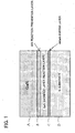
- FIG. 1 illustrates a schematic cross-sectional view which explains a basic idea of a method for producing a semiconductor crystal in the present invention.
- a reaction prevention layer is formed to prevent Si from reacting with a gallium nitride group semiconductor (semiconductor crystal A) which is deposited after the reaction prevention layer is formed.
- reaction prevention layer comprising a material whose melting point or thermal stability is higher than that of a gallium nitride group semiconductor, e.g., SiC and AlN, on the sacrifice layer, a reaction part described above is not formed in the semiconductor substrate (semiconductor crystal A) deposited on the reaction prevention layer when the gallium nitride group semiconductor (semiconductor crystal A) is grown by crystal growth for a long time.
- the reaction prevention layer prevents silicon (Si) from diffusing, the reaction part is generated only in the sacrifice layer and it is never formed at the upper portion of the reaction prevention layer even by growing the semiconductor crystal A at a high temperature for a long time.
- a semiconductor layer comprising a polycrystalline GaN high temperature reaction part made of polycrystalline lump
- stress which acts to the reaction prevention layer is relaxed and hardly functions so as to form a crack on the reaction prevention layer.
- cracks which penetrate the reaction prevention layer in longitudinal direction are hardly generated.
- the base substrate (Si substrate) and the gallium nitride group semiconductor (semiconductor crystal A) can be completely interrupted by the reaction prevention layer having no cracks which penetrate in longitudinal direction, generation of the above-described reaction part in the semiconductor substrate (semiconductor crystal A) can be prevented more securely.
- the reaction part described above is made of polycrystalline lump of GaN, the reaction part is structurally weak and fragile, and has a small endurance toward external force and inner stress. Accordingly, an objective semiconductor substrate can be easily separated from the base substrate (Si substrate) at the sacrifice layer comprising the reaction part.
- the second aspect is drawn to a method of the first aspect, wherein the semiconductor crystal A comprises a group III nitride compound semiconductor having a composition of Al x Ga y In (1-x-y) N (0 ⁇ x ⁇ 0.9, 0.1 ⁇ y ⁇ 1, 0 ⁇ x+y ⁇ 1).
- the third aspect is drawn to a method of the first or second aspect, wherein at least one of silicon carbide (SiC), aluminum nitride (AlN), and spinel (MgAl 2 O 4 ) is used as monocrystalline material B forming the reaction prevention layer.
- SiC silicon carbide
- AlN aluminum nitride
- MgAl 2 O 4 spinel
- the fourth aspect is drawn to a method of the first or second aspect, wherein AlGaN, AlInN, or AlGaInN, in which aluminum composition ratio is at least 0.30 or more, is used as monocrystalline material B forming the reaction prevention layer.
- a material having comparatively strong interatomic binding energy, high thermal stability (fusing point) and high stability may be preferably employed as monocrystalline material B.
- the fifth aspect is drawn to a method according to any one of the first to fourth aspects, wherein thickness of the reaction prevention layer is in a range of 0.1 ⁇ m to 2 ⁇ m. More preferably, thickness of the reaction prevention layer is in a range of 0.5 ⁇ m to 1.5 ⁇ m.
- each reaction prevention layer When the thickness of each reaction prevention layer is too small, because the thickness is not uniform and the monocrystalline material B is not a material with sufficient stability, gallium (Ga) or gallium nitride (GaN) and silicon (Si) cannot be completely interrupted. As a result, formation of reaction part (poly-crystalline GaN) may not be prevented sufficiently.
- each reaction prevention layer When the thickness of each reaction prevention layer is too large, cracks tends to be generated in the reaction prevention layer, and gallium (Ga) or gallium nitride (GaN) and silicon (Si) in the semiconductor crystal A (semiconductor substrate) formed thereon cannot be completely interrupted. As a result, formation of reaction part may not be prevented sufficiently, to thereby generate the reaction part in the semiconductor substrate (the upper layer semiconductor crystal A).
- each reaction prevention layer When the thickness of each reaction prevention layer is too large, more time and materials are needed to deposit the reaction prevention layer, to thereby unfavorably increase the production cost of the device.
- the sixth aspect is drawn to a method according to any one of the first to fifth aspects, wherein two or more reaction prevention layers are deposited.
- two or more reaction prevention layers are deposited.
- the seventh aspect is drawn to a method according to any one of the first to sixth aspects, wherein a buffer layer C made of Al x Ga 1-x N (0 ⁇ x ⁇ 1) is formed directly on the base substrate or the reaction prevention layer.
- the buffer layer C is a semiconductor layer made of AlN or AlGaN which grows at the temperature around 1100°C.
- a middle layer (it may be called just “a buffer layer” hereinafter) having almost the same compositions as those of the buffer layer C (e.g., AlN and AlGaN) may be further formed in the semiconductor substrate (semiconductor crystal A) periodically, alternatively with other layers, or deposited so that the middle layer has a multiple layer structure.
- the monocrystalline material B constructing the reaction prevention layer is such as silicon carbide (SiC).
- SiC silicon carbide
- the eighth aspect is drawn to a method according to the seventh aspect, wherein two or more buffer layers C are laminated.
- two buffer layers C are formed in total on each upper surface of the base substrate (Si substrate) and the reaction prevention layer.
- the ninth aspect is drawn to a method according to the seventh or eighth aspect, wherein the buffer layer C is formed to have thickness of 0.01 ⁇ m to 1 ⁇ m. More preferably, thickness of the buffer layer C is in a range of 0.02 ⁇ m to 0.5 ⁇ m.
- the buffer layer C When thickness of the buffer layer C is too large, cracks tend to be generated in the buffer layer and more production time and materials are needed. That is not favorable to the production cost of the device.
- the buffer layer C When the buffer layer C is too thin, it becomes difficult to form the buffer layer to have almost uniform thickness. As a result, the buffer layer becomes to have ununiform thickness (or a portion where it is not grown adequately), crystallinity of the buffer layer tends to be ununiform, and that is not desirable.
- the tenth aspect is drawn to a crystal growing process according to any one of the first to ninth aspects, wherein the semiconductor crystal A is deposited to have a thickness of 50 ⁇ m or more.
- the larger thickness of the semiconductor crystal A is, the more tensile stress to the semiconductor substrate (semiconductor crystal A) is relaxed. That decreases generation of dislocations and cracks in the semiconductor substrate and at the same time strengthen the semiconductor substrate. As a result, it becomes easier to handle it as a semiconductor substrate.
- the eleventh aspect is drawn to a group III nitride compound semiconductor device comprising the semiconductor crystal which is formed by the method of any one of the first to tenth aspects as a crystal growth substrate.
- a group III nitride compound semiconductor device e.g., a light-emiting device such as an LED or a transistor circuit such as an FET, made of a semiconductor which has excellent crystallinity and less inner stress can be obtained or easily produced.
- the twelfth aspect is to form a group III nitride compound semiconductor device by employing crystal growth in which a semiconductor crystal manufactured by the method of any one of the first to tenth aspects functions as a crystal growth substrate.
- the thirteenth aspect of the present invention provides a method for producing a semiconductor substrate in which a semiconductor crystal A comprising a Group III nitride compound semiconductor is grown on a base substrate comprising silicon (Si), comprising the steps of: a thin film part forming process in which a thin film part comprising silicon (Si) is formed as a crystal growth front of the base substrate by forming a cavity right under the crystal growth front of the base substrate; a reaction prevention layer forming process in which a reaction prevention layer made of a monocrystalline material B whose melting point or thermal stability is higher than that of the semiconductor crystal A is deposited on the thin film part; and a crystal growing process for growing the semiconductor crystal A on the reaction prevention layer by crystal growth.
- a thin film part forming process in which a thin film part comprising silicon (Si) is formed as a crystal growth front of the base substrate by forming a cavity right under the crystal growth front of the base substrate
- a reaction prevention layer forming process in which a reaction prevention layer made of a monocrystalline material
- the semiconductor substrate comprising the semiconductor crystal A may have a single layer structure. Alternatively, it may also have a multiple layer structure.
- group III nitride compound semiconductor generally refers to a binary, ternary, or quaternary semiconductor having arbitrary compound crystal proportions and represented by Al x Ga y In (1-x-y) N (0 ⁇ x ⁇ 1, 0 ⁇ y ⁇ 1, 0 ⁇ x+y ⁇ 1).
- a semiconductor doped with p-type or n-type impurity is also included in a group III nitride compound semiconductor described in the present specification.
- Group III elements Al, Ga, In
- B boron
- Tl thallium
- N nitrogen
- P phosphorus
- Au arsenic
- Sb antimony
- Bi bismuth
- Such a semiconductor may also be included in "a group III nitride compound semiconductor" in the present specification.
- Examples of the aforementioned p-type impurity include magnesium (Mg) and calcium (Ca).
- n-type impurity examples include silicon (Si), sulfur (S), selenium (Se), tellurium (Te), and germanium (Ge).
- impurities may be incorporated in combination of two or more species, and a p-type impurity and an n-type impurity may be incorporated in combination.
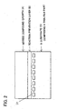
- FIG. 2 illustrates a schematic cross-sectional view which explains a basic idea of a method for producing a semiconductor crystal in the present invention.
- a reaction prevention layer is formed to prevent Si from reacting with a gallium nitride group semiconductor (semiconductor crystal A).
- a reaction prevention layer comprising a material whose melting point or thermal stability is higher than that of a gallium nitride group semiconductor (semiconductor crystal A), e.g., SiC and AlN
- a reaction part described above is not formed around silicon interface when the gallium nitride group semiconductor (semiconductor crystal A) is grown by crystal growth for a long time.
- the fourteenth aspect is drawn to a method of the thirteenth aspect, wherein the semiconductor crystal A comprises a group III nitride compound semiconductor having a composition of Al x Ga y In (1-x-y) N (0 ⁇ x ⁇ 1, 0 ⁇ y ⁇ 1, 0 ⁇ x+y ⁇ 1).
- the fifteenth aspect is drawn to a method of the thirteenth or fourteenth aspect, wherein at least one of silicon carbide (SiC), aluminum nitride (AlN), and spinel (MgAl 2 O 4 ) is used as monocrystalline material B forming the reaction prevention layer.
- SiC silicon carbide
- AlN aluminum nitride
- MgAl 2 O 4 spinel
- the sixteenth aspect is drawn to a method of the thirteenth or fourteenth aspect, wherein AlGaN, AlInN, or AlGaInN, in which aluminum composition ratio is at least 0.30 or more, is used as monocrystalline material B forming the reaction prevention layer.
- a material having comparatively strong interatomic binding energy, high thermal stability (fusing point) and high stability may be preferably employed as monocrystalline material B.
- the seventeenth aspect is drawn to a method according to any one of the thirteenth to sixteenth aspects, wherein thickness of the reaction prevention layer is in a range of 0.1 ⁇ m to 2 ⁇ m.
- each reaction prevention layer When the thickness of each reaction prevention layer is too small, because the thickness is not uniform and the monocrystalline material B is not a material with sufficient stability, gallium (Ga) or gallium nitride (GaN) and silicon (Si) cannot be completely interrupted. As a result, formation of reaction part (poly-crystalline GaN) may not be prevented sufficiently.
- reaction prevention layer When thickness of each reaction prevention layer is too large, cracks tends to be generated in the reaction prevention layer, and gallium (Ga) or gallium nitride (GaN) and silicon (Si) cannot be completely interrupted. As a result, formation of reaction part may not be prevented sufficiently.
- each reaction prevention layer When the thickness of each reaction prevention layer is too large, more time and materials are needed to deposit the reaction prevention layer, to thereby unfavorably increase the production cost of the device.
- the eighteenth aspect is drawn to a reaction prevention layer forming process according to any one of the thirteenth to seventeenth aspects, wherein a buffer layer C made of Al x Ga 1-x N (0 ⁇ x ⁇ 1) is formed on the reaction prevention layer after said reaction prevention layer forming process.
- the buffer layer C is a semiconductor layer made of AlN or AlGaN which grows at the temperature around 1100°C.
- a middle layer (it may be called just “a buffer layer” hereinafter) having almost the same compositions as those of the buffer layer C (e.g., AlN and AlGaN) may be further formed in the semiconductor substrate (semiconductor crystal A) periodically, alternatively with other layers, or deposited so that the middle layer has a multiple layer structure.
- the monocrystalline material B constructing the reaction prevention layer is such as silicon carbide (SiC).
- SiC silicon carbide
- the nineteenth aspect is drawn to a method according to the eighteenth aspect, wherein the buffer layer C is formed to have thickness of 0.01 ⁇ m to 1 ⁇ m. More preferably, thickness of the buffer layer C is in a range of 0.02 ⁇ m to 0.5 ⁇ m.
- the buffer layer C When thickness of the buffer layer C is too large, cracks tend to be generated in the buffer layer C and more production time and materials are needed. That is not favorable to the production cost of the device.
- the buffer layer C When the buffer layer C is too thin, it becomes difficult to form the buffer layer to have almost uniform thickness. As a result, the buffer layer becomes to have ununiform thickness (or a portion where it is not grown properly), crystallinity of the buffer layer tends to be ununiform, and that is not desirable.
- the twentieth aspect is drawn to a method according to any one of the thirteenth to nineteenth aspects, further comprising a separation process for separating the semiconductor crystal A and the base substrate, wherein stress owing to differences of thermal expansion coefficients is generated by cooling or heating the substrate crystal A and the base substrate, and sidewalls of the cavities are broken by using the stress.
- the semiconductor substrate semiconductor crystal A
- inner stress or outer stress becomes easy to act intensively to the sidewalls of the cavities.
- especially these stress function as shearing stress toward the sidewalls of cavities.
- the shearing stress becomes larger, the thin film part ruptures.
- the base substrate and the semiconductor substrate can be easily separated by applying the stress.
- the semiconductor crystal A and the base substrate can be easily separated because it becomes easy to generate stress.
- a part of the base substrate e.g., rupture remains of the thin film part or sidewalls of the cavity
- this separation process does not necessarily require complete or perfect separation of each material with no remains.
- Such rupture remains may be removed by using conventional methods such as wrapping and etching if necessary.
- the twenty-first aspect is drawn to the crystal growing process according to any one of the thirteenth to twentieth aspects, wherein the semiconductor crystal A is deposited to have a thickness of 50 ⁇ m or more.
- the larger thickness of the semiconductor crystal A is, the more tensile stress to the semiconductor substrate (semiconductor crystal A) is relaxed. That decreases generation of dislocations and cracks in the semiconductor substrate and at the same time strengthen the semiconductor substrate. As a result, it becomes easier to concentrate the stress to sidewalls of the cavity.
- thickness of the thin film part is 20 ⁇ m or less.
- the thinner this thickness is, the more the tensile stress to the semiconductor substrate (semiconductor crystal A) is relaxed. That results in decreasing generation of dislocations and cracks in the semiconductor substrate.
- the thin film part may preferably have thickness in a range of 0.02 ⁇ m to 20 ⁇ m.
- thickness of an objective semiconductor crystal which is formed by crystal growth is approximately the same or larger than that of the thin film part.
- This stress relaxing effect grows larger according to that thickness of the objective semiconductor crystal growth relatively thicker. Although it depends on conditions such as thickness of the thin film part, this stress relaxing effect is almost saturated with about 50 ⁇ m to 200 ⁇ m of the objective grown semiconductor crystal when thickness of the thin film part is 20 ⁇ m or less.
- the twenty-second aspect is drawn to a thin film part forming process according to any one of the thirteenth to twenty-first aspects, further comprising a concave part forming process in which a cavity whose top is opened is formed in silicon crystal comprising the base substrate through physical or chemical etching treatment is carried out and then a cavity and the thin-film part are formed by migration function around the surface of the substrate owing to heat treatment at a temperature of 1000°C to 1350°C.
- the twenty-third aspect is drawn to a thin film part forming process according to any one of the thirteenth to twenty-first aspects, the thin film part forming process comprising: an ion injecting process in which ion is injected into the silicon crystal forming the thin film part; a concave part forming process in which a cavity whose top is opened is formed in the silicon crystal comprising the base substrate except for the thin film part through physical or chemical etching treatment; a junction process in which the thin film part is joined to the cavity part through heat treatment; and an exfoliating process in which the thin film part is exfoliated at an ion injection part functioning as a separation front.
- At least the thin film part forming process in the present invention can be or is easily carried out adequately and concretely according to the twenty-second and twenty-third aspects.
- the thin film part forming process in the present invention is not necessarily limited thereto, but it may be carried out by employing appropriate method. That is, actions and effects of the present invention may be obtained properly or more than that by employing such method.
- the twenty-fourth aspect is drawn to a thin film part forming process according to any one of the thirteenth to twenty-third aspects, wherein height of the cavity is 0.1 ⁇ m to 10 ⁇ m. More preferably, height of the cavity may be 0.5 ⁇ m to 5 ⁇ m.
- the twenty-fifth aspect is drawn to a group III nitride compound semiconductor device comprising the semiconductor crystal which is formed by the method of any one of the thirteenth to twenty-fourth aspects as a crystal growth substrate.
- a group III nitride compound semiconductor device made of a semiconductor which has excellent crystallinity and less inner stress can be obtained or easily produced.
- the twenty-sixth aspect is to form a group III nitride compound semiconductor device by employing crystal growth in which a semiconductor crystal manufactured by the method of any one of the thirteenth to twenty-fourth aspects functions as a crystal growth substrate.
- each producing condition may be chosen from the followings. Also each producing condition may be combined arbitrary with each other.
- Group III nitride compound semiconductor layers are preferably formed through metal-organic vapor phase growth (MOCVD or MOVPE).
- MOCVD metal-organic vapor phase growth
- Other growth methods such as molecular-beam epitaxy (MBE), halide vapor phase growth (halide VPE), and liquid phase growth (LPE), may also be employed.
- MBE molecular-beam epitaxy
- halide VPE halide vapor phase growth
- LPE liquid phase growth
- the respective layers may be formed through different methods.
- a buffer layer is appropriately provided in the crystal growth substrate or formed on such as the base substrate, for several reasons, such as compensation of lattice mismatch.
- the buffer layer is preferably formed from a Group III nitride compound semiconductor Al x Ga y In 1-x-y N (0 ⁇ x ⁇ 1; 0 ⁇ y ⁇ 1; 0 ⁇ x+y ⁇ 1) which is formed at low temperature, more preferably Al x Ga 1-x N (0 ⁇ x ⁇ 1).
- the buffer layer may be a single layer or a multi-layer comprising a plurality of sub layers of different compositions.
- the buffer layer may be formed at a low temperature (380-420°C), or may be formed at 1000-1180°C through MOCVD.
- a buffer layer comprising AlN may be formed through reactive sputtering by use of a DC magnetron sputtering apparatus, from high-purity metallic aluminum and nitrogen gas serving as raw materials.
- the buffer layer comprising a compound semiconductor represented by formula Al x Ga y In 1-x-y N (0 ⁇ x ⁇ 1; 0 ⁇ y ⁇ 1; 0 ⁇ x+y ⁇ 1; arbitrary compositional proportions) can be formed through physical vapor deposition such as vapor deposition, ion plating, laser ablation, or ECR.
- the buffer layer is preferably formed through physical vapor deposition at 200-600°C, more preferably 300-600°C, most preferably 350-450°C.
- the buffer layer which is formed through physical vapor deposition such as sputtering preferably has a thickness of 100-3,000 ⁇ , more preferably 100-400 ⁇ , most preferably 100-300 ⁇ .
- a buffer layer of multi-layer type is formed through any of several methods. For example, an Al x Ga 1-x N (0 ⁇ x ⁇ 1) layer and a GaN layer are alternately formed, or a semiconductor layer of the same composition is alternately formed at different temperatures, such as 600°C or lower and 1000°C or higher. These two methods may be employed in combination.
- the multi-layer buffer layer may be formed by stacking at least three species selected from Group III nitride compound semiconductors represented by Al x Ga y In 1-x-y N (0 ⁇ x ⁇ 1; 0 ⁇ y ⁇ 1; 0 ⁇ x+y ⁇ 1). Generally, a buffer layer is made of non-crystal and an intermediate layer is made of monocrystalline. Repetitions of unit of a buffer layer and an intermediate layer may be formed, and the number of repetitions is not particularly limited. The larger the number of repetitions are, the greater the improvement in crystallinity becomes.
- the present invention is substantially applicable even when the composition of a buffer layer and that of a Group III nitride compound semiconductor formed on the buffer layer are such that a portion of Group III elements are replaced with boron (B) or thallium (Tl) or a portion of nitrogen (N) atoms are replaced with phosphorus (P), arsenic (As), antimony (Sb), or bismuth (Bi). Also, the buffer layer and the Group III nitride compound semiconductor may be doped with any one of these elements to such an extent as not to appear in the composition thereof.
- a Group III nitride compound semiconductor which is represented by Al x Ga 1- x N (0 ⁇ x ⁇ 1) and which does not contain indium (In) and arsenic (As) may be doped with indium (In), which is larger in atomic radius than aluminum (Al) and gallium (Ga), or arsenic (As), which is larger in atomic radius than nitrogen (N), to thereby improve crystallinity through compensation, by means of compression strain, for crystalline expansion strain induced by dropping off of nitrogen atoms.
- the Group III nitride compound semiconductor layers are further preferably doped with an element greater in atomic radius than a predominant component element.
- a binary or ternary Group III nitride compound semiconductor is preferred.
- n-type Group III nitride compound semiconductor layer When an n-type Group III nitride compound semiconductor layer is to be formed, a Group IV or Group VI element, such as Si, Ge, Se, Te, or C, can be added as an n-type impurity.
- a Group II or Group IV element such as Zn, Mg, Be, Ca, Sr, or Ba, can be added as a p-type impurity.
- the same layer may be doped with a plurality of n-type or p-type impurities or doped with both n-type and p-type impurities.
- Dislocations occurring in a Group III nitride compound semiconductor layer can also be reduced through employment of lateral epitaxial growth.
- lateral epitaxial growth can be performed in an arbitrary manner; e.g., by use of a mask or through employment of etching for leveling a step and supplying the step as seed for executing ELO between steps.
- the aforementioned etching mask may be formed from a polycrystalline semiconductor such as polycrystalline silicon or polycrystalline nitride semiconductor; an oxide or nitride such as silicon oxide (SiO x ), silicon nitride (SiN x ), titanium oxide (TiO x ), or zirconium oxide (ZrO x ); or a high-melting-point metal such as titanium (Ti) or tungsten (W).
- a multi-layer film of these materials may also be employed.
- the film can be formed through any film formation method such as vapor phase growth (e.g., vapor deposition, sputtering, or CVD).
- a step having a surface of a side wall which is not normal to the substrate plane may be formed.
- a step which does not have a flat surface on the bottom of the substrate and which has a V-shape cross-section may be formed through anisotropic etching.
- a semiconductor device such as an FET or a light-emitting device, can be formed on the aforementioned Group III nitride compound semiconductor.
- a light-emitting layer may have a multi-quantum well (MQW) structure, or a single-quantum well (SQW) structure, and the device may have a homo-structure, a single-hetero-structure, or a double-hetero-structure, or the layer may be formed by means of, for example, a pin junction or a pn junction.
- MQW multi-quantum well
- SQW single-quantum well
- Al x Ga 1-x N (x ⁇ 0.20) buffer layer C is formed at a temperature of about 1100°C through metal organic vapor phase epitaxy (MOVPE) on a Si(111) substrate.
- MOVPE metal organic vapor phase epitaxy
- MOVPE vapor phase growth
- reaction prevention layer forming process a reaction prevention layer is deposited on the above described sacrifice layer.
- AlN aluminum nitride
- MOVPE vapor phase growth
- a semiconductor crystal A (GaN) is grown on the reaction prevention layer B to have thickness of about 200 ⁇ m through halide vapor phase growth (HVPE).
- GaN layer semiconductor crystal A
- HVPE halide vapor phase growth
- this removing process may be carried out through etching treatment using a mixture of hydrofluoric acid and nitric acid.
- the reaction prevention layer B may not be removed. For example, whether to carry out the remains removing process or not can be selected according to conditions such as the structure of electrode connection of the light-emitting semiconductor device.
- GaN layer 102b a GaN crystal having thickness of about 200 ⁇ m and excellent crystallinity, which is a desired free-standing semiconductor substrate independent from the base substrate 101, was obtained through the method described above.
- GaN gallium nitride
- a semiconductor light-emitting device e.g., to a crystal growth substrate
- a semiconductor product e.g., a semiconductor light-emitting device and a semiconductor light-receiving device, which has a high luminous efficiency and whose driving voltage is more decreased compared with a conventional device.
- a buffer layer forming process in which crystal growth is carried out at a high temperature of 1000°C to 1180°C may be further employed between the reaction prevention layer forming process and the crystal growth process.
- materials such as Al x Ga 1-x N (0 ⁇ x ⁇ 1) may be used as monocrystalline material B for forming the reaction prevention layer. Approximately same action and effect as in this embodiment may be obtained by employing such monocrystalline material B.
- silicon carbide SiC
- aluminum nitride AlN
- spinel MgAl 2 O 4
- AlGaN, AlInN and AlGaInN whose aluminum composition ratio is at least 0.30 and more may be used as monocrystalline material B for forming the reaction prevention layer.
- the semiconductor crystal A which forms an objective semiconductor substrate is not limited to gallium nitride (GaN) but may be selected from the above-mentioned group III nitride compound semiconductor.
- the objective semiconductor substrate (semiconductor crystal A) may have a multiple layer structure.
- growth temperature of the semiconductor crystal A constituting the objective semiconductor substrate may be raised in halfway of its growing process and a semiconductor layer grown at higher temperature may be formed at the upper portion (upper layer).
- the same action and effect as in the present invention may be obtained by forming the semiconductor layer having multiple layer structure or by forming a middle layer such as a buffer layer in the multiple layer structure.
- materials of "a sacrifice layer” may not be necessarily the same as those of the objective semiconductor substrate (semiconductor crystal A).
- the materials of "a sacrifice layer” may also be arbitrary selected among the above-mentioned general "Group III nitride compound semiconductor.”
- kinds (materials) of the sacrifice layer and the objective semiconductor crystal are not particularly limited in the present invention, and the present invention can be applied to well-known or arbitrary kind of hetero-epitaxial growth on the base substrate (Si substrate) described above.
- MOVPE metal-organic vapor phase epitaxly
- HVPE halide vapor phase growth
- the semiconductor crystal A is employed as a crystal growth substrate of the semiconductor device after separating the base substrate and removing the remains.
- processes of separating the base substrate and removing the remains may be carried out after depositing the semiconductor layer of the semiconductor device.
- the semiconductor crystal A may be used as a semiconductor device without particularly carrying out the separating process and the remains removing process.
- a concave part forming process in which a cavity whose top is opened is formed in silicon crystal as a base substrate through physical or chemical etching treatment is carried out and then a cavity and a thin-film part are formed by migration function around the surface of the substrate owing to heat treatment at a temperature of 1000°C to 1200°C.
- a reaction prevention layer forming process is a process for depositing a reaction prevention layer on a base substrate (Si substrate D) which comprises the thin-film part D1.
- a reaction prevention layer B made of aluminum nitride (AlN) is formed at a temperature of about 1100°C on the crystal growth plane (thin-film part D1) of the Si (111) substrate through metal organic chemical vapor deposition (MOCVD).
- a semiconductor crystal A (GaN) is grown on the surface of the reaction prevention layer B to have a thickness of about 200 ⁇ m through metal-organic vapor phase epitaxy (hereinafter called "MOVPE").
- MOVPE metal-organic vapor phase epitaxy
- ammonia NH 3
- carrier gas H 2 or N 2
- trimethylgallium Ga(CH 3 ) 3
- TMG trimethylgallium
- Al(CH 3 ) 3 Al(CH 3 ) 3
- a GaN layer (semiconductor crystal A) is grown on the reaction prevention layer B by crystal growth through MOVPE treatment until its thickness becomes 200 ⁇ m. Crystal growth velocity of the GaN layer though MOVPE is about 30 ⁇ m/Hr.
- this removing process may be carried out through etching treatment using a mixture of hydrofluoric acid and nitric acid. And the reaction prevention layer B may be also removed.
- GaN layer having a thickness of about 200 ⁇ m and excellent crystallinity, which is an objective free-standing semiconductor substrate (semiconductor crystal A) independent from the base substrate, was obtained through the method described above.
- GaN gallium nitride
- a semiconductor light-emitting device e.g., to a crystal growth substrate
- a semiconductor product e.g., a semiconductor light-emitting device and a semiconductor light-receiving device, which has a high luminous efficiency and whose driving voltage is more decreased compared with a conventional device.
- a buffer layer forming process in which crystal growth is carried out at a high temperature of 1000°C to 1180°C may be further employed between the reaction prevention layer forming process and the crystal growth process.
- the thin-film part of the base substrate is obtained by forming a lot of cavities near the crystal growth plane of the base substrate as shown in FIG. 2.
- the cavities may be formed in sequence.
- the cavity may be formed, for example, such that one long and narrow tubular tunnel is formed elaborately in a scroll shape.
- FIG. 2 of this case can be interpreted as a sectional view of the base substrate comprising such a cavity.
- the conditions of a cavity which is objected to form the thin film part of the base substrate are generally arbitral.
- the thin film part forming process in the second embodiment is replaced with "thin film part forming process" described below. With respect to other processes, the same processes as in the second embodiment may be carried out.
- This process is for forming a cavity and a thin film part, comprising an ion injection process in which ion is injected into a silicon crystal providing a thin film part, a concave part forming process in which a cavity whose top is opened is formed in the silicon crystal constituting the base substrate except for the thin film part through physical or chemical etching treatment, a junction process in which the thin film part is joined to the cavity part through heat treatment, and an exfoliating process in which the thin film part is exfoliated at an ion injection part functioning as a separation front.
- He + helium ion
- H + hydrogen ion
- Doping amount of hydrogen ion may be, although it depends on a material used to form the base layer, about 1 x 10 15 [cm 2 ] to 1 x 10 20 [cm 2 ] to obtain approximately the same action and effect as those of the above embodiment. More preferably, doping amount of hydrogen ion may be about 3 x 10 15 [/cm 2 ] to 1 x 10 17 [/cm 2 ], and further preferably, it may be about 8 x 10 15 [/cm 2 ] to 2 x 10 16 [/cm 2 ].
- the thickness of the thin film part separated from the base substrate can be controlled by varying the incident energy.
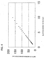
- FIG. 4 illustrates the result of measuring depth (depth h at the maximum ion concentration) of injecting ion toward injection energy of ion. Accordingly, for example, because the depth of ion injection (depth h at the maximum ion concentration) is approximately in proportion to injection energy of ion, the thickness of the thin film part may be controlled properly by adjusting the amount of incident energy (accelerating voltage).
- a partial ruptured part (void) is formed at the ion injection layer in advance and crystallinity of the ion injection part of the base substrate, which is damaged by ion irradiation, can be recovered.
- Thickness of the thin film part D1 may preferably 20 ⁇ m or less.
- the thinner then thin film part is, the more tensile stress toward the objective grown semiconductor crystal is relaxed, and that can decrease generation of dislocations or cracks in the objective grown semiconductor crystal.
- thickness of the thin film part may be 2 ⁇ m or less, and further preferably, 200nm or less.
- ion injection energy accelerating voltage
- ion injection energy may be controlled in accordance with the graph in FIG. 4 so that the depth when the numbers of injected ion becomes its peak corresponds to the desired thickness of the thin film part.
- thickness of the ion injection layer cannot be strictly defined, the full width half maximum in the characteristics of the numbers of injected ion in FIG. 3, for example, may be used as one standard.
- materials such as Al x Ga 1-x N (0 ⁇ x ⁇ 1) may be used as monocrystalline material B for forming the reaction prevention layer to obtain approximately same action and effect as in the above embodiments.
- silicon carbide (SiC), aluminum nitride (AlN), spinel (MgAl 2 O 4 ), or AlGaN, AlInN and AlGaInN whose aluminum composition ratio is at least 0.30 and more may be used as monocrystalline material B forming the reaction prevention layer.
- the semiconductor crystal A which forms an objective semiconductor substrate is not limited to gallium nitride (GaN) but may be selected from the above-mentioned group III nitride compound semiconductor.
- the objective semiconductor substrate (semiconductor crystal A) may have a multiple layer structure.
- kinds (materials) of the base substrate and the objective semiconductor crystal have no special limitation. So the present invention, including the above-described arbitrary combination of each material of the base substrate and the semiconductor crystal, can be applied to well-known and arbitral kind of hetero epitaxial growth.
- Metal-organic vapor phase epitaxly is employed in the above embodiment.
- crystal growth of the present invention may be carried out through halide vapor phase growth (HVPE).
- the semiconductor crystal A is employed as a crystal growth substrate of the semiconductor device after separating the base substrate and removing the remains.
- processes of separating the base substrate and removing the remains may be carried out after depositing the semiconductor layer of the semiconductor device.
- the semiconductor crystal A may be used as a semiconductor device without particularly carrying out the separating process and the remains removing process.
Landscapes
- Chemical & Material Sciences (AREA)
- General Chemical & Material Sciences (AREA)
- Chemical Kinetics & Catalysis (AREA)
- Engineering & Computer Science (AREA)
- Materials Engineering (AREA)
- Mechanical Engineering (AREA)
- Metallurgy (AREA)
- Organic Chemistry (AREA)
- Led Devices (AREA)
Abstract
A reaction prevention layer is formed to prevent Si
from reacting with a gallium nitride group semiconductor
(semiconductor crystal A) which is deposited after the
reaction prevention layer is formed. By forming a reaction
prevention layer comprising a material whose melting point or
thermal stability is higher than that of a gallium nitride
group semiconductor, e.g., AlN, on a sacrifice layer, a
reaction part is not formed in the semiconductor substrate
deposited on the reaction prevention layer when the gallium
nitride group semiconductor is grown by crystal growth for a
long time. In short, owing to the effect that the reaction
prevention layer prevents silicon (Si) from diffusing, the
reaction part is generated only in the sacrifice layer and it
is never formed at the upper portion of the reaction
prevention layer even by growing the semiconductor crystal A
at a high temperature for a long time.
Description
The present invention relates to a method for producing
a semiconductor substrate by growing a crystal of group III
nitride compound semiconductor on a base substrate comprising
silicon (Si). The present invention also relates to a
semiconductor device, e.g., a group III nitride compound
semiconductor device, formed on such a semiconductor
substrate obtained by above method.
FIG. 5 is a schematic cross-sectional view showing a
conventional semiconductor crystal formed on a Si substrate
(a base substrate) by crystal growth. MOCVD is applied in a
process of crystal growth of the semiconductor crystal. As
shown in FIG. 5, a semiconductor crystal (e.g. GaN crystal)
grown at a high temperature on a Si substrate (base
substrate) by using a conventional technique has a reaction
part, dislocations and cracks.
Dislocations and cracks are occurred because of stress
which is generated owing to difference of thermal expansion
coefficients and difference of lattice constants between
different kinds of materials. So when such a crystal growth
substrate is used for fabricating each kind of semiconductor
devices, the characteristics of the device is deteriorated.
When the base substrate consisting of silicon (Si)
except for the grown layer is removed so as to obtain a free-standing
substrate (crystal), the substrate cannot have
larger area (1cm2 and bigger) because of dislocations and
cracks described above.
At the temperature for crystal growth of an objective
semiconductor substrate (semiconductor crystal A), or around
1000°C to 1150°C, silicon (Si) and gallium nitride (GaN)
happen to react ("reaction part" in FIG. 5). As a result, it
is not easy to obtain a single crystalline GaN substrate by
applying a crystal growing process in a high temperature.
A method of using a silicon thin film, which hardly
generates stress described above, alone as a crystal growth
substrate in order to obtain monocrystalline GaN substrate is
reported. But such a thin film is easily destroyed and it is
not easy to handle the thin film directly before carrying out
crystal growth. Accordingly, it was difficult to manufacture
semiconductor substrates each having a larger area and to
obtain a higher yield rate of the semiconductor substrates by
employing such conventional methods.
The present invention has been accomplished in order to
overcome the aforementioned drawbacks. An object of the
present invention is to effectively produce a semiconductor
crystal of high quality having no crack or polycrystalline
lump (reaction part which reacts at a high temperature) by
using silicon (Si) which can be provided at comparatively low
cost as a base substrate. Other object of the present
invention is to produce semiconductor devices of high quality
which are formed by using a high-quality semiconductor
crystal as a crystal growth substrate.
The following means may be useful to overcome the
above-described drawbacks.
That is, the first aspect of the present invention
provides a method for producing a semiconductor substrate in
which a semiconductor crystal A comprising a Group III
nitride compound semiconductor is grown on a base substrate
comprising silicon (Si), comprising the steps of: a sacrifice
layer forming process in which a sacrifice layer comprising
approximately the same kind of semiconductor as the
semiconductor crystal A is formed on the base substrate by
crystal growth; a reaction prevention layer forming process
in which a reaction prevention layer made of a
monocrystalline material B whose melting point or thermal
stability is higher than that of the semiconductor crystal A
and preventing silicon (Si) from diffusing is deposited on
the sacrifice layer; and a crystal growth process for growing
a semiconductor substrate made of the semiconductor crystal A
on the reaction prevention layer by crystal growth.
Here, the semiconductor substrate comprising the
semiconductor crystal A may have a single layer structure.
Alternatively, it may also have a multiple layer structure.
As used herein, the term group III nitride compound
semiconductor generally refers to a binary, ternary, or
quaternary semiconductor having arbitrary compound crystal
proportions and represented by AlxGayIn(1-x-y)N (0≤x≤1, 0≤y≤1,
0≤x+y≤1). A semiconductor doped with p-type or n-type
impurity is also included in a group III nitride compound
semiconductor described in the present specification.
Group III elements (Al, Ga, In) may be partially
replaced with boron (B) or thallium (Tl), and nitrogen (N)
atoms may be completely or partially replaced with phosphorus
(P), arsenic (As), antimony (Sb), or bismuth (Bi). Such a
semiconductor may also be included in "a group III nitride
compound semiconductor" in the present specification.
Examples of the aforementioned p-type impurity include
magnesium (Mg) and calcium (Ca).
Examples of the aforementioned n-type impurity include
silicon (Si), sulfur (S), selenium (Se), tellurium (Te), and
germanium (Ge).
These impurities may be incorporated in combination of
two or more species, and a p-type impurity and an n-type
impurity may be incorporated in combination.
FIG. 1 illustrates a schematic cross-sectional view
which explains a basic idea of a method for producing a
semiconductor crystal in the present invention. A reaction
prevention layer is formed to prevent Si from reacting with a
gallium nitride group semiconductor (semiconductor crystal A)
which is deposited after the reaction prevention layer is
formed. By forming a reaction prevention layer
(monocrystalline material B) comprising a material whose
melting point or thermal stability is higher than that of a
gallium nitride group semiconductor, e.g., SiC and AlN, on
the sacrifice layer, a reaction part described above is not
formed in the semiconductor substrate (semiconductor crystal
A) deposited on the reaction prevention layer when the
gallium nitride group semiconductor (semiconductor crystal A)
is grown by crystal growth for a long time.
In short, owing to the effect that the reaction
prevention layer prevents silicon (Si) from diffusing, the
reaction part is generated only in the sacrifice layer and it
is never formed at the upper portion of the reaction
prevention layer even by growing the semiconductor crystal A
at a high temperature for a long time.
By generating the reaction part in the sacrifice layer
intentionally, a semiconductor layer comprising a
polycrystalline GaN (high temperature reaction part made of
polycrystalline lump) is formed between the silicon (Si
substrate) and the reaction prevention layer. As a result,
after the reaction part is formed, stress which acts to the
reaction prevention layer is relaxed and hardly functions so
as to form a crack on the reaction prevention layer. As a
result, cracks which penetrate the reaction prevention layer
in longitudinal direction are hardly generated. And because
the base substrate (Si substrate) and the gallium nitride
group semiconductor (semiconductor crystal A) can be
completely interrupted by the reaction prevention layer
having no cracks which penetrate in longitudinal direction,
generation of the above-described reaction part in the
semiconductor substrate (semiconductor crystal A) can be
prevented more securely.
Owing to the polycrystalline lump, stress caused
between the base substrate and the semiconductor substrate is
relaxed. That enables to decrease unnecessary stress which
acts to a growing semiconductor substrate when the
semiconductor substrate (objective semiconductor crystal A)
is grown by crystal growth, to thereby reduce generation of
dislocations and cracks.
Owing to the stress relaxing action described above,
dislocations hardly occurs in the gallium nitride group
semiconductor (semiconductor crystal A), and generation of
cracks can be remarkably reduced.
Further, because the reaction part described above is
made of polycrystalline lump of GaN, the reaction part is
structurally weak and fragile, and has a small endurance
toward external force and inner stress. Accordingly, an
objective semiconductor substrate can be easily separated
from the base substrate (Si substrate) at the sacrifice layer
comprising the reaction part.
According to those actions and their synergism, it
becomes possible or easier to obtain a semiconductor
substrate (semiconductor crystal A) of high quality whose
dislocation concentration is sufficiently controlled and
which does not have reaction part and cracks.
The second aspect is drawn to a method of the first
aspect, wherein the semiconductor crystal A comprises a group
III nitride compound semiconductor having a composition of
AlxGayIn(1-x-y)N (0≤x<0.9, 0.1<y≤1, 0<x+y≤1).
The third aspect is drawn to a method of the first or
second aspect, wherein at least one of silicon carbide (SiC),
aluminum nitride (AlN), and spinel (MgAl2O4) is used as
monocrystalline material B forming the reaction prevention
layer.
The fourth aspect is drawn to a method of the first or
second aspect, wherein AlGaN, AlInN, or AlGaInN, in which
aluminum composition ratio is at least 0.30 or more, is used
as monocrystalline material B forming the reaction prevention
layer.
Further, a material having comparatively strong
interatomic binding energy, high thermal stability (fusing
point) and high stability may be preferably employed as
monocrystalline material B.
The fifth aspect is drawn to a method according to any
one of the first to fourth aspects, wherein thickness of the
reaction prevention layer is in a range of 0.1µm to 2µm.
More preferably, thickness of the reaction prevention layer
is in a range of 0.5µm to 1.5µm.
When the thickness of each reaction prevention layer is
too small, because the thickness is not uniform and the monocrystalline
material B is not a material with sufficient
stability, gallium (Ga) or gallium nitride (GaN) and silicon
(Si) cannot be completely interrupted. As a result,
formation of reaction part (poly-crystalline GaN) may not be
prevented sufficiently.
When the thickness of each reaction prevention layer is
too large, cracks tends to be generated in the reaction
prevention layer, and gallium (Ga) or gallium nitride (GaN)
and silicon (Si) in the semiconductor crystal A
(semiconductor substrate) formed thereon cannot be completely
interrupted. As a result, formation of reaction part may not
be prevented sufficiently, to thereby generate the reaction
part in the semiconductor substrate (the upper layer
semiconductor crystal A).
When the thickness of each reaction prevention layer is
too large, more time and materials are needed to deposit the
reaction prevention layer, to thereby unfavorably increase
the production cost of the device.
The sixth aspect is drawn to a method according to any
one of the first to fifth aspects, wherein two or more
reaction prevention layers are deposited. By depositing
plural numbers of reaction prevention layers, diffusing of
silicon can be prevented more securely. As a result,
generation of reaction part can be prevented more securely.
The seventh aspect is drawn to a method according to
any one of the first to sixth aspects, wherein a buffer layer
C made of AlxGa1-xN (0<x≤1) is formed directly on the base
substrate or the reaction prevention layer.
Here the buffer layer C is a semiconductor layer made
of AlN or AlGaN which grows at the temperature around 1100°C.
Alternatively, aside from the buffer layer C, a middle layer
(it may be called just "a buffer layer" hereinafter) having
almost the same compositions as those of the buffer layer C
(e.g., AlN and AlGaN) may be further formed in the
semiconductor substrate (semiconductor crystal A)
periodically, alternatively with other layers, or deposited
so that the middle layer has a multiple layer structure.
By depositing such a buffer layer (or a middle layer),
stress caused by difference of lattice constants and acting
to the semiconductor crystal A may be relaxed by the same
action principle as that of the conventional one. As a
result, crystallinity of the device is improved.
Such action and effect may be seen remarkable
especially when the monocrystalline material B constructing
the reaction prevention layer is such as silicon carbide
(SiC). In short, it is more preferable at this time to form
the buffer layer C on the reaction prevention layer.
The eighth aspect is drawn to a method according to the
seventh aspect, wherein two or more buffer layers C are
laminated. For example, two buffer layers C are formed in
total on each upper surface of the base substrate (Si
substrate) and the reaction prevention layer. By employing
multiple layer structure of the buffer layers, action and
effect as in the seventh aspect can be obtained more securely.
The ninth aspect is drawn to a method according to the
seventh or eighth aspect, wherein the buffer layer C is
formed to have thickness of 0.01 µm to 1µm. More preferably,
thickness of the buffer layer C is in a range of 0.02 µm to
0.5µm.
When thickness of the buffer layer C is too large,
cracks tend to be generated in the buffer layer and more
production time and materials are needed. That is not
favorable to the production cost of the device. When the
buffer layer C is too thin, it becomes difficult to form the
buffer layer to have almost uniform thickness. As a result,
the buffer layer becomes to have ununiform thickness (or a
portion where it is not grown adequately), crystallinity of
the buffer layer tends to be ununiform, and that is not
desirable.
The tenth aspect is drawn to a crystal growing process
according to any one of the first to ninth aspects, wherein
the semiconductor crystal A is deposited to have a thickness
of 50µm or more.
The larger thickness of the semiconductor crystal A is,
the more tensile stress to the semiconductor substrate
(semiconductor crystal A) is relaxed. That decreases
generation of dislocations and cracks in the semiconductor
substrate and at the same time strengthen the semiconductor
substrate. As a result, it becomes easier to handle it as a
semiconductor substrate.
The eleventh aspect is drawn to a group III nitride
compound semiconductor device comprising the semiconductor
crystal which is formed by the method of any one of the first
to tenth aspects as a crystal growth substrate.
Accordingly, a group III nitride compound semiconductor
device, e.g., a light-emiting device such as an LED or a
transistor circuit such as an FET, made of a semiconductor
which has excellent crystallinity and less inner stress can
be obtained or easily produced.
The twelfth aspect is to form a group III nitride
compound semiconductor device by employing crystal growth in
which a semiconductor crystal manufactured by the method of
any one of the first to tenth aspects functions as a crystal
growth substrate.
As a result, a group III nitride compound semiconductor
device made of a semiconductor which has excellent
crystallinity and less inner stress can be obtained or easily
manufactured.
Through employment of the aforementioned aspects of the
present invention, the aforementioned drawbacks can be
overcome effectively and rationally.
That is, the thirteenth aspect of the present invention
provides a method for producing a semiconductor substrate in
which a semiconductor crystal A comprising a Group III
nitride compound semiconductor is grown on a base substrate
comprising silicon (Si), comprising the steps of: a thin film
part forming process in which a thin film part comprising
silicon (Si) is formed as a crystal growth front of the base
substrate by forming a cavity right under the crystal growth
front of the base substrate; a reaction prevention layer
forming process in which a reaction prevention layer made of
a monocrystalline material B whose melting point or thermal
stability is higher than that of the semiconductor crystal A
is deposited on the thin film part; and a crystal growing
process for growing the semiconductor crystal A on the
reaction prevention layer by crystal growth.
Here, the semiconductor substrate comprising the
semiconductor crystal A may have a single layer structure.
Alternatively, it may also have a multiple layer structure.
As used herein, the term group III nitride compound
semiconductor generally refers to a binary, ternary, or
quaternary semiconductor having arbitrary compound crystal
proportions and represented by AlxGayIn(1-x-y)N (0≤x≤1, 0≤y≤1,
0≤x+y≤1). A semiconductor doped with p-type or n-type
impurity is also included in a group III nitride compound
semiconductor described in the present specification.
Group III elements (Al, Ga, In) may be partially
replaced with boron (B) or thallium (Tl), and nitrogen (N)
atoms may be completely or partially replaced with phosphorus
(P), arsenic (As), antimony (Sb), or bismuth (Bi). Such a
semiconductor may also be included in "a group III nitride
compound semiconductor" in the present specification.
Examples of the aforementioned p-type impurity include
magnesium (Mg) and calcium (Ca).
Examples of the aforementioned n-type impurity include
silicon (Si), sulfur (S), selenium (Se), tellurium (Te), and
germanium (Ge).
These impurities may be incorporated in combination of
two or more species, and a p-type impurity and an n-type
impurity may be incorporated in combination.
FIG. 2 illustrates a schematic cross-sectional view
which explains a basic idea of a method for producing a
semiconductor crystal in the present invention. A reaction
prevention layer is formed to prevent Si from reacting with a
gallium nitride group semiconductor (semiconductor crystal A).
By forming a reaction prevention layer (monocrystalline
material B) comprising a material whose melting point or
thermal stability is higher than that of a gallium nitride
group semiconductor (semiconductor crystal A), e.g., SiC and
AlN, on a base substrate (Si substrate), a reaction part
described above is not formed around silicon interface when
the gallium nitride group semiconductor (semiconductor
crystal A) is grown by crystal growth for a long time.
By forming a cavity, a thin film is formed at the side
of the crystal growth front of the silicon (Si substrate),
stress which acts to the reaction prevention layer is relaxed,
and hardly functions so as to form a crack on the reaction
prevention layer in longitudinal direction. As a result,
cracks which penetrate the reaction prevention layer in
longitudinal direction are hardly generated. And because the
base substrate (Si substrate) and the gallium nitride group
semiconductor (semiconductor crystal A) can be completely
interrupted by the reaction prevention layer having no cracks
which penetrate in longitudinal direction, generation of the
above-described reaction part can be prevented more securely.
Owing to the thin film part and the cavity, stress
caused by the difference of lattice constants of the base
substrate and the semiconductor substrate is relaxed. That
enables to decrease unnecessary stress which acts to a
growing semiconductor substrate when the semiconductor
substrate (objective semiconductor crystal A) grows by
crystal growth, to thereby reduce generation of dislocations
and cracks.
Owing to the stress relaxing action described above,
dislocations hardly occurs in the gallium nitride group
semiconductor (semiconductor crystal A), and generation of
cracks can be remarkably reduced.
According to those actions and their synergism, it
becomes possible or easier to obtain a semiconductor
substrate (semiconductor crystal A) of high quality whose
dislocation concentration is sufficiently suppressed and
which does not have reaction part and cracks.
The fourteenth aspect is drawn to a method of the
thirteenth aspect, wherein the semiconductor crystal A
comprises a group III nitride compound semiconductor having a
composition of AlxGayIn(1-x-y)N (0≤x<1, 0<y≤1, 0<x+y≤1).
The fifteenth aspect is drawn to a method of the
thirteenth or fourteenth aspect, wherein at least one of
silicon carbide (SiC), aluminum nitride (AlN), and spinel
(MgAl2O4) is used as monocrystalline material B forming the
reaction prevention layer.
The sixteenth aspect is drawn to a method of the
thirteenth or fourteenth aspect, wherein AlGaN, AlInN, or
AlGaInN, in which aluminum composition ratio is at least 0.30
or more, is used as monocrystalline material B forming the
reaction prevention layer.
Further, a material having comparatively strong
interatomic binding energy, high thermal stability (fusing
point) and high stability may be preferably employed as
monocrystalline material B.
The seventeenth aspect is drawn to a method according
to any one of the thirteenth to sixteenth aspects, wherein
thickness of the reaction prevention layer is in a range of
0.1µm to 2µm.
When the thickness of each reaction prevention layer is
too small, because the thickness is not uniform and the monocrystalline
material B is not a material with sufficient
stability, gallium (Ga) or gallium nitride (GaN) and silicon
(Si) cannot be completely interrupted. As a result,
formation of reaction part (poly-crystalline GaN) may not be
prevented sufficiently.
When thickness of each reaction prevention layer is too
large, cracks tends to be generated in the reaction
prevention layer, and gallium (Ga) or gallium nitride (GaN)
and silicon (Si) cannot be completely interrupted. As a
result, formation of reaction part may not be prevented
sufficiently.
When the thickness of each reaction prevention layer is
too large, more time and materials are needed to deposit the
reaction prevention layer, to thereby unfavorably increase
the production cost of the device.
The eighteenth aspect is drawn to a reaction prevention
layer forming process according to any one of the thirteenth
to seventeenth aspects, wherein a buffer layer C made of
AlxGa1-xN (0<x≤1) is formed on the reaction prevention layer
after said reaction prevention layer forming process.
Here the buffer layer C is a semiconductor layer made
of AlN or AlGaN which grows at the temperature around 1100°C.
Alternatively, aside from the buffer layer C, a middle layer
(it may be called just "a buffer layer" hereinafter) having
almost the same compositions as those of the buffer layer C
(e.g., AlN and AlGaN) may be further formed in the
semiconductor substrate (semiconductor crystal A)
periodically, alternatively with other layers, or deposited
so that the middle layer has a multiple layer structure.
By depositing such a buffer layer (or a middle layer),
stress caused by difference of lattice constants and acting
to the semiconductor crystal A may be relaxed by the same
action principle as that of the conventional one. As a
result, crystallinity of the device is improved.
Such action and effect may be seen remarkable
especially when the monocrystalline material B constructing
the reaction prevention layer is such as silicon carbide
(SiC). In short, it is more preferable at this time to form
the buffer layer C on the reaction prevention layer.
The nineteenth aspect is drawn to a method according to
the eighteenth aspect, wherein the buffer layer C is formed
to have thickness of 0.01 µm to 1µm. More preferably,
thickness of the buffer layer C is in a range of 0.02 µm to
0.5µm.
When thickness of the buffer layer C is too large,
cracks tend to be generated in the buffer layer C and more
production time and materials are needed. That is not
favorable to the production cost of the device. When the
buffer layer C is too thin, it becomes difficult to form the
buffer layer to have almost uniform thickness. As a result,
the buffer layer becomes to have ununiform thickness (or a
portion where it is not grown properly), crystallinity of the
buffer layer tends to be ununiform, and that is not desirable.
The twentieth aspect is drawn to a method according to
any one of the thirteenth to nineteenth aspects, further
comprising a separation process for separating the
semiconductor crystal A and the base substrate, wherein
stress owing to differences of thermal expansion coefficients
is generated by cooling or heating the substrate crystal A
and the base substrate, and sidewalls of the cavities are
broken by using the stress.
For example, when the semiconductor substrate
(semiconductor crystal A) is formed to have a sufficient
thickness, inner stress or outer stress becomes easy to act
intensively to the sidewalls of the cavities. As a result,
especially these stress function as shearing stress toward
the sidewalls of cavities. When the shearing stress becomes
larger, the thin film part ruptures.
Accordingly, the base substrate and the semiconductor
substrate can be easily separated by applying the stress.
The larger the cavity is, the more easily stress (shearing
stress) concentrates to sidewalls of the cavity.
In short, according to the twentieth aspect described
above, the semiconductor crystal A and the base substrate can
be easily separated because it becomes easy to generate
stress.
When the base substrate and the semiconductor substrate
are separated (exfoliated), a part of the base substrate
(e.g., rupture remains of the thin film part or sidewalls of
the cavity) may remain on the semiconductor substrate side.
That is, this separation process does not necessarily require
complete or perfect separation of each material with no
remains.
Such rupture remains may be removed by using
conventional methods such as wrapping and etching if
necessary.
The twenty-first aspect is drawn to the crystal growing
process according to any one of the thirteenth to twentieth
aspects, wherein the semiconductor crystal A is deposited to
have a thickness of 50µm or more.
The larger thickness of the semiconductor crystal A is,
the more tensile stress to the semiconductor substrate
(semiconductor crystal A) is relaxed. That decreases
generation of dislocations and cracks in the semiconductor
substrate and at the same time strengthen the semiconductor
substrate. As a result, it becomes easier to concentrate the
stress to sidewalls of the cavity.
Preferably, thickness of the thin film part is 20µm or
less. The smaller this thickness is, the more the tensile
stress to the semiconductor substrate (semiconductor crystal
A) is relaxed. That results in decreasing generation of
dislocations and cracks in the semiconductor substrate. But
when thickness of the thin film part is less than 0.02µm, a
problem takes place in absolute strength of the thin film
part itself, and high productivity of the device cannot be
maintained. So in order to keep the quality and the
productivity of the crystal growth substrate, the thin film
part may preferably have thickness in a range of 0.02µm to
20µm.
Relatively, it is preferable that thickness of an
objective semiconductor crystal which is formed by crystal
growth is approximately the same or larger than that of the
thin film part. By employing such condition, it becomes
easier to relax stress toward the objective semiconductor
crystal, to thereby control generation of dislocations and
cracks in the semiconductor crystal more remarkably compared
with a conventional invention. This stress relaxing effect
grows larger according to that thickness of the objective
semiconductor crystal growth relatively thicker. Although it
depends on conditions such as thickness of the thin film part,
this stress relaxing effect is almost saturated with about
50µm to 200µm of the objective grown semiconductor crystal
when thickness of the thin film part is 20µm or less.
The twenty-second aspect is drawn to a thin film part
forming process according to any one of the thirteenth to
twenty-first aspects, further comprising a concave part
forming process in which a cavity whose top is opened is
formed in silicon crystal comprising the base substrate
through physical or chemical etching treatment is carried out
and then a cavity and the thin-film part are formed by
migration function around the surface of the substrate owing
to heat treatment at a temperature of 1000°C to 1350°C.
The twenty-third aspect is drawn to a thin film part
forming process according to any one of the thirteenth to
twenty-first aspects, the thin film part forming process
comprising: an ion injecting process in which ion is injected
into the silicon crystal forming the thin film part; a
concave part forming process in which a cavity whose top is
opened is formed in the silicon crystal comprising the base
substrate except for the thin film part through physical or
chemical etching treatment; a junction process in which the
thin film part is joined to the cavity part through heat
treatment; and an exfoliating process in which the thin film
part is exfoliated at an ion injection part functioning as a
separation front.
At least the thin film part forming process in the
present invention can be or is easily carried out adequately
and concretely according to the twenty-second and twenty-third
aspects. Here the thin film part forming process in
the present invention is not necessarily limited thereto, but
it may be carried out by employing appropriate method. That
is, actions and effects of the present invention may be
obtained properly or more than that by employing such method.
The twenty-fourth aspect is drawn to a thin film part
forming process according to any one of the thirteenth to
twenty-third aspects, wherein height of the cavity is 0.1µm
to 10µm. More preferably, height of the cavity may be 0.5µm
to 5µm.
When height of the cavity is too large, strength of
each pillar which supports a hole, a groove or a cavity
becomes unstable or processing the pillars gradually becomes
difficult and inefficient. That is not desirable. Also that
makes processing time of the device longer, to thereby delay
its productivity.
When height of the cavity is too small, thin film part
tends to join with the bottom surface of the cavity, and
cavities cannot be obtained securely. That is not desirable.
The twenty-fifth aspect is drawn to a group III nitride
compound semiconductor device comprising the semiconductor
crystal which is formed by the method of any one of the
thirteenth to twenty-fourth aspects as a crystal growth
substrate.
Accordingly, a group III nitride compound semiconductor
device made of a semiconductor which has excellent
crystallinity and less inner stress can be obtained or easily
produced.
The twenty-sixth aspect is to form a group III nitride
compound semiconductor device by employing crystal growth in
which a semiconductor crystal manufactured by the method of
any one of the thirteenth to twenty-fourth aspects functions
as a crystal growth substrate.
As a result, a group III nitride compound semiconductor
device made of a semiconductor which has excellent
crystallinity and less inner stress can be obtained or easily
produced.
Through employment of the aforementioned aspects of the
present invention, the aforementioned drawbacks can be
overcome effectively and rationally.
Embodiments of the present invention will next be
described with reference to the drawings. Characteristic
features of the present invention which have been described
above is also the best mode for carrying out the invention,
and the present invention is not limited to the below-described
specific embodiments.
On carrying out the present invention, each producing
condition may be chosen from the followings. Also each
producing condition may be combined arbitrary with each other.
Firstly, Group III nitride compound semiconductor
layers are preferably formed through metal-organic vapor
phase growth (MOCVD or MOVPE). Other growth methods, such as
molecular-beam epitaxy (MBE), halide vapor phase growth
(halide VPE), and liquid phase growth (LPE), may also be
employed. Moreover, the respective layers may be formed
through different methods.
Preferably, a buffer layer is appropriately provided in
the crystal growth substrate or formed on such as the base
substrate, for several reasons, such as compensation of
lattice mismatch.
Particularly, when the buffer layer (intermediate
layer) is provided in the semiconductor substrate (the
substrate crystal A), the buffer layer is preferably formed
from a Group III nitride compound semiconductor AlxGayIn1-x-yN
(0≤x≤1; 0≤y≤1; 0≤x+y≤1) which is formed at low temperature,
more preferably AlxGa1-xN (0≤x≤1). The buffer layer may be a
single layer or a multi-layer comprising a plurality of sub
layers of different compositions. The buffer layer may be
formed at a low temperature (380-420°C), or may be formed at
1000-1180°C through MOCVD. Alternatively, a buffer layer
comprising AlN may be formed through reactive sputtering by
use of a DC magnetron sputtering apparatus, from high-purity
metallic aluminum and nitrogen gas serving as raw materials.
The buffer layer comprising a compound semiconductor
represented by formula AlxGayIn1-x-yN (0≤x≤1; 0≤y≤1; 0≤x+y≤1;
arbitrary compositional proportions) can be formed through
physical vapor deposition such as vapor deposition, ion
plating, laser ablation, or ECR. The buffer layer is
preferably formed through physical vapor deposition at 200-600°C,
more preferably 300-600°C, most preferably 350-450°C.
The buffer layer which is formed through physical vapor
deposition such as sputtering preferably has a thickness of
100-3,000 Å, more preferably 100-400 Å, most preferably 100-300
Å.
A buffer layer of multi-layer type is formed through
any of several methods. For example, an AlxGa1-xN (0≤x≤1)
layer and a GaN layer are alternately formed, or a
semiconductor layer of the same composition is alternately
formed at different temperatures, such as 600°C or lower and
1000°C or higher. These two methods may be employed in
combination. The multi-layer buffer layer may be formed by
stacking at least three species selected from Group III
nitride compound semiconductors represented by AlxGayIn1-x-yN
(0≤x≤1; 0≤y≤1; 0≤x+y≤1). Generally, a buffer layer is made
of non-crystal and an intermediate layer is made of
monocrystalline. Repetitions of unit of a buffer layer and
an intermediate layer may be formed, and the number of
repetitions is not particularly limited. The larger the
number of repetitions are, the greater the improvement in
crystallinity becomes.
The present invention is substantially applicable even
when the composition of a buffer layer and that of a Group
III nitride compound semiconductor formed on the buffer layer
are such that a portion of Group III elements are replaced
with boron (B) or thallium (Tl) or a portion of nitrogen (N)
atoms are replaced with phosphorus (P), arsenic (As),
antimony (Sb), or bismuth (Bi). Also, the buffer layer and
the Group III nitride compound semiconductor may be doped
with any one of these elements to such an extent as not to
appear in the composition thereof. For example, a Group III
nitride compound semiconductor which is represented by AlxGa1-
xN (0 ≤ x ≤ 1) and which does not contain indium (In) and
arsenic (As) may be doped with indium (In), which is larger
in atomic radius than aluminum (Al) and gallium (Ga), or
arsenic (As), which is larger in atomic radius than nitrogen
(N), to thereby improve crystallinity through compensation,
by means of compression strain, for crystalline expansion
strain induced by dropping off of nitrogen atoms.
In this case, since acceptor impurities easily occupy
the sites of Group III atoms, p-type crystals can be obtained
as grown. Through the thus-attained improvement of
crystallinity combined with the features of the present
invention, threading dislocation can be further reduced to
approximately 1/100 to 1/1000. In the case of an underlying
layer containing two or more repetitions of a buffer layer
and a Group III nitride compound semiconductor layer, the
Group III nitride compound semiconductor layers are further
preferably doped with an element greater in atomic radius
than a predominant component element. When a light-emitting
element is produced, use of a binary or ternary Group III
nitride compound semiconductor is preferred.
When an n-type Group III nitride compound semiconductor
layer is to be formed, a Group IV or Group VI element, such
as Si, Ge, Se, Te, or C, can be added as an n-type impurity.
A Group II or Group IV element, such as Zn, Mg, Be, Ca, Sr,
or Ba, can be added as a p-type impurity. The same layer may
be doped with a plurality of n-type or p-type impurities or
doped with both n-type and p-type impurities.
Dislocations occurring in a Group III nitride compound
semiconductor layer can also be reduced through employment of
lateral epitaxial growth. In this case, lateral epitaxial
growth can be performed in an arbitrary manner; e.g., by use
of a mask or through employment of etching for leveling a
step and supplying the step as seed for executing ELO between
steps.
The aforementioned etching mask may be formed from a
polycrystalline semiconductor such as polycrystalline silicon
or polycrystalline nitride semiconductor; an oxide or nitride
such as silicon oxide (SiOx), silicon nitride (SiNx),
titanium oxide (TiOx), or zirconium oxide (ZrOx); or a high-melting-point
metal such as titanium (Ti) or tungsten (W). A
multi-layer film of these materials may also be employed.
The film can be formed through any film formation method such
as vapor phase growth (e.g., vapor deposition, sputtering, or
CVD).
Although reactive ion beam etching (RIBE) is a
preferred etching method, any other etching method can also
be employed. A step having a surface of a side wall which is
not normal to the substrate plane may be formed. For example,
a step which does not have a flat surface on the bottom of
the substrate and which has a V-shape cross-section may be
formed through anisotropic etching.
A semiconductor device, such as an FET or a light-emitting
device, can be formed on the aforementioned Group
III nitride compound semiconductor. In the case where a
light-emitting device is formed, a light-emitting layer may
have a multi-quantum well (MQW) structure, or a single-quantum
well (SQW) structure, and the device may have a homo-structure,
a single-hetero-structure, or a double-hetero-structure,
or the layer may be formed by means of, for
example, a pin junction or a pn junction.
Embodiments of the present invention will next be
described. The present invention is not limited to the
embodiments described below.
In the following Example, a method for producing a
semiconductor crystal (crystal growth substrate) according to
a first embodiment of the present invention will be described.
First, about 0.2µm to 0.3µm in thickness of AlxGa1-xN (x
≒ 0.20) buffer layer C is formed at a temperature of about
1100°C through metal organic vapor phase epitaxy (MOVPE) on a
Si(111) substrate.
Next, about 1µm in thickness of GaN is formed as a
sacrifice layer at a temperature of about 1100°C through
vapor phase growth (MOVPE).
In this reaction prevention layer forming process, a
reaction prevention layer is deposited on the above described
sacrifice layer.
In this process, about 1µm in thickness of aluminum
nitride (AlN) reaction prevention layer B is formed on the
sacrifice layer at a temperature of about 1100°C through
vapor phase growth (MOVPE).
In the crystal growing process, a semiconductor crystal
A (GaN) is grown on the reaction prevention layer B to have
thickness of about 200µm through halide vapor phase growth
(HVPE).
That is, about 200µm in thickness of GaN layer
(semiconductor crystal A) is grown on the reaction prevention
layer B through halide vapor phase growth (HVPE). Crystal
growth velocity of the GaN layer 102b though HVPE was about
45µm/Hr.
After carrying out the above separating process,
rupture remains of the sacrifice layer and the reaction
prevention layer each of which comprised a reaction part and
was remaining on the back surface of the GaN crystal were
removed through wrapping process.
Here this removing process may be carried out through
etching treatment using a mixture of hydrofluoric acid and
nitric acid. When the reaction prevention layer B has enough
conductivity, the reaction prevention layer B may not be
removed. For example, whether to carry out the remains
removing process or not can be selected according to
conditions such as the structure of electrode connection of
the light-emitting semiconductor device.
Accordingly, a GaN crystal (GaN layer 102b) having
thickness of about 200µm and excellent crystallinity, which
is a desired free-standing semiconductor substrate
independent from the base substrate 101, was obtained through
the method described above.
By employing this method for producing a semiconductor
crystal, a single crystalline gallium nitride (GaN) which has
more excellent crystallinity than that of a conventional one
and has no GaN polycrystalline (reaction part) or no crack
can be obtained.
Accordingly, by employing such an excellent single
crystalline to a portion of a semiconductor light-emitting
device, e.g., to a crystal growth substrate, it becomes
possible or easier to produce a semiconductor product, e.g.,
a semiconductor light-emitting device and a semiconductor
light-receiving device, which has a high luminous efficiency
and whose driving voltage is more decreased compared with a
conventional device.
Also, by employing such an excellent single crystalline,
it becomes possible or easier to produce not only a luminous
device but also semiconductor electron device such as a
semiconductor power device having a high voltage-withstand-characteristic
and a semiconductor high-frequency device
which works to a high frequency.
Alternatively, in order to correct lattice constant
mismatch, a buffer layer forming process in which crystal
growth is carried out at a high temperature of 1000°C to
1180°C may be further employed between the reaction
prevention layer forming process and the crystal growth
process.
Alternatively, materials such as AlxGa1-xN (0<x<1) may be
used as monocrystalline material B for forming the reaction
prevention layer. Approximately same action and effect as in
this embodiment may be obtained by employing such
monocrystalline material B.
More generally, silicon carbide (SiC), aluminum nitride
(AlN), spinel (MgAl2O4), or AlGaN, AlInN and AlGaInN whose
aluminum composition ratio is at least 0.30 and more may be
used as monocrystalline material B for forming the reaction
prevention layer.
The semiconductor crystal A which forms an objective
semiconductor substrate is not limited to gallium nitride
(GaN) but may be selected from the above-mentioned group III
nitride compound semiconductor.
Alternatively, the objective semiconductor substrate
(semiconductor crystal A) may have a multiple layer structure.
For example, growth temperature of the semiconductor
crystal A constituting the objective semiconductor substrate
may be raised in halfway of its growing process and a
semiconductor layer grown at higher temperature may be formed
at the upper portion (upper layer). As a result, the same
action and effect as in the present invention may be obtained
by forming the semiconductor layer having multiple layer
structure or by forming a middle layer such as a buffer layer
in the multiple layer structure.
Further, materials of "a sacrifice layer" may not be
necessarily the same as those of the objective semiconductor
substrate (semiconductor crystal A). The materials of "a
sacrifice layer" may also be arbitrary selected among the
above-mentioned general "Group III nitride compound
semiconductor."
In short, kinds (materials) of the sacrifice layer and
the objective semiconductor crystal are not particularly
limited in the present invention, and the present invention
can be applied to well-known or arbitrary kind of hetero-epitaxial
growth on the base substrate (Si substrate)
described above.
In the above embodiment, metal-organic vapor phase
epitaxly (MOVPE) is employed in the above embodiment.
Alternatively, crystal growth of the present invention may be
carried out through halide vapor phase growth (HVPE).
Further, in the above embodiment, the semiconductor
crystal A is employed as a crystal growth substrate of the
semiconductor device after separating the base substrate and
removing the remains. Alternatively, processes of separating
the base substrate and removing the remains may be carried
out after depositing the semiconductor layer of the
semiconductor device. Further alternatively, the
semiconductor crystal A may be used as a semiconductor device
without particularly carrying out the separating process and
the remains removing process.
In the following Example, a method for producing a
semiconductor crystal (crystal growth substrate) according to
a second embodiment of the present invention will be
described.
In this process, a concave part forming process in
which a cavity whose top is opened is formed in silicon
crystal as a base substrate through physical or chemical
etching treatment is carried out and then a cavity and a
thin-film part are formed by migration function around the
surface of the substrate owing to heat treatment at a
temperature of 1000°C to 1200°C.
A reaction prevention layer forming process is a
process for depositing a reaction prevention layer on a base
substrate (Si substrate D) which comprises the thin-film part
D1.
In this process, first, about 1µm in thickness of a
reaction prevention layer B made of aluminum nitride (AlN) is
formed at a temperature of about 1100°C on the crystal growth
plane (thin-film part D1) of the Si (111) substrate through
metal organic chemical vapor deposition (MOCVD).
In the crystal growing process, a semiconductor crystal
A (GaN) is grown on the surface of the reaction prevention
layer B to have a thickness of about 200µm through metal-organic
vapor phase epitaxy (hereinafter called "MOVPE").
In this process, the following gasses were employed:
ammonia (NH3), carrier gas (H2 or N2), trimethylgallium
(Ga(CH3)3, hereinafter called "TMG"), and trimethylaluminum
(Al(CH3)3, hereinafter called "TMA").
A GaN layer (semiconductor crystal A) is grown on the
reaction prevention layer B by crystal growth through MOVPE
treatment until its thickness becomes 200µm. Crystal growth
velocity of the GaN layer though MOVPE is about 30µm/Hr.
After carrying out the above separating process,
rupture remains of the thin-film part D1 made of Si and
sidewall of the cavities which remain on the back surface of
the GaN crystal is removed through wrapping process.
Here this removing process may be carried out through
etching treatment using a mixture of hydrofluoric acid and
nitric acid. And the reaction prevention layer B may be also
removed.
Accordingly, a GaN crystal (GaN layer) having a
thickness of about 200µm and excellent crystallinity, which
is an objective free-standing semiconductor substrate
(semiconductor crystal A) independent from the base substrate,
was obtained through the method described above.
By employing this method for producing a semiconductor
crystal, a single crystalline gallium nitride (GaN) which has
more excellent crystallinity than that of a conventional one
and has no GaN polycrystalline (reaction part) or no crack
can be obtained.
Accordingly, by employing such an excellent single
crystalline to a portion of a semiconductor light-emitting
device, e.g., to a crystal growth substrate, it becomes
possible or easier to produce a semiconductor product, e.g.,
a semiconductor light-emitting device and a semiconductor
light-receiving device, which has a high luminous efficiency
and whose driving voltage is more decreased compared with a
conventional device.
Also, by employing such an excellent single crystalline,
it becomes possible or easier to produce not only a luminous
device but also semiconductor electron device such as a
semiconductor power device having a high voltage-withstand-characteristic
and a semiconductor high-frequency device
which works to a high frequency.
Alternatively, in order to correct the mismatch of
lattice constant, a buffer layer forming process in which
crystal growth is carried out at a high temperature of 1000°C
to 1180°C may be further employed between the reaction
prevention layer forming process and the crystal growth
process.
In the above embodiment, the thin-film part of the base
substrate is obtained by forming a lot of cavities near the
crystal growth plane of the base substrate as shown in FIG. 2.
Alternatively, the cavities may be formed in sequence.
Accordingly, in the present invention, the cavity may be
formed, for example, such that one long and narrow tubular
tunnel is formed elaborately in a scroll shape. FIG. 2 of
this case can be interpreted as a sectional view of the base
substrate comprising such a cavity.
In short, the conditions of a cavity which is objected
to form the thin film part of the base substrate, such as
shape, size, interval, arrangement and orientation, are
generally arbitral.
In the present embodiment, the thin film part forming
process in the second embodiment is replaced with "thin film
part forming process" described below. With respect to other
processes, the same processes as in the second embodiment may
be carried out.
So, in this embodiment, the "thin film part forming
process" which makes the third embodiment different from the
second embodiment may be explained.
This process is for forming a cavity and a thin film
part, comprising an ion injection process in which ion is
injected into a silicon crystal providing a thin film part, a
concave part forming process in which a cavity whose top is
opened is formed in the silicon crystal constituting the base
substrate except for the thin film part through physical or
chemical etching treatment, a junction process in which the
thin film part is joined to the cavity part through heat
treatment, and an exfoliating process in which the thin film
part is exfoliated at an ion injection part functioning as a
separation front.
By carrying out the above processes (a) to (d), an Si
substrate D comprising cavities and the thin film part D as
shown in FIG. 2 is obtained.
Then ranges for a modified embodiment of the third
embodiment are explained hereinafter.
For example, helium ion (He+) in place of hydrogen ion
(H+) may be used to obtain action and effect of the above
embodiment.
Doping amount of hydrogen ion may be, although it
depends on a material used to form the base layer, about 1 x
1015[cm2] to 1 x 10²⁰[cm2] to obtain approximately the same
action and effect as those of the above embodiment. More
preferably, doping amount of hydrogen ion may be about 3 x
1015[/cm2] to 1 x 10¹⁷[/cm2], and further preferably, it may be
about 8 x 10¹⁵[/cm2] to 2 x 10¹⁶[/cm2].
When doping amount of hydrogen ion is too small, it
becomes difficult to securely separate the thin film part D1
from the silicon crystal which provides the thin film part D1.
When doping amount of hydrogen ion is too big, the thin film
part D1 may be largely damaged and it becomes difficult to
separate the thin film part D1 which has a form of one sheet
with substantially uniform thickness from the base substrate.
Alternatively, the thickness of the thin film part
separated from the base substrate can be controlled by
varying the incident energy. FIG. 4 illustrates the result
of measuring depth (depth h at the maximum ion concentration)
of injecting ion toward injection energy of ion. Accordingly,
for example, because the depth of ion injection (depth h at
the maximum ion concentration) is approximately in proportion
to injection energy of ion, the thickness of the thin film
part may be controlled properly by adjusting the amount of
incident energy (accelerating voltage).
By carrying out heat treatment after ion injection
process, a partial ruptured part (void) is formed at the ion
injection layer in advance and crystallinity of the ion
injection part of the base substrate, which is damaged by ion
irradiation, can be recovered.
By carrying out heat treatment to the thin film part D1
in the cavity forming process, crystallinity of the
semiconductor formed thereon can be improved.
Thickness of the thin film part D1 may preferably 20µm
or less. The thinner then thin film part is, the more
tensile stress toward the objective grown semiconductor
crystal is relaxed, and that can decrease generation of
dislocations or cracks in the objective grown semiconductor
crystal. More preferably, thickness of the thin film part
may be 2µm or less, and further preferably, 200nm or less.
In order to obtain the thin film part having such an optimum
thickness, ion injection energy (accelerating voltage) may be
controlled in accordance with the graph in FIG. 4 so that the
depth when the numbers of injected ion becomes its peak
corresponds to the desired thickness of the thin film part.
When the ion injection layer becomes too thick, it
becomes difficult to control thickness of the thin film part.
So thickness of the ion injection layer has to be determined
carefully.
Although thickness of the ion injection layer cannot be
strictly defined, the full width half maximum in the
characteristics of the numbers of injected ion in FIG. 3, for
example, may be used as one standard. The thinner the ion
injection layer is, the easier the thickness of the thin film
part of the base substrate becomes to be controlled.
Accordingly, in order to control thickness of the thin
film part precisely, a method for keeping the energy of ion
injection (accelerating voltage) constant as much as possible
may be useful.
Alternatively, in the second embodiment and each
embodiment following the second embodiment, materials such as
AlxGa1-xN (0<x<1) may be used as monocrystalline material B
for forming the reaction prevention layer to obtain
approximately same action and effect as in the above
embodiments. More generally, silicon carbide (SiC), aluminum
nitride (AlN), spinel (MgAl2O4), or AlGaN, AlInN and AlGaInN
whose aluminum composition ratio is at least 0.30 and more
may be used as monocrystalline material B forming the
reaction prevention layer.
The semiconductor crystal A which forms an objective
semiconductor substrate is not limited to gallium nitride
(GaN) but may be selected from the above-mentioned group III
nitride compound semiconductor.
Alternatively, the objective semiconductor substrate
(semiconductor crystal A) may have a multiple layer structure.
In short, in the present invention, kinds (materials)
of the base substrate and the objective semiconductor crystal
have no special limitation. So the present invention,
including the above-described arbitrary combination of each
material of the base substrate and the semiconductor crystal,
can be applied to well-known and arbitral kind of hetero
epitaxial growth.
Metal-organic vapor phase epitaxly (MOVPE) is employed
in the above embodiment. Alternatively, crystal growth of
the present invention may be carried out through halide vapor
phase growth (HVPE).
Further, in the above embodiment, the semiconductor
crystal A is employed as a crystal growth substrate of the
semiconductor device after separating the base substrate and
removing the remains. Alternatively, processes of separating
the base substrate and removing the remains may be carried
out after depositing the semiconductor layer of the
semiconductor device. Further alternatively, the
semiconductor crystal A may be used as a semiconductor device
without particularly carrying out the separating process and
the remains removing process.
While the present invention has been described with
reference to the above embodiments as the most practical and
optimum ones, the present invention is not limited thereto,
but may be modified as appropriate without departing from the
spirit of the invention.
Claims (26)
- A method for producing a semiconductor substrate in which a semiconductor crystal A comprising a Group III nitride compound semiconductor is grown on a base substrate comprising silicon (Si), comprising the steps of:a sacrifice layer forming process in which a sacrifice layer made of approximately the same kind of semiconductor as said semiconductor crystal A is formed on said base substrate by crystal growth;a reaction prevention layer forming process in which a reaction prevention layer made of a monocrystalline material B whose melting point or thermal stability is higher than that of said semiconductor crystal A and preventing silicon (Si) from diffusing is deposited on said sacrifice layer; anda crystal growth process for growing a semiconductor substrate made of said semiconductor crystal A on said reaction prevention layer by crystal growth.
- A method for producing a semiconductor substrate according to claim 1, wherein said semiconductor crystal A comprises a group III nitride compound semiconductor having a composition of AlxGayIn(1-x-y)N (0≤x<0.9, 0.1<y≤1, 0<x+y≤1).
- A method for producing a semiconductor substrate according to claim 1 or 2, wherein at least one of silicon carbide (SiC), aluminum nitride (AlN), and spinel (MgAl2O4) is used as monocrystalline material B forming said reaction prevention layer.
- A method for producing a semiconductor substrate according to claim 1 or 2, wherein AlGaN, AlInN, or AlGaInN, in which aluminum composition ratio is at least 0.30 or more, is used as monocrystalline material B forming said reaction prevention layer.
- A method for producing a semiconductor substrate according to any one of claims 1 to 4, wherein thickness of said reaction prevention layer is in a range of 0.1µm to 2µm.
- A method for producing a semiconductor substrate according to any one of claims 1 to 5, wherein two or more reaction prevention layers are deposited.
- A method for producing a semiconductor substrate according to any one of claims 1 to 6, wherein a buffer layer C made of AlxGa1-xN (0<x≤1) is formed directly on said base substrate or said reaction prevention layer.
- A method for producing a semiconductor substrate according to claim 7, wherein two or more buffer layers C are formed.
- A method for producing a semiconductor substrate according to claim 7 or 8, wherein said buffer layer C is formed to have thickness of 0.01 µm to 1µm.
- A method for producing a semiconductor substrate according to any one of claims 1 to 9, wherein said semiconductor crystal A is deposited to have a thickness of 50µm or more in said crystal growing process.
- A group III nitride compound semiconductor device comprising said semiconductor crystal which is formed by a method of any one of claims 1 to 10 as a crystal growth substrate.
- A group III nitride compound semiconductor device which is formed by employing crystal growth in which said semiconductor crystal manufactured by a method of any one of claims 1 to 10 functioning as a crystal growth substrate.
- A method for producing a semiconductor substrate in which a semiconductor crystal A comprising a Group III nitride compound semiconductor is grown on a base substrate comprising silicon (Si), comprising the steps of:a thin film part forming process in which a thin film part made of silicon (Si) is formed as a crystal growth front of said base substrate by forming a cavity right under said crystal growth front of said base substrate;a reaction prevention layer forming process in which a reaction prevention layer made of a monocrystalline material B whose melting point or thermal stability is higher than that of said semiconductor crystal A is deposited on said thin film part; anda crystal growing process for growing said semiconductor crystal A on said reaction prevention layer by crystal growth.
- A method for producing a semiconductor substrate according to claim 13, wherein said semiconductor crystal A comprises a group III nitride compound semiconductor having a composition of AlxGayIn(1-x-y)N (0≤x<1, 0<y≤1, 0<x+y≤1).
- A method for producing a semiconductor substrate according to claim 13 or 14, wherein at least one of silicon carbide (SiC), aluminum nitride (AlN), and spinel (MgAl2O4) is used as monocrystalline material B forming said reaction prevention layer.
- A method for producing a semiconductor substrate according to claim 13 or 14, wherein AlGaN, AlInN, or AlGaInN, in which aluminum composition ratio is at least 0.30 or more, is used as monocrystalline material B forming said reaction prevention layer.
- A method for producing a semiconductor substrate according to any one of claims 13 or 16, wherein thickness of said reaction prevention layer is in a range of 0.1µm to 2µm.
- A method for producing a semiconductor substrate according to any one of claims 13 to 17, further comprising a reaction prevention layer forming process wherein a buffer layer C made of AlxGa1-xN (0<x≤1) is formed on said reaction prevention layer after said reaction prevention layer forming process.
- A method for producing a semiconductor substrate according to claim 18, wherein said buffer layer C is formed to have thickness of 0.01 µm to 1µm.
- A method for producing a semiconductor substrate according to any one of claims 13 to 19, further comprising a separation process for separating said semiconductor crystal A and said base substrate, wherein stress owing to differences of thermal expansion coefficients is generated by cooling or heating said substrate crystal A and said base substrate, and sidewalls of said cavity is broken by using said stress.
- A method for producing a semiconductor substrate according to any one of claims 13 to 20, wherein said semiconductor crystal A is deposited to have a thickness of 50µm or more in said crystal growing process.
- A method for producing a semiconductor substrate according to any one of claims 13 to 19, said thin film part forming process comprising:wherein a cavity and said thin film part are formed by migration function around said surface of said substrate owing to heat treatment at a temperature of 1000°C to 1350°C.a concave part forming process in which a cavity whose top is opened is formed in said silicon crystal constituting said base substrate through physical or chemical etching treatment is carried out;
- A method for producing a semiconductor substrate according to any one of claims 13 to 21, said thin film part forming process comprising:an ion injecting process in which ion is injected into said silicon crystal forming said thin film part;a concave part forming process in which a cavity whose top is opened is formed in said silicon crystal comprising said base substrate except for said thin film part through physical or chemical etching treatment;a junction process in which said thin film part is joined to said cavity part through heat treatment; andan exfoliating process in which said thin film part is exfoliated at an ion injection part functioning as a separation front.
- A method for producing a semiconductor substrate according to any one of claims 13 to 23, wherein height of said cavity is 0.1µm to 10µm in said thin film part forming process.
- A group III nitride compound semiconductor device comprising said semiconductor crystal which is formed by a method according to any one of claims 13 to 24 as a crystal growth substrate.
- A group III nitride compound semiconductor device manufactured by employing crystal growth in which a semiconductor crystal manufactured by a method according to any one of claims 13 to 24 functions as a crystal growth substrate.
Applications Claiming Priority (5)
| Application Number | Priority Date | Filing Date | Title |
|---|---|---|---|
| JP2001099123 | 2001-03-30 | ||
| JP2001099123A JP4749583B2 (en) | 2001-03-30 | 2001-03-30 | Manufacturing method of semiconductor substrate |
| JP2001099211 | 2001-03-30 | ||
| JP2001099211A JP4749584B2 (en) | 2001-03-30 | 2001-03-30 | Manufacturing method of semiconductor substrate |
| PCT/JP2002/003026 WO2002082517A1 (en) | 2001-03-30 | 2002-03-27 | Production method for semiconductor substrate and semiconductor element |
Publications (2)
| Publication Number | Publication Date |
|---|---|
| EP1396878A1 true EP1396878A1 (en) | 2004-03-10 |
| EP1396878A4 EP1396878A4 (en) | 2008-09-03 |
Family
ID=26612716
Family Applications (1)
| Application Number | Title | Priority Date | Filing Date |
|---|---|---|---|
| EP02707196A Withdrawn EP1396878A4 (en) | 2001-03-30 | 2002-03-27 | MANUFACTURING METHOD FOR SEMICONDUCTOR SUBSTRATE AND SEMICONDUCTOR ELEMENT |
Country Status (3)
| Country | Link |
|---|---|
| US (1) | US7011707B2 (en) |
| EP (1) | EP1396878A4 (en) |
| WO (1) | WO2002082517A1 (en) |
Cited By (4)
| Publication number | Priority date | Publication date | Assignee | Title |
|---|---|---|---|---|
| DE10256911A1 (en) * | 2002-11-30 | 2004-06-17 | Armin Dr. Dadgar | Group three nitride transistor component on a silicon substrate for high temperature and microwave uses is formed by gas phase epitaxy and has a buffer layer |
| DE102009004895A1 (en) * | 2009-01-16 | 2010-07-22 | Osram Opto Semiconductors Gmbh | Optoelectronic semiconductor component |
| CN104332542A (en) * | 2014-10-17 | 2015-02-04 | 厦门乾照光电股份有限公司 | Method for manufacturing epitaxial structure with reusable substrate |
| CN112086543A (en) * | 2020-08-18 | 2020-12-15 | 苏州紫灿科技有限公司 | AlGaN composite film with self-assembled template and preparation method thereof |
Families Citing this family (16)
| Publication number | Priority date | Publication date | Assignee | Title |
|---|---|---|---|---|
| JP2004107114A (en) * | 2002-09-17 | 2004-04-08 | Toyoda Gosei Co Ltd | Method of manufacturing group iii nitride compound semiconductor substrate |
| US7337671B2 (en) | 2005-06-03 | 2008-03-04 | Georgia Tech Research Corp. | Capacitive microaccelerometers and fabrication methods |
| US7897490B2 (en) * | 2005-12-12 | 2011-03-01 | Kyma Technologies, Inc. | Single crystal group III nitride articles and method of producing same by HVPE method incorporating a polycrystalline layer for yield enhancement |
| FR2895562B1 (en) * | 2005-12-27 | 2008-03-28 | Commissariat Energie Atomique | METHOD FOR RELAXATION OF A CONCEALED THIN LAYER |
| KR100809243B1 (en) * | 2006-04-27 | 2008-02-29 | 삼성전기주식회사 | Nitride film production method and nitride structure |
| US7578189B1 (en) | 2006-05-10 | 2009-08-25 | Qualtre, Inc. | Three-axis accelerometers |
| US7767484B2 (en) * | 2006-05-31 | 2010-08-03 | Georgia Tech Research Corporation | Method for sealing and backside releasing of microelectromechanical systems |
| JP5503876B2 (en) * | 2008-01-24 | 2014-05-28 | 株式会社半導体エネルギー研究所 | Manufacturing method of semiconductor substrate |
| US8946863B2 (en) | 2009-08-04 | 2015-02-03 | Dowa Electronics Materials Co., Ltd. | Epitaxial substrate for electronic device comprising a high resistance single crystal substrate on a low resistance single crystal substrate, and method of manufacturing |
| KR101640830B1 (en) * | 2009-08-17 | 2016-07-22 | 삼성전자주식회사 | Substrate structure and manufacturing method of the same |
| US9012253B2 (en) * | 2009-12-16 | 2015-04-21 | Micron Technology, Inc. | Gallium nitride wafer substrate for solid state lighting devices, and associated systems and methods |
| FR2961948B1 (en) * | 2010-06-23 | 2012-08-03 | Soitec Silicon On Insulator | PROCESS FOR TREATING A COMPOUND MATERIAL PART |
| CN103633200B (en) * | 2013-12-05 | 2016-03-30 | 中国科学院半导体研究所 | Silicon substrate is utilized to prepare the method for gallium nitride based LED with vertical structure device |
| KR102145205B1 (en) * | 2014-04-25 | 2020-08-19 | 삼성전자주식회사 | Method of manufaucturing semiconductor device and method of maintaining deposition apparatus |
| CN113491020B (en) * | 2019-02-28 | 2024-08-16 | 波主有限公司 | High-purity piezoelectric film and method for manufacturing element using the same |
| CN115440577B (en) * | 2022-08-05 | 2026-01-27 | 中国科学院物理研究所 | Method for preparing heterogeneous crystal face homojunction film |
Family Cites Families (7)
| Publication number | Priority date | Publication date | Assignee | Title |
|---|---|---|---|---|
| US5130269A (en) * | 1988-04-27 | 1992-07-14 | Fujitsu Limited | Hetero-epitaxially grown compound semiconductor substrate and a method of growing the same |
| DE69431333T2 (en) | 1993-10-08 | 2003-07-31 | Mitsubishi Cable Industries, Ltd. | GaN single crystal |
| EP1007768A4 (en) * | 1997-07-03 | 2003-07-16 | Cbl Technologies | ELIMINATION OF THERMAL INADEQUATION DEFECTS OF EPITAXIC FILMS BY SEPARATING THE FILM SUBSTRATE AT GROWTH TEMPERATURE |
| US6255198B1 (en) * | 1998-11-24 | 2001-07-03 | North Carolina State University | Methods of fabricating gallium nitride microelectronic layers on silicon layers and gallium nitride microelectronic structures formed thereby |
| JP2000277441A (en) | 1999-03-26 | 2000-10-06 | Nagoya Kogyo Univ | Semiconductor structure, semiconductor device having the same, and crystal growth method |
| JP4231189B2 (en) | 1999-04-14 | 2009-02-25 | パナソニック株式会社 | Method for producing group III nitride compound semiconductor substrate |
| JP3518455B2 (en) * | 1999-12-15 | 2004-04-12 | 日亜化学工業株式会社 | Method for manufacturing nitride semiconductor substrate |
-
2002
- 2002-03-27 EP EP02707196A patent/EP1396878A4/en not_active Withdrawn
- 2002-03-27 WO PCT/JP2002/003026 patent/WO2002082517A1/en not_active Ceased
- 2002-03-27 US US10/473,074 patent/US7011707B2/en not_active Expired - Lifetime
Cited By (7)
| Publication number | Priority date | Publication date | Assignee | Title |
|---|---|---|---|---|
| DE10256911A1 (en) * | 2002-11-30 | 2004-06-17 | Armin Dr. Dadgar | Group three nitride transistor component on a silicon substrate for high temperature and microwave uses is formed by gas phase epitaxy and has a buffer layer |
| DE10256911B4 (en) * | 2002-11-30 | 2008-02-07 | Azzurro Semiconductors Ag | Group III nitride transistor device on silicon substrate |
| DE102009004895A1 (en) * | 2009-01-16 | 2010-07-22 | Osram Opto Semiconductors Gmbh | Optoelectronic semiconductor component |
| US8502267B2 (en) | 2009-01-16 | 2013-08-06 | Osram Opto Semiconductors Gmbh | Optoelectronic semiconductor component |
| CN104332542A (en) * | 2014-10-17 | 2015-02-04 | 厦门乾照光电股份有限公司 | Method for manufacturing epitaxial structure with reusable substrate |
| CN104332542B (en) * | 2014-10-17 | 2017-04-26 | 厦门乾照光电股份有限公司 | Method for manufacturing epitaxial structure with reusable substrate |
| CN112086543A (en) * | 2020-08-18 | 2020-12-15 | 苏州紫灿科技有限公司 | AlGaN composite film with self-assembled template and preparation method thereof |
Also Published As
| Publication number | Publication date |
|---|---|
| US7011707B2 (en) | 2006-03-14 |
| EP1396878A4 (en) | 2008-09-03 |
| US20040115937A1 (en) | 2004-06-17 |
| WO2002082517A1 (en) | 2002-10-17 |
Similar Documents
| Publication | Publication Date | Title |
|---|---|---|
| EP1367150B1 (en) | Production method for semiconductor crystal and semiconductor luminous element | |
| US7011707B2 (en) | Production method for semiconductor substrate and semiconductor element | |
| JP4084544B2 (en) | Semiconductor substrate and semiconductor device manufacturing method | |
| US7811902B2 (en) | Method for manufacturing nitride based single crystal substrate and method for manufacturing nitride based light emitting diode using the same | |
| US6964705B2 (en) | Method for producing semiconductor crystal | |
| KR100629558B1 (en) | BANN single crystal substrate and its manufacturing method | |
| KR100401898B1 (en) | Base substrate for crystal growth and manufacturing method of substrate by using the same | |
| US6716655B2 (en) | Group III nitride compound semiconductor element and method for producing the same | |
| JP4084541B2 (en) | Manufacturing method of semiconductor crystal and semiconductor light emitting device | |
| CN101180420B (en) | GaN single crystal growth method, GaN substrate preparation method, GaN-based element preparation method, and GaN-based element | |
| US6860943B2 (en) | Method for producing group III nitride compound semiconductor | |
| US7163876B2 (en) | Method for manufacturing group-III nitride compound semiconductor, and group-III nitride compound semiconductor device | |
| US20030162340A1 (en) | Group III nitride compound semiconductor and method for manufacturing the same | |
| EP1361298A1 (en) | Semiconductor crystal growing method and semiconductor light-emitting device | |
| JP4749583B2 (en) | Manufacturing method of semiconductor substrate | |
| EP4053881B1 (en) | Semiconductor element and method for producing semiconductor element | |
| JP2002299253A5 (en) | ||
| EP1403912A1 (en) | Method of producing iii nitride compound semiconductor | |
| CN107227490A (en) | III nitride semiconductor and its manufacture method | |
| US6946370B2 (en) | Semiconductor crystal producing method | |
| JP4749584B2 (en) | Manufacturing method of semiconductor substrate | |
| JP2004063819A (en) | Method for manufacturing crystal growth substrate and semiconductor light-emitting element | |
| TWI900896B (en) | Gan-on-si epiwafer comprising a strain-decoupling sub-stack | |
| JP4206609B2 (en) | Semiconductor device, manufacturing method thereof, and manufacturing method of semiconductor substrate | |
| JP4126452B2 (en) | Manufacturing method of semiconductor substrate |
Legal Events
| Date | Code | Title | Description |
|---|---|---|---|
| PUAI | Public reference made under article 153(3) epc to a published international application that has entered the european phase |
Free format text: ORIGINAL CODE: 0009012 |
|
| 17P | Request for examination filed |
Effective date: 20030929 |
|
| AK | Designated contracting states |
Kind code of ref document: A1 Designated state(s): DE FR GB |
|
| AX | Request for extension of the european patent |
Extension state: AL LT LV MK RO SI |
|
| A4 | Supplementary search report drawn up and despatched |
Effective date: 20080805 |
|
| 17Q | First examination report despatched |
Effective date: 20090908 |
|
| STAA | Information on the status of an ep patent application or granted ep patent |
Free format text: STATUS: THE APPLICATION IS DEEMED TO BE WITHDRAWN |
|
| 18D | Application deemed to be withdrawn |
Effective date: 20111001 |