EP1396867A1 - Room temperature ferromagnetic semiconductor grown by plasma enhanced molecular beam epitaxy and use - Google Patents
Room temperature ferromagnetic semiconductor grown by plasma enhanced molecular beam epitaxy and use Download PDFInfo
- Publication number
- EP1396867A1 EP1396867A1 EP03250653A EP03250653A EP1396867A1 EP 1396867 A1 EP1396867 A1 EP 1396867A1 EP 03250653 A EP03250653 A EP 03250653A EP 03250653 A EP03250653 A EP 03250653A EP 1396867 A1 EP1396867 A1 EP 1396867A1
- Authority
- EP
- European Patent Office
- Prior art keywords
- group
- semiconductor
- ferromagnetic
- ferromagnetic semiconductor
- compound semiconductor
- Prior art date
- Legal status (The legal status is an assumption and is not a legal conclusion. Google has not performed a legal analysis and makes no representation as to the accuracy of the status listed.)
- Granted
Links
Images





Classifications
-
- H—ELECTRICITY
- H01—ELECTRIC ELEMENTS
- H01F—MAGNETS; INDUCTANCES; TRANSFORMERS; SELECTION OF MATERIALS FOR THEIR MAGNETIC PROPERTIES
- H01F1/00—Magnets or magnetic bodies characterised by the magnetic materials therefor; Selection of materials for their magnetic properties
- H01F1/01—Magnets or magnetic bodies characterised by the magnetic materials therefor; Selection of materials for their magnetic properties of inorganic materials
- H01F1/40—Magnets or magnetic bodies characterised by the magnetic materials therefor; Selection of materials for their magnetic properties of inorganic materials of magnetic semiconductor materials, e.g. CdCr2S4
- H01F1/401—Magnets or magnetic bodies characterised by the magnetic materials therefor; Selection of materials for their magnetic properties of inorganic materials of magnetic semiconductor materials, e.g. CdCr2S4 diluted
- H01F1/404—Magnets or magnetic bodies characterised by the magnetic materials therefor; Selection of materials for their magnetic properties of inorganic materials of magnetic semiconductor materials, e.g. CdCr2S4 diluted of III-V type, e.g. In1-x Mnx As
-
- H—ELECTRICITY
- H10—SEMICONDUCTOR DEVICES; ELECTRIC SOLID-STATE DEVICES NOT OTHERWISE PROVIDED FOR
- H10N—ELECTRIC SOLID-STATE DEVICES NOT OTHERWISE PROVIDED FOR
- H10N50/00—Galvanomagnetic devices
-
- B—PERFORMING OPERATIONS; TRANSPORTING
- B82—NANOTECHNOLOGY
- B82Y—SPECIFIC USES OR APPLICATIONS OF NANOSTRUCTURES; MEASUREMENT OR ANALYSIS OF NANOSTRUCTURES; MANUFACTURE OR TREATMENT OF NANOSTRUCTURES
- B82Y25/00—Nanomagnetism, e.g. magnetoimpedance, anisotropic magnetoresistance, giant magnetoresistance or tunneling magnetoresistance
-
- B—PERFORMING OPERATIONS; TRANSPORTING
- B82—NANOTECHNOLOGY
- B82Y—SPECIFIC USES OR APPLICATIONS OF NANOSTRUCTURES; MEASUREMENT OR ANALYSIS OF NANOSTRUCTURES; MANUFACTURE OR TREATMENT OF NANOSTRUCTURES
- B82Y40/00—Manufacture or treatment of nanostructures
-
- C—CHEMISTRY; METALLURGY
- C30—CRYSTAL GROWTH
- C30B—SINGLE-CRYSTAL GROWTH; UNIDIRECTIONAL SOLIDIFICATION OF EUTECTIC MATERIAL OR UNIDIRECTIONAL DEMIXING OF EUTECTOID MATERIAL; REFINING BY ZONE-MELTING OF MATERIAL; PRODUCTION OF A HOMOGENEOUS POLYCRYSTALLINE MATERIAL WITH DEFINED STRUCTURE; SINGLE CRYSTALS OR HOMOGENEOUS POLYCRYSTALLINE MATERIAL WITH DEFINED STRUCTURE; AFTER-TREATMENT OF SINGLE CRYSTALS OR A HOMOGENEOUS POLYCRYSTALLINE MATERIAL WITH DEFINED STRUCTURE; APPARATUS THEREFOR
- C30B29/00—Single crystals or homogeneous polycrystalline material with defined structure characterised by the material or by their shape
- C30B29/10—Inorganic compounds or compositions
- C30B29/38—Nitrides
-
- H—ELECTRICITY
- H01—ELECTRIC ELEMENTS
- H01F—MAGNETS; INDUCTANCES; TRANSFORMERS; SELECTION OF MATERIALS FOR THEIR MAGNETIC PROPERTIES
- H01F10/00—Thin magnetic films, e.g. of one-domain structure
- H01F10/08—Thin magnetic films, e.g. of one-domain structure characterised by magnetic layers
- H01F10/10—Thin magnetic films, e.g. of one-domain structure characterised by magnetic layers characterised by the composition
- H01F10/18—Thin magnetic films, e.g. of one-domain structure characterised by magnetic layers characterised by the composition being compounds
- H01F10/193—Magnetic semiconductor compounds
-
- H—ELECTRICITY
- H01—ELECTRIC ELEMENTS
- H01F—MAGNETS; INDUCTANCES; TRANSFORMERS; SELECTION OF MATERIALS FOR THEIR MAGNETIC PROPERTIES
- H01F10/00—Thin magnetic films, e.g. of one-domain structure
- H01F10/32—Spin-exchange-coupled multilayers, e.g. nanostructured superlattices
- H01F10/3213—Exchange coupling of magnetic semiconductor multilayers, e.g. MnSe/ZnSe superlattices
-
- H—ELECTRICITY
- H01—ELECTRIC ELEMENTS
- H01F—MAGNETS; INDUCTANCES; TRANSFORMERS; SELECTION OF MATERIALS FOR THEIR MAGNETIC PROPERTIES
- H01F41/00—Apparatus or processes specially adapted for manufacturing or assembling magnets, inductances or transformers; Apparatus or processes specially adapted for manufacturing materials characterised by their magnetic properties
- H01F41/14—Apparatus or processes specially adapted for manufacturing or assembling magnets, inductances or transformers; Apparatus or processes specially adapted for manufacturing materials characterised by their magnetic properties for applying magnetic films to substrates
- H01F41/30—Apparatus or processes specially adapted for manufacturing or assembling magnets, inductances or transformers; Apparatus or processes specially adapted for manufacturing materials characterised by their magnetic properties for applying magnetic films to substrates for applying nanostructures, e.g. by molecular beam epitaxy [MBE]
-
- H—ELECTRICITY
- H10—SEMICONDUCTOR DEVICES; ELECTRIC SOLID-STATE DEVICES NOT OTHERWISE PROVIDED FOR
- H10D—INORGANIC ELECTRIC SEMICONDUCTOR DEVICES
- H10D48/00—Individual devices not covered by groups H10D1/00 - H10D44/00
- H10D48/385—Devices using spin-polarised carriers
-
- H—ELECTRICITY
- H10—SEMICONDUCTOR DEVICES; ELECTRIC SOLID-STATE DEVICES NOT OTHERWISE PROVIDED FOR
- H10N—ELECTRIC SOLID-STATE DEVICES NOT OTHERWISE PROVIDED FOR
- H10N50/00—Galvanomagnetic devices
- H10N50/10—Magnetoresistive devices
-
- H—ELECTRICITY
- H10—SEMICONDUCTOR DEVICES; ELECTRIC SOLID-STATE DEVICES NOT OTHERWISE PROVIDED FOR
- H10N—ELECTRIC SOLID-STATE DEVICES NOT OTHERWISE PROVIDED FOR
- H10N50/00—Galvanomagnetic devices
- H10N50/80—Constructional details
- H10N50/85—Materials of the active region
-
- H—ELECTRICITY
- H10—SEMICONDUCTOR DEVICES; ELECTRIC SOLID-STATE DEVICES NOT OTHERWISE PROVIDED FOR
- H10N—ELECTRIC SOLID-STATE DEVICES NOT OTHERWISE PROVIDED FOR
- H10N52/00—Hall-effect devices
- H10N52/80—Constructional details
- H10N52/85—Materials of the active region
-
- H—ELECTRICITY
- H10—SEMICONDUCTOR DEVICES; ELECTRIC SOLID-STATE DEVICES NOT OTHERWISE PROVIDED FOR
- H10P—GENERIC PROCESSES OR APPARATUS FOR THE MANUFACTURE OR TREATMENT OF DEVICES COVERED BY CLASS H10
- H10P14/00—Formation of materials, e.g. in the shape of layers or pillars
- H10P14/20—Formation of materials, e.g. in the shape of layers or pillars of semiconductor materials
- H10P14/22—Formation of materials, e.g. in the shape of layers or pillars of semiconductor materials using physical deposition, e.g. vacuum deposition or sputtering
-
- H—ELECTRICITY
- H10—SEMICONDUCTOR DEVICES; ELECTRIC SOLID-STATE DEVICES NOT OTHERWISE PROVIDED FOR
- H10P—GENERIC PROCESSES OR APPARATUS FOR THE MANUFACTURE OR TREATMENT OF DEVICES COVERED BY CLASS H10
- H10P14/00—Formation of materials, e.g. in the shape of layers or pillars
- H10P14/20—Formation of materials, e.g. in the shape of layers or pillars of semiconductor materials
- H10P14/24—Formation of materials, e.g. in the shape of layers or pillars of semiconductor materials using chemical vapour deposition [CVD]
-
- H—ELECTRICITY
- H10—SEMICONDUCTOR DEVICES; ELECTRIC SOLID-STATE DEVICES NOT OTHERWISE PROVIDED FOR
- H10P—GENERIC PROCESSES OR APPARATUS FOR THE MANUFACTURE OR TREATMENT OF DEVICES COVERED BY CLASS H10
- H10P14/00—Formation of materials, e.g. in the shape of layers or pillars
- H10P14/20—Formation of materials, e.g. in the shape of layers or pillars of semiconductor materials
- H10P14/29—Formation of materials, e.g. in the shape of layers or pillars of semiconductor materials characterised by the substrates
- H10P14/2901—Materials
- H10P14/2921—Materials being crystalline insulating materials
-
- H—ELECTRICITY
- H10—SEMICONDUCTOR DEVICES; ELECTRIC SOLID-STATE DEVICES NOT OTHERWISE PROVIDED FOR
- H10P—GENERIC PROCESSES OR APPARATUS FOR THE MANUFACTURE OR TREATMENT OF DEVICES COVERED BY CLASS H10
- H10P14/00—Formation of materials, e.g. in the shape of layers or pillars
- H10P14/20—Formation of materials, e.g. in the shape of layers or pillars of semiconductor materials
- H10P14/34—Deposited materials, e.g. layers
- H10P14/3402—Deposited materials, e.g. layers characterised by the chemical composition
- H10P14/3414—Deposited materials, e.g. layers characterised by the chemical composition being group IIIA-VIA materials
- H10P14/3416—Nitrides
-
- H—ELECTRICITY
- H10—SEMICONDUCTOR DEVICES; ELECTRIC SOLID-STATE DEVICES NOT OTHERWISE PROVIDED FOR
- H10P—GENERIC PROCESSES OR APPARATUS FOR THE MANUFACTURE OR TREATMENT OF DEVICES COVERED BY CLASS H10
- H10P14/00—Formation of materials, e.g. in the shape of layers or pillars
- H10P14/20—Formation of materials, e.g. in the shape of layers or pillars of semiconductor materials
- H10P14/34—Deposited materials, e.g. layers
- H10P14/3402—Deposited materials, e.g. layers characterised by the chemical composition
- H10P14/3414—Deposited materials, e.g. layers characterised by the chemical composition being group IIIA-VIA materials
- H10P14/3418—Phosphides
-
- H—ELECTRICITY
- H10—SEMICONDUCTOR DEVICES; ELECTRIC SOLID-STATE DEVICES NOT OTHERWISE PROVIDED FOR
- H10P—GENERIC PROCESSES OR APPARATUS FOR THE MANUFACTURE OR TREATMENT OF DEVICES COVERED BY CLASS H10
- H10P14/00—Formation of materials, e.g. in the shape of layers or pillars
- H10P14/20—Formation of materials, e.g. in the shape of layers or pillars of semiconductor materials
- H10P14/34—Deposited materials, e.g. layers
- H10P14/3438—Doping during depositing
- H10P14/3441—Conductivity type
-
- H—ELECTRICITY
- H10—SEMICONDUCTOR DEVICES; ELECTRIC SOLID-STATE DEVICES NOT OTHERWISE PROVIDED FOR
- H10P—GENERIC PROCESSES OR APPARATUS FOR THE MANUFACTURE OR TREATMENT OF DEVICES COVERED BY CLASS H10
- H10P14/00—Formation of materials, e.g. in the shape of layers or pillars
- H10P14/20—Formation of materials, e.g. in the shape of layers or pillars of semiconductor materials
- H10P14/34—Deposited materials, e.g. layers
- H10P14/3438—Doping during depositing
- H10P14/3441—Conductivity type
- H10P14/3446—Transition metal elements; Rare earth elements
-
- H—ELECTRICITY
- H10—SEMICONDUCTOR DEVICES; ELECTRIC SOLID-STATE DEVICES NOT OTHERWISE PROVIDED FOR
- H10H—INORGANIC LIGHT-EMITTING SEMICONDUCTOR DEVICES HAVING POTENTIAL BARRIERS
- H10H20/00—Individual inorganic light-emitting semiconductor devices having potential barriers, e.g. light-emitting diodes [LED]
- H10H20/80—Constructional details
- H10H20/83—Electrodes
- H10H20/832—Electrodes characterised by their material
Definitions
- the present invention relates to a room temperature ferromagnetic semiconductor used for a spin electronic device having wide bandgap semiconductor characteristics and magnetic characteristics at a room temperature, its fabrication method, and a ferromagnetic semiconductor based device.
- a research on a GaN-based nitride semiconductor was started to fabricate a blue light emitting device in the early 1990, and currently, researches are being actively conducted on various electronic devices in addition to light emitting and light receiving devices.
- an energy gap can be controlled from 1.9 eV to 6.2 eV, so that the nitride semiconductor is used for fabrication of a light emitting device of a wave length region of the entire visible light including an ultraviolet ray region.
- a blue and green light emitting diode (LED) and a ultraviolet ray detector was successfully commercialized years ago, and a blue light emitting diode (LED0 is anticipated to be commercialized soon.
- GaN, ZnO are anticipated to exhibit a Curie temperature above the room temperature, on which, thus, researches are being focussed to testify experimentally.
- an aim of the present invention is to provide a semiconductor with magnetic characteristics at a room temperature and its fabrication method.
- Another aim of the present invention is to provide various spin electronic devices using the room temperature ferromagnetic semiconductor.
- a ferromagnetic semiconductor a 3 group - 5 group compound semiconductor comprising one material 'A' selected from the group of Ga, Al and In and one material 'B' selected from the group consisting of N and P, in which one material 'C' selected from the group consisting of Mn, Mg, Co, Fe, Ni, Cr and V is doped as a material for substituting the material 'A', the compound semiconductor has a single phase on the whole.
- a method for fabricating a ferromagnetic semiconductor including the steps of: forming a 3 group - 5 group compound semiconductor thin film comprising one material 'A' selected from the group consisting of Ga, Al and In and one material 'B' selected from the group consisting of N and P; and doping one material 'C' selected from the group consisting of Mn, Mg, Co, Fe, Ni, Cr and V as a material for substituting the material 'A', whiling forming the compound semiconductor thin film by a plasma-enhanced molecular beam epitaxy, wherein the materials 'A' and 'C' are supplied by thermally evaporating from an effusion cell and the material 'B' is supplied from a plasma source.
- a Mn- or Mg-doped GaN thin film was grown by using a plasma-enhanced molecular beam epitaxy device, for which an undoped GaN (GaN templete) grown on a surface of sapphire (0001) by using a metal organic chemical vapor deposition (MOCVD) device was used as a substrate.
- a plasma-enhanced molecular beam epitaxy device for which an undoped GaN (GaN templete) grown on a surface of sapphire (0001) by using a metal organic chemical vapor deposition (MOCVD) device was used as a substrate.
- MOCVD metal organic chemical vapor deposition
- Figure 1 is a schematic view showing the plasma-enhanced molecular beam epitaxy device used in the present invention.
- Turbomolecular pumps 1 and 2 are connected at the right side and left side of a chamber 20, and a substrate 5 is positioned at an upper portion of the chamber 20.
- the substrate is controlled in its position by a substrate manipulator 10 formed at an upper portion of the chamber.
- a heater 4 is positioned at an upper side of the substrate to control a temperature of the substrate.
- a liquefied nitrogen (LN 2 ) supply unit 8 is positioned at a lower portion inside the chamber and LN 2 covers 9 are attached inside the chamber.
- Reference numerals 6 and 7 denote, respectively, shutters and 3 denotes a load-lock chamber.
- the plasma-enhanced molecular beam epitaxy device is an ultra high vacuum (UHV) system which has a base pressure of 1.2 x 10 -9 torr and exhibits vacuum of about 2 x 10 -10 when LN 2 is supplied thereto.
- the rotational substrate manipulator can handle a substrate with a diameter of 3".
- There are 8 ports at the bottom flange so that effusion cells 11, 12 and 13 for thermally evaporating a requested chemical element can be mounted thereto.
- the effusion cells are connected to a matching box together with an RF plasma source 14.
- Ga with a purity of 99.99999% (7N) was used to grow the GaN thin film, and Mn (6N) and Mg (6N) were used for doping.
- N 2 (7N) gas was supplied through the RF plasma source.
- the temperature of the substrate was 750 ⁇ 1000°C
- the Mn effusion cell temperature was 600 ⁇ 800°C
- plasma power was 250 ⁇ 350 W
- N 2 flow rate was 1.5 ⁇ 2 sccm.
- Figure 2 is a graph showing a result of secondary ion mass spectroscopy (SIMS) measured to observe a Mn distribution in a thin film according to a Mn cell temperature of the (Ga,Mn)N thin film.
- SIMS secondary ion mass spectroscopy
- Mn in the thin film has an even distribution in the range of 0.7 ⁇ 1.0 ⁇ m.
- Mn concentration in the GaN thin film is increased as the Mn cell temperature goes up. Without a basic sample with an information of Mn concentration, it is not possible to know an accurate Mn concentration for each sample. But from the SIMS result, it can be noted that Mn is effectively doped when GaN is grown. Mn concentration of each sample was indicated as obtained from a magnetic moment measured for each sample. The concentration of the doping material affects a physical property of a magnetization value, and a suitable Mn concentration for growing a single-phase ferromagnetic semiconductor was 0.06 ⁇ 3 %.
- Figure 3 shows a hysteresis loop of the (Ga,Mn)N thin film fabricated according to a change in a Mn cell temperature and plasma power as measured at a room temperature with high-sensitivity (10 -8 emu) AGM (alternating gradient magnetometer).
- the Mn cell and plasma power in this context are (a) 630°C/350 W, (b) 650°C/350 W, (c) 650°c/250 W, (d) 650°C/400 W, and (e) 670°C/350 W, respectively.
- the magnetization value is sharply increased. That is, as the Mn cell temperature is increased, the Mn concentration is increased.
- the magnetization value is little changed.
- the magnetization value can be more increased by increasing the concentration of Mn.
- the temperature of the effusion cell has a great influence on the physical property of the ferromagnetic semiconductor, and an optimum temperature is set depending on a doped material.
- FIG. 5 is a graph showing a temperature dependency of magnetization of (Ga,Mn)N thin films, respectively, with Mn concentration of 0.16% and 0.50%.
- the two thin films all show a typical ferromagnetization in 4-300K.
- each Curie temperature (Tc) shows about 550K and 700 K for (Ga,Mn)N thin films respectively with the Mn concentration of 0.16% and 0.50%.
- Tc Curie temperature
- the picture inserted into a right upper end of Figure 5 shows hysteresis loop that (Ga,Mn)N thin film with an Mn concentration of 0.50% was measured in 4K and 300K.
- Figure 6 shows a magnetoresistance change according to magnetic fields perpendicular to (Ga,Mn)N thin film fabricated when plasma power was 250 W and Mn cell temperatures were 660°C ( ⁇ ) and 650°C (•).
- the cause of the negative magnetoresistance is not known yet but widely believed that it is because that a magnetic polaron is formed made up of a carrier and an electron cloud of the Mn spin or because of a Zeeman shift of permi energy.
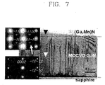
- Figure 7 is a photograph showing a section of the TEM for the (Ga,Mn)N thin film with an Mn concentration of 0.2%.
- Figure 8 is a graph showing lattice constants (a) of several samples measured by a high-order Laue zone (HOLZ) method.
- a standard sample of them is GaN with a thickness of 200 ⁇ m fabricated by hydride vapor phase epitaxy (HVPE) method and has no lattice mismatch by sapphire.
- HVPE hydride vapor phase epitaxy
- comparison between the lattice constants of (Ga,Mn)N and GaN grown by the PEMBE method shows that (Ga,Mn)N is greater than Ga. With this fact, it is confirmed that (Ga,Mn)N is a single (Ga,Mn)N phase formed by substituting Ga with Mn.
- a ferromagnetic semiconductor can be grown by doping a suitable amount of Co, Fe and Ni, the typical ferromagnetic transition element, and Cr, V or the like which has a similar quality to Mn.
- the ferromagnetic semiconductor fabricated in accordance with the present invention can be applicable to various devices.
- Figure 9 is a sectional view showing a structure of a spin LED using a ferromagnetic semiconductor fabricated by the PEMBE method in accordance with the present invention.
- an n-type (or p-type) ferromagnetic semiconductor 81 there are sequentially formed a spacer 82, an insulation layers 83 and 84, a p-type (or n-type) buffer 85, a p-type (or n-type) substrate 86.
- a ferromagnetic semiconductor 93 can be changed to have a ferromagnetic property or to have a non-ferromagnetic property by controlling a carrier concentration with a voltage of a gate 91 so as to be applicable as a Hall effect memory device by using the properties that a Hall resistance is big from an extraordinary Hall effect when the ferromagnetic semiconductor has the ferromagnetic property, while the Hall resistance is small from an ordinary Hall effect when the ferromagnetic semiconductor has the non-ferromagnetic property.
- reference numerals 92 and 94 denote insulation layers
- 95 denotes a buffer layer
- 96 denotes a spin of a material doped in the ferromagnetic semiconductor
- 97 denotes an electron (or Hole).
- the ferromagnetic semiconductor fabricated in accordance with the present invention can be applicable as a spin-polarized field effect transistor (spin FET) by injecting a spin-polarized carrier into a two dimensional electron gas 105 by using a source 101 and a drain 102 of a spin transistor and by using a change in a resistance according to an external magnetic field or controlling a procession of the spin-polarized carrier with a voltage of the gate 103.
- spin FET spin-polarized field effect transistor
- Reference numerals 104 and 106 denote a barrier layer (insulation layer) of a quantum well structure.
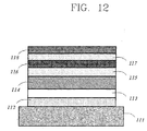
- the ferromagnetic semiconductor fabricated in accordance with the present invention can be applicable to a magnetic tunnelling junction with a structure of ferromagnetic semiconductor/insulation material/ferromagnetic semiconductor.
- Reference numeral 111 denotes a substrate
- 112 denotes a buffer
- 113 denotes a seed layer
- 114 denotes an anti-ferromagnetic layer
- 115 and 117 denote ferromagnetic semiconductor
- 116 denotes a tunnel barrier (insulation layer)
- 118 denotes a capping layer.
- the ferromagnetic semiconductor of the present invention implements the ferromagnetic characteristics even at the room temperature. Therefore, the ferromagnetic semiconductor of the present invention can be adopted to various spin electron devices as a novel ferromagnetic semiconductor implementing a spintronix.
Landscapes
- Engineering & Computer Science (AREA)
- Chemical & Material Sciences (AREA)
- Power Engineering (AREA)
- Nanotechnology (AREA)
- Crystallography & Structural Chemistry (AREA)
- Materials Engineering (AREA)
- Physics & Mathematics (AREA)
- Manufacturing & Machinery (AREA)
- General Physics & Mathematics (AREA)
- Condensed Matter Physics & Semiconductors (AREA)
- Spectroscopy & Molecular Physics (AREA)
- Inorganic Chemistry (AREA)
- Metallurgy (AREA)
- Organic Chemistry (AREA)
- Hall/Mr Elements (AREA)
- Physical Deposition Of Substances That Are Components Of Semiconductor Devices (AREA)
- Hard Magnetic Materials (AREA)
- Crystals, And After-Treatments Of Crystals (AREA)
- Thin Magnetic Films (AREA)
Abstract
Description
- The present invention relates to a room temperature ferromagnetic semiconductor used for a spin electronic device having wide bandgap semiconductor characteristics and magnetic characteristics at a room temperature, its fabrication method, and a ferromagnetic semiconductor based device.
- A research on a GaN-based nitride semiconductor was started to fabricate a blue light emitting device in the early 1990, and currently, researches are being actively conducted on various electronic devices in addition to light emitting and light receiving devices.
- In forming a triple element compound, an energy gap can be controlled from 1.9 eV to 6.2 eV, so that the nitride semiconductor is used for fabrication of a light emitting device of a wave length region of the entire visible light including an ultraviolet ray region. A blue and green light emitting diode (LED) and a ultraviolet ray detector was successfully commercialized years ago, and a blue light emitting diode (LED0 is anticipated to be commercialized soon.
- Meanwhile, research on an electronic device using the nitride semiconductor is actively ongoing. Since a report on a research on a GaN MESFET (metal-semiconductor field effect transistor), a crystal growing technique has been much developed and an electronic device fabrication technique has been also remarkably improved. Diverse researches are being conducted on the electronic device on the basis of excellent physical properties such as a large energy gap, a high thermal and chemical stability, a high electron mobility, a high breakdown voltage and saturation electron speed, the large discontinuation of conduction band, or the like.
- Meanwhile, in view of a novel conceptual spintronics (a compound word of spin and electronics, a fresh paradigm intending to develop an electron and an optical device in consideration of freedom of a spin together with the electronic charge of the electron, a research has been ongoing on the applicability of spintronics in the wake of report on ferromagnetic semiconductor characteristics at a temperature of about 110 K by substituting a portion of Ga in GaAs with Mn, a transition metal, by using a molecular beam epitaxy (MBE) process in the late 1990.
- In this respect, however, (In,Mn)As (Tc = 35K), (Ga,Mn)As (Tc = 110K) and MnGe (Tc = 116 K) are representative ferromagnetic semiconductors which have been studied up to date, but owing to the low Curie temperature, there is a limitation in fabricating a spin device that can be operated at a room temperature. Therefore, finding a ferromagnetic semiconductor with a Curie temperature above a room temperature is the most critical factor in this field.
- According to a theoretical computation result using a Zener model, GaN, ZnO are anticipated to exhibit a Curie temperature above the room temperature, on which, thus, researches are being focussed to testify experimentally.
- Therefore, an aim of the present invention is to provide a semiconductor with magnetic characteristics at a room temperature and its fabrication method.
- Another aim of the present invention is to provide various spin electronic devices using the room temperature ferromagnetic semiconductor.
- To achieve these and other advantages and in accordance with the purpose of the present invention, as embodied and broadly described herein, there is provided a ferromagnetic semiconductor, a 3 group - 5 group compound semiconductor comprising one material 'A' selected from the group of Ga, Al and In and one material 'B' selected from the group consisting of N and P, in which one material 'C' selected from the group consisting of Mn, Mg, Co, Fe, Ni, Cr and V is doped as a material for substituting the material 'A', the compound semiconductor has a single phase on the whole.
- To achieve the above aims, there is further provided a method for fabricating a ferromagnetic semiconductor including the steps of: forming a 3 group - 5 group compound semiconductor thin film comprising one material 'A' selected from the group consisting of Ga, Al and In and one material 'B' selected from the group consisting of N and P; and doping one material 'C' selected from the group consisting of Mn, Mg, Co, Fe, Ni, Cr and V as a material for substituting the material 'A', whiling forming the compound semiconductor thin film by a plasma-enhanced molecular beam epitaxy, wherein the materials 'A' and 'C' are supplied by thermally evaporating from an effusion cell and the material 'B' is supplied from a plasma source.
- The accompanying drawings, which are included to provide a further understanding of the invention and are incorporated in and constitute a part of this specification, illustrate embodiments of the invention and together with the description serve to explain the principles of the invention.
- In the drawings:
- Figure 1 is a schematic view showing a plasma enhanced molecular beam epitaxy (PEMBE) used in the present invention;
- Figure 2 is a graph showing a result of a secondary ion mass spectroscopy (SIMS) measured to observe a Mn distribution in a thin film according to a Mn cell temperature of a (Ga,Mn)N thin film fabricated by the PEMBE method in accordance with the present invention;
- Figure 3 is a graph showing a room temperature hysteresis loop of a (Ga,Mn)N thin film fabricated according to a change in the Mn cell temperature and plasma power in the PEMBE method in accordance with the present invention;
- Figure 4 is a graph showing a hysteresis loop of a (Ga,Mn)N thin flm fabricated under the condition of 670°C /350 W by the PEMBE method in accordance with the present invention;
- Figure 5 is a graph showing a temperature dependency of magnetization of a (Ga,Mn) N thin film with a Mn concentration of 0.16% and 0.50% fabricated by the PEMBE method;
- Figure 6 is a graph showing a change of a magnetic resistance according to magnetic field perpendicular to the thin film for a (Ga,Mn)N thin film fabricated when plasma power is 250W and Mn cell temperatures are 600°C (∘) and 650°C (•) in the PEMBE method;
- Figure 7 is a photograph showing a sectional view of a transmission electron microscope (TEM) and an electron diffraction pattern for a (Ga,Mn)N thin film with a Mn concentration of 0.2% fabricated by the PEMBE method in accordance with the present invention;
- Figure 8 is a graph showing a lattice constant a measured by a high-order Laue zone (HOLZ) method for a ferromagnetic semiconductor fabricated by the PEMBE method in accordance with the present invention;
- Figure 9 is a sectional view showing a structure of a spin LED using a ferromagnetic semiconductor fabricated by the PEMBE method in accordance with the present invention;
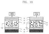
- Figure 10 is a sectional view showing a structure of a Hall effect memory device using the ferromagnetic semiconductor fabricated by the PEMBE method in accordance with the present invention;
- Figure 11 is a sectional view showing a structure of a spin-polarized field effect transistor (spin FET)) using the ferromagnetic semiconductor fabricated by the PEMBE method in accordance with the present invention; and
- Figure 12 is a sectional view showing a magnetic tunnelling junction device with a structure of ferromagnetic semiconductor/insulating material/ferromagnetic semiconductor using the ferromagnetic semiconductor fabricated by the PEMBE method in accordance with the present invention.
-
- As one embodiment of the present invention, a Mn- or Mg-doped GaN thin film was grown by using a plasma-enhanced molecular beam epitaxy device, for which an undoped GaN (GaN templete) grown on a surface of sapphire (0001) by using a metal organic chemical vapor deposition (MOCVD) device was used as a substrate.
- Figure 1 is a schematic view showing the plasma-enhanced molecular beam epitaxy device used in the present invention.
-
Turbomolecular pumps 1 and 2 are connected at the right side and left side of achamber 20, and a substrate 5 is positioned at an upper portion of thechamber 20. The substrate is controlled in its position by asubstrate manipulator 10 formed at an upper portion of the chamber. Aheater 4 is positioned at an upper side of the substrate to control a temperature of the substrate. A liquefied nitrogen (LN2) supply unit 8 is positioned at a lower portion inside the chamber and LN2 covers 9 are attached inside the chamber.Reference numerals 6 and 7 denote, respectively, shutters and 3 denotes a load-lock chamber. - The plasma-enhanced molecular beam epitaxy device is an ultra high vacuum (UHV) system which has a base pressure of 1.2 x 10⁻⁹ torr and exhibits vacuum of about 2 x 10⁻¹⁰ when LN2 is supplied thereto. The rotational substrate manipulator can handle a substrate with a diameter of 3". There are 8 ports at the bottom flange so that
effusion cells RF plasma source 14. - Ga with a purity of 99.99999% (7N) was used to grow the GaN thin film, and Mn (6N) and Mg (6N) were used for doping. N2 (7N) gas was supplied through the RF plasma source. A high purity refractory material, for example, PbN, Mo or the like, was used inside the plasma source to prevent contamination by the high temperature plasma, to which cooling water flew. During the growth of Mn-doped GaN thin film, the temperature of the substrate was 750 ∼ 1000°C, the Mn effusion cell temperature was 600 ∼ 800°C, plasma power was 250 ∼ 350 W, N2 flow rate was 1.5 ~ 2 sccm.
- Hall-measuring of the thusly fabricated (Ga,Mn)N thin film by Van der Pauw method showed that it has characteristics of an n-type semiconductor, its carrier concentration was n = 1016 - 1017/cm3, its electron mobility (µH) was about 103 cm2/Vs, and its non-resistance (ρ) was 0.2Ω cm.
- When Mg was doped in a basic experiment to grow a p-type ferromagnetic semiconductor, the electron concentration was rapidly reduced from ∼2.9 x 1019 cm-3 to ∼4.8 x 1017 cm-3 as FGa/FN flux ratio was increased. It is believed that this is because a compensation effect is increased due to the increase in the Mg concentration according to the increase in the flux ratio. Therefore, it is noted that an Mg-doped GaN thin film of p-type conductance can be grown and p-type ferromagnetic semiconductor can be grown by simultaneously doping Mn and Mg.
- Figure 2 is a graph showing a result of secondary ion mass spectroscopy (SIMS) measured to observe a Mn distribution in a thin film according to a Mn cell temperature of the (Ga,Mn)N thin film.
- As shown in Figure 2, it is noted that Mn in the thin film has an even distribution in the range of 0.7 ∼ 1.0µm. In Addition, it is noted that the Mn concentration in the GaN thin film is increased as the Mn cell temperature goes up. Without a basic sample with an information of Mn concentration, it is not possible to know an accurate Mn concentration for each sample. But from the SIMS result, it can be noted that Mn is effectively doped when GaN is grown. Mn concentration of each sample was indicated as obtained from a magnetic moment measured for each sample. The concentration of the doping material affects a physical property of a magnetization value, and a suitable Mn concentration for growing a single-phase ferromagnetic semiconductor was 0.06 ∼ 3 %.
- Figure 3 shows a hysteresis loop of the (Ga,Mn)N thin film fabricated according to a change in a Mn cell temperature and plasma power as measured at a room temperature with high-sensitivity (10-8 emu) AGM (alternating gradient magnetometer). The Mn cell and plasma power in this context are (a) 630°C/350 W, (b) 650°C/350 W, (c) 650°c/250 W, (d) 650°C/400 W, and (e) 670°C/350 W, respectively.
- It can be observed from the hysteresis loop that the (Ga,Mn)N fabricated in accordance with the present invention have the typical magnetic characteristics at a room temperature.
- In case that the plasma power is 350 W and the Mn cell temperature goes up to 670°C from 630°C, the magnetization value is sharply increased. That is, as the Mn cell temperature is increased, the Mn concentration is increased.
- Meanwhile, in case that the Mn cell temperature is 650°C and the plasma power is changed in the range of 250 ∼ 350, the magnetization value is little changed.
- As the greatest magnetization value, (Ga,Mn)N fabricated with the Mn cell temperature of 670°C and plasma power of 350 W has that Ms = 1.0 emu/cm3 and 0.5 % Mn concentration.
- That is, the magnetization value can be more increased by increasing the concentration of Mn. The temperature of the effusion cell has a great influence on the physical property of the ferromagnetic semiconductor, and an optimum temperature is set depending on a doped material.
- Figure 4 is graph showing an enlarged hysteresis loop of the (Ga,Mn)N thin film fabricated under the condition of 670°C/350 W. As illustrated, a coercive force (Hc) = 69.0e. If there exists a secondary phase such as nano-cluster showing magnetic characteristics in the (Ga,Mn)N thin film, since it exhibits a superparamagnetic behavior, a coercive force can not be expected.
- Therefore, the result of Figure 4 reflects (Ga,Mn)N has a single phase formed by substituting Ga with Mn and this single phase has- the magnetic characteristics at the room temperature.
- Figure 5 is a graph showing a temperature dependency of magnetization of (Ga,Mn)N thin films, respectively, with Mn concentration of 0.16% and 0.50%. The two thin films all show a typical ferromagnetization in 4-300K. According to a computation result by using a mean field theory in order to predict a Curie temperature, each Curie temperature (Tc) shows about 550K and 700 K for (Ga,Mn)N thin films respectively with the Mn concentration of 0.16% and 0.50%. This result tells that a spin device fabricated by using the ferromagnetic (Ga,Mn)N thin film has an enough thermal stability. The picture inserted into a right upper end of Figure 5 shows hysteresis loop that (Ga,Mn)N thin film with an Mn concentration of 0.50% was measured in 4K and 300K.
- Figure 6 shows a magnetoresistance change according to magnetic fields perpendicular to (Ga,Mn)N thin film fabricated when plasma power was 250 W and Mn cell temperatures were 660°C (∘) and 650°C (•). The (Ga,Mn)N thin film fabricated under the two conditions exhibits little resistance change according to the magnetic fields in 300K but exhibits a negative magnetoresistance ofR/R = 10% and

- The picture inserted at the central lower end of Figure 6 shows that the negative magnetoresistance changes according to a temperature in 4 ∼ 300K.
- The negative magnetoresistance is representative characteristics of the ferromagnetic semiconductor, which is much similar to the result of the known (Ga,MN)As (Tc = 110K). With this fact, (Ga,Mn)N fabricated in accordance with the present invention is the semiconductor having the magnetic characteristics at the room temperature. The cause of the negative magnetoresistance is not known yet but widely believed that it is because that a magnetic polaron is formed made up of a carrier and an electron cloud of the Mn spin or because of a Zeeman shift of permi energy.
- Figure 7 is a photograph showing a section of the TEM for the (Ga,Mn)N thin film with an Mn concentration of 0.2%.
- As shown, GaN with a thickness of 2µm grown on a sapphire substrate by the MOCVD method and (Ga,Mn)N grown thereon by the PEMBE method.
- As noted from the electron diffraction pattern inserted to the left portion of Figure 6, there is observed (0-110), (-1100), (1-100), (01-10) additional diffraction spot which are not observed in GaN grown by the MOCVD method.
- This is a phenomenon occurring as Ga is substituted with Mn in the (Ga,Mn)N thin film corresponding to a wurtzite structure among hexagonal structures, showing that Mn shows a single (Ga,Mn)N phase by effectively substituting Ga without forming a secondary phase. Meanwhile, according to the observation result of the TEM, the secondary phase such as the nano cluster was not observed.
- Figure 8 is a graph showing lattice constants (a) of several samples measured by a high-order Laue zone (HOLZ) method. A standard sample of them is GaN with a thickness of 200µm fabricated by hydride vapor phase epitaxy (HVPE) method and has no lattice mismatch by sapphire. As shown, comparison between the lattice constants of (Ga,Mn)N and GaN grown by the PEMBE method shows that (Ga,Mn)N is greater than Ga. With this fact, it is confirmed that (Ga,Mn)N is a single (Ga,Mn)N phase formed by substituting Ga with Mn.
- Meanwhile, as well as Mn, a ferromagnetic semiconductor can be grown by doping a suitable amount of Co, Fe and Ni, the typical ferromagnetic transition element, and Cr, V or the like which has a similar quality to Mn.
- The ferromagnetic semiconductor fabricated in accordance with the present invention can be applicable to various devices.
- Figure 9 is a sectional view showing a structure of a spin LED using a ferromagnetic semiconductor fabricated by the PEMBE method in accordance with the present invention.
- As shown in Figure 9, on an n-type (or p-type)
ferromagnetic semiconductor 81, there are sequentially formed aspacer 82, an insulation layers 83 and 84, a p-type (or n-type)buffer 85, a p-type (or n-type)substrate 86. - in addition, as shown in Figure 10, as for the ferromagnetic semiconductor fabricated in accordance with the present invention, a
ferromagnetic semiconductor 93 can be changed to have a ferromagnetic property or to have a non-ferromagnetic property by controlling a carrier concentration with a voltage of agate 91 so as to be applicable as a Hall effect memory device by using the properties that a Hall resistance is big from an extraordinary Hall effect when the ferromagnetic semiconductor has the ferromagnetic property, while the Hall resistance is small from an ordinary Hall effect when the ferromagnetic semiconductor has the non-ferromagnetic property. In Figure 10,reference numerals - Moreover, as shown in Figure 11, the ferromagnetic semiconductor fabricated in accordance with the present invention can be applicable as a spin-polarized field effect transistor (spin FET) by injecting a spin-polarized carrier into a two
dimensional electron gas 105 by using asource 101 and adrain 102 of a spin transistor and by using a change in a resistance according to an external magnetic field or controlling a procession of the spin-polarized carrier with a voltage of thegate 103. -
Reference numerals - Furthermore, as shown in Figure 12, the ferromagnetic semiconductor fabricated in accordance with the present invention can be applicable to a magnetic tunnelling junction with a structure of ferromagnetic semiconductor/insulation material/ferromagnetic semiconductor.
-
Reference numeral 111 denotes a substrate, 112 denotes a buffer, 113 denotes a seed layer, 114 denotes an anti-ferromagnetic layer, 115 and 117 denote ferromagnetic semiconductor, 116 denotes a tunnel barrier (insulation layer), and 118 denotes a capping layer. - As so far described, unlike the conventional art where the ferromagnetic semiconductor shows characteristics only at a low temperature, the ferromagnetic semiconductor of the present invention implements the ferromagnetic characteristics even at the room temperature. Therefore, the ferromagnetic semiconductor of the present invention can be adopted to various spin electron devices as a novel ferromagnetic semiconductor implementing a spintronix.
- As the present invention may be embodied in several forms without departing from the spirit or essential characteristics thereof, it should also be understood that the above-described embodiments are not limited by any of the details of the foregoing description, unless otherwise specified, but rather should be construed broadly within its spirit and scope as defined in the appended claims, and therefore all changes and modifications that fall within the metes and bounds of the claims, or equivalence of such metes and bounds are therefore intended to be embraced by the appended claims.
Claims (11)
- A 3 group - 5 group compound ferromagnetic semiconductor, comprising one material 'A' selected from the group of Ga, Al and In and one material 'B' selected from the group consisting of N and P,
wherein one material 'C' selected from the group consisting of Mn, Mg, Co, Fe, Ni, Cr and V is doped as a material for substituting the material 'A', the compound semiconductor has a single phase on the whole. - The semiconductor of claim 1, wherein the ferromagnetic semiconductor has its Curie temperature above room temperature.
- A method for fabricating a ferromagnetic semiconductor comprising the steps of:wherein the materials 'A' and 'C' are supplied from an effusion cell and the material 'B' is supplied from a plasma source.forming a 3 group - 5 group compound semiconductor thin film comprising one material 'A' selected from the group consisting of Ga, Al and In and one material 'B' selected from the group consisting of N and P on a substrate; anddoping one material 'C' selected from the group consisting of Mn, Mg, Co, Fe, Ni, Cr and V as a material for substituting the material 'A', while forming the compound semiconductor thin film by a plasma-enhanced molecular beam epitaxy,
- The method of claim 3, wherein the temperature of the effusion cell is 600 ∼ 800°.
- The method of claim 3, wherein the plasma power is 250 ∼ 350 W.
- The method of claim 3, wherein the doping concentration is in the range of 0.06 ~ 3%.
- The method of claim 3, wherein the temperature of the substrate is in the range of 300 ∼ 1000°C.
- A ferromagnetic semiconductor device comprising an insulation layer, a spacer and a ferromagnetic semiconductor sequentially formed on a substrate,
the ferromagnetic semiconductor being a 3 group - 5 group compound semiconductor comprising one material 'A' selected from the group of Ga, Al and In and one material 'B' selected from the group consisting of N and P,
wherein one material 'C' selected from the group consisting of Mn, Mg, Co, Fe, Ni, Cr and V is doped as a material for substituting the material 'A', the compound semiconductor has a single phase on the whole. - A ferromagnetic semiconductor device comprising a gate, an insulation layer formed at a lower side of the gate, and a ferromagnetic semiconductor layer formed at a lower side of the insulation layer,
the ferromagnetic semiconductor being a 3 group - 5 group compound semiconductor comprising one material 'A' selected from the group of Ga, Al and In and one material 'B' selected from the group consisting of N and P,
wherein one material 'C' selected from the group consisting of Mn, Mg, Co, Fe, Ni, Cr and V is doped as a material for substituting the material 'A', the compound semiconductor has a single phase on the whole. - A ferromagnetic semiconductor device comprising a gate, an insulation layer formed at a lower side of the gate, a source and drain region formed at the left and right side of the insulation layer and using a ferromagnetic semiconductor, and a secondary electron gas layer formed at a lower side of the insulation layer,
the ferromagnetic semiconductor being a 3 group - 5 group compound semiconductor comprising one material 'A' selected from the group of Ga, Al and In and one material 'B' selected from the group consisting of N and P,
wherein one material 'C' selected from the group consisting of Mn, Mg, Co, Fe, Ni, Cr and V is doped as a material for substituting the material 'A', the compound semiconductor has a single phase on the whole. - A ferromagnetic semiconductor device comprising a seed layer, an anti-ferromagnetic layer, a ferromagnetic semiconductor layer, an insulation layer and a ferromagnetic semiconductor layer sequentially formed on a substrate,
the ferromagnetic semiconductor being a 3 group - 5 group compound semiconductor comprising one material 'A' selected from the group of Ga, Al and In and one material 'B' selected from the group consisting of N and P,
wherein one material 'C' selected from the group consisting of Mn, Mg, Co, Fe, Ni, Cr and V is doped as a material for substituting the material 'A', the compound semiconductor has a single phase on the whole.
Applications Claiming Priority (2)
| Application Number | Priority Date | Filing Date | Title |
|---|---|---|---|
| KR2002053306 | 2002-09-04 | ||
| KR10-2002-0053306A KR100492482B1 (en) | 2002-09-04 | 2002-09-04 | Room temperature ferromagnetic semiconductor grown by plasma enhanced molecular beam epitaxy and ferromagnetic semiconductor based device |
Publications (2)
| Publication Number | Publication Date |
|---|---|
| EP1396867A1 true EP1396867A1 (en) | 2004-03-10 |
| EP1396867B1 EP1396867B1 (en) | 2008-04-09 |
Family
ID=31713179
Family Applications (1)
| Application Number | Title | Priority Date | Filing Date |
|---|---|---|---|
| EP03250653A Expired - Lifetime EP1396867B1 (en) | 2002-09-04 | 2003-01-31 | Room temperature ferromagnetic semiconductor grown by plasma enhanced molecular beam epitaxy |
Country Status (6)
| Country | Link |
|---|---|
| US (2) | US20040041217A1 (en) |
| EP (1) | EP1396867B1 (en) |
| JP (1) | JP2004104070A (en) |
| KR (1) | KR100492482B1 (en) |
| AT (1) | ATE391997T1 (en) |
| DE (1) | DE60320191T2 (en) |
Cited By (1)
| Publication number | Priority date | Publication date | Assignee | Title |
|---|---|---|---|---|
| WO2014183745A1 (en) * | 2013-05-17 | 2014-11-20 | Helmholtz-Zentrum Dresden - Rossendorf E. V. | Spintronic component |
Families Citing this family (20)
| Publication number | Priority date | Publication date | Assignee | Title |
|---|---|---|---|---|
| JP4477305B2 (en) * | 2002-07-25 | 2010-06-09 | 独立行政法人科学技術振興機構 | Spin transistor and nonvolatile memory using the same |
| KR100681379B1 (en) * | 2003-03-07 | 2007-02-12 | 도꾸리쯔교세이호징 가가꾸 기쥬쯔 신꼬 기꼬 | Field Effect Transistor with Spin-Dependent Transfer Characteristics and Nonvolatile Memory Using the Same |
| EP1610386A4 (en) * | 2003-03-31 | 2009-04-01 | Japan Science & Tech Agency | TUNNEL-EFFECT TRANSISTOR WITH SPIN-DEPENDENT TRANSFER CHARACTERISTICS AND NON-VOLATILE MEMORY USING THE TRANSISTOR |
| KR100666729B1 (en) * | 2005-07-11 | 2007-01-09 | 한국과학기술연구원 | JNS nano belt room temperature magnetic semiconductor manufacturing method |
| FR2898414B1 (en) * | 2006-03-07 | 2008-06-06 | Commissariat Energie Atomique | MAGNETIC FIELD SENSITIVE COMPONENT COMPRISING A DILUTED MAGNETIC SEMICONDUCTOR, INCORPORATING DEVICES AND METHOD FOR CARRYING OUT THE SAME. |
| US20080012004A1 (en) * | 2006-03-17 | 2008-01-17 | Mears Technologies, Inc. | Spintronic devices with constrained spintronic dopant |
| AU2007227418A1 (en) * | 2006-03-17 | 2007-09-27 | Mears Technologies, Inc. | Spintronic devices with constrained spintronic dopant and associated methods |
| US7342244B2 (en) * | 2006-07-19 | 2008-03-11 | Tokyo Electron Limited | Spintronic transistor |
| KR100869290B1 (en) * | 2007-04-25 | 2008-11-18 | 국민대학교산학협력단 | Magnetic Control Method of Magnetic Semiconductor Materials by Proton Injection |
| KR100953532B1 (en) * | 2007-10-09 | 2010-04-21 | 한국과학기술연구원 | Nanomagnetic / Magnetic Semiconductor Hybrid Spin Device and Manufacturing Method Thereof |
| EP2400558A4 (en) * | 2009-02-20 | 2013-08-21 | Nat Univ Corp Kyoto Inst Tech | LIGHT ABSORBING MATERIAL AND PHOTOELECTRIC CONVERSION ELEMENT USING THE SAME |
| KR101039384B1 (en) * | 2009-05-28 | 2011-06-08 | 한국기초과학지원연구원 | Relaxation Oscillator Using Spin Device |
| JP5443502B2 (en) * | 2009-09-18 | 2014-03-19 | 株式会社東芝 | Semiconductor device and manufacturing method thereof |
| EP2549546A4 (en) * | 2010-03-18 | 2017-08-23 | National University Corporation Kyoto Institute of Technology | Light-absorbing material and photoelectric conversion element using same |
| FR2971364B1 (en) * | 2011-02-07 | 2013-02-15 | Centre Nat Rech Scient | OPTIMIZED TRIAZOLE PARTICLE ARRANGEMENT |
| NZ725497A (en) * | 2014-04-02 | 2020-05-29 | Franck Natali | Magnetic materials and devices comprising rare earth nitrides |
| DE102015221521A1 (en) | 2015-11-03 | 2017-05-04 | Forschungszentrum Jülich GmbH | Tunnel diode and transistor |
| US9966901B2 (en) * | 2015-11-19 | 2018-05-08 | Samsung Electronics Co., Ltd. | Spin-torque oscillator based on easy-cone anisotropy |
| CN106637416B (en) * | 2016-12-28 | 2018-11-20 | 厦门大学 | Molecular beam epitaxy and its in-situ characterization device under vector high-intensity magnetic field |
| CN116013961B (en) * | 2023-03-24 | 2023-06-02 | 北京大学 | Preparation method of gallium nitride spin injection junction with self-oxidized surface |
Citations (3)
| Publication number | Priority date | Publication date | Assignee | Title |
|---|---|---|---|---|
| US5294287A (en) * | 1989-05-31 | 1994-03-15 | International Business Machines Corporation | Class of magnetic materials for solid state devices |
| EP1117136A1 (en) * | 1999-07-09 | 2001-07-18 | Japan Science and Technology Corporation | Ferromagnetic double quantum well tunnel magneto-resistance device |
| US20010031547A1 (en) * | 2000-03-07 | 2001-10-18 | Tohoku University | Method of generating spin-polarized conduction electron and semiconductor device |
Family Cites Families (14)
| Publication number | Priority date | Publication date | Assignee | Title |
|---|---|---|---|---|
| JP3556457B2 (en) | 1998-02-20 | 2004-08-18 | 株式会社東芝 | Spin-dependent conductive element and electronic and magnetic components using the same |
| JP4095200B2 (en) | 1998-05-19 | 2008-06-04 | キヤノン株式会社 | Memory device using giant magnetoresistance effect |
| JP4424840B2 (en) | 1999-09-08 | 2010-03-03 | シャープ株式会社 | III-N compound semiconductor device |
| JP2001108951A (en) * | 1999-10-04 | 2001-04-20 | Rikogaku Shinkokai | Optical modulation magnetic semiconductor and its production method |
| US6281538B1 (en) | 2000-03-22 | 2001-08-28 | Motorola, Inc. | Multi-layer tunneling device with a graded stoichiometry insulating layer |
| JP4421065B2 (en) * | 2000-04-07 | 2010-02-24 | 株式会社アルバック | Tunnel magnetoresistive element manufacturing method, tunnel magnetoresistive element |
| JP3736322B2 (en) | 2000-04-26 | 2006-01-18 | 昭和電工株式会社 | Vapor growth equipment |
| US20020075920A1 (en) * | 2000-12-15 | 2002-06-20 | Sylvia Spruytte | Laser diode device with nitrogen incorporating barrier |
| JP2002198615A (en) | 2000-12-25 | 2002-07-12 | Sharp Corp | Semiconductor laser device |
| JP2003137698A (en) | 2001-10-26 | 2003-05-14 | Ulvac Japan Ltd | Iii-v compound semiconductor material |
| US6955858B2 (en) * | 2001-12-07 | 2005-10-18 | North Carolina State University | Transition metal doped ferromagnetic III-V nitride material films and methods of fabricating the same |
| AU2003222000A1 (en) * | 2002-03-14 | 2003-09-29 | Wisys Technology Foundation, Inc. | Mbe-method for the production of a gallium manganese nitride ferromagnetic film |
| KR100483318B1 (en) * | 2002-03-18 | 2005-04-15 | 주식회사 컴텍스 | ferromagnetic - semiconductor single crystal and their manufacturing method |
| US6986693B2 (en) * | 2003-03-26 | 2006-01-17 | Lucent Technologies Inc. | Group III-nitride layers with patterned surfaces |
-
2002
- 2002-09-04 KR KR10-2002-0053306A patent/KR100492482B1/en not_active Expired - Fee Related
-
2003
- 2003-01-14 US US10/342,004 patent/US20040041217A1/en not_active Abandoned
- 2003-01-31 EP EP03250653A patent/EP1396867B1/en not_active Expired - Lifetime
- 2003-01-31 AT AT03250653T patent/ATE391997T1/en not_active IP Right Cessation
- 2003-01-31 DE DE60320191T patent/DE60320191T2/en not_active Expired - Lifetime
- 2003-02-19 JP JP2003041152A patent/JP2004104070A/en active Pending
-
2004
- 2004-08-03 US US10/910,745 patent/US7063986B2/en not_active Expired - Fee Related
Patent Citations (3)
| Publication number | Priority date | Publication date | Assignee | Title |
|---|---|---|---|---|
| US5294287A (en) * | 1989-05-31 | 1994-03-15 | International Business Machines Corporation | Class of magnetic materials for solid state devices |
| EP1117136A1 (en) * | 1999-07-09 | 2001-07-18 | Japan Science and Technology Corporation | Ferromagnetic double quantum well tunnel magneto-resistance device |
| US20010031547A1 (en) * | 2000-03-07 | 2001-10-18 | Tohoku University | Method of generating spin-polarized conduction electron and semiconductor device |
Non-Patent Citations (2)
| Title |
|---|
| OHNO Y ET AL: "ELECTRICAL SPIN INJECTION IN A FERROMAGNETIC SEMICONDUCTOR HETEROSTRUCTURE", NATURE, MACMILLAN JOURNALS LTD. LONDON, GB, vol. 402, no. 6763, 16 December 1999 (1999-12-16), pages 790 - 792, XP000960958, ISSN: 0028-0836 * |
| SONODA S ET AL: "PROPERTIES OF FERROMAGNETIC GA1-XMNXN FILMS GROWN BY AMMONIA-MBE", IEEE TRANSACTIONS ON MAGNETICS, IEEE INC. NEW YORK, US, vol. 38, no. 5, September 2002 (2002-09-01), pages 2859 - 2862, XP001131715, ISSN: 0018-9464 * |
Cited By (2)
| Publication number | Priority date | Publication date | Assignee | Title |
|---|---|---|---|---|
| WO2014183745A1 (en) * | 2013-05-17 | 2014-11-20 | Helmholtz-Zentrum Dresden - Rossendorf E. V. | Spintronic component |
| DE102013209278B4 (en) * | 2013-05-17 | 2016-02-18 | Helmholtz-Zentrum Dresden - Rossendorf E.V. | Magnetizable semiconductors with permanent magnetization and their use |
Also Published As
| Publication number | Publication date |
|---|---|
| US20040041217A1 (en) | 2004-03-04 |
| KR100492482B1 (en) | 2005-06-03 |
| US7063986B2 (en) | 2006-06-20 |
| US20050045976A1 (en) | 2005-03-03 |
| DE60320191D1 (en) | 2008-05-21 |
| JP2004104070A (en) | 2004-04-02 |
| ATE391997T1 (en) | 2008-04-15 |
| KR20040021459A (en) | 2004-03-10 |
| DE60320191T2 (en) | 2009-06-25 |
| EP1396867B1 (en) | 2008-04-09 |
Similar Documents
| Publication | Publication Date | Title |
|---|---|---|
| US7063986B2 (en) | Room temperature ferromagnetic semiconductor grown by plasma enhanced molecular beam epitaxy and ferromagnetic semiconductor based device | |
| Palmstrøm | Epitaxial Heusler alloys: New materials for semiconductor spintronics | |
| Sugahara et al. | Tunneling magnetoresistance in fully epitaxial MnAs/AlAs/MnAs ferromagnetic tunnel junctions grown on vicinal GaAs (111) B substrates | |
| Shayegan et al. | Growth of low‐density two‐dimensional electron system with very high mobility by molecular beam epitaxy | |
| Kane et al. | Magnetic and optical properties of Ga1− x Mn x N grown by metalorganic chemical vapour deposition | |
| US10415153B2 (en) | Doped rare earth nitride materials and devices comprising same | |
| KR20160147791A (en) | Magnetic materials and devices comprising rare earth nitrides | |
| CN105518868B (en) | InGaAlN-based semiconductor element | |
| Newman et al. | Recent progress towards the development of ferromagnetic nitride semiconductors for spintronic applications | |
| US20110186948A1 (en) | Semiconductor-Based Magnetic Material | |
| US6955858B2 (en) | Transition metal doped ferromagnetic III-V nitride material films and methods of fabricating the same | |
| Lu et al. | Molecular-beam-epitaxy growth of ferromagnetic Ni 2 MnGe on GaAs (001) | |
| Xi-Jun et al. | Magnetic and transport properties of ferromagnetic semiconductor GaDyN thin film | |
| US8420407B2 (en) | Growth method of Fe3N material | |
| CA1262293A (en) | Semiconductor super lattice device | |
| Harianto et al. | Epitaxial growth and magnetic properties of Fe3Si/CaF2/Fe3Si tunnel junction structures on CaF2/Si (111) | |
| Ney et al. | Mn-and Cr-doped InN: A promising diluted magnetic semiconductor material | |
| Maji et al. | Spin valve-like magnetic tunnel diode exhibiting giant positive junction magnetoresistance at low temperature in Co2MnSi/SiO2/p-Si heterostructure | |
| Miyao et al. | Molecular beam epitaxial growth of ferromagnetic Heusler alloys for group-IV semiconductor spintronic devices | |
| Chen | Semiconductor Thin Films for Information Technology | |
| JP2008047624A (en) | Antiferromagnetic half-metallic semiconductor | |
| JP5119434B2 (en) | Magnetic semiconductor thin film and method of manufacturing magnetic semiconductor thin film | |
| Dorokhin et al. | Influence of delta doping parameters of the GaAs barrier on circularly polarized luminescence of GaAs/InGaAs heterostructures | |
| Li et al. | Molecular Beam Epitaxy Grown $ Cr_2Te_3 $ Thin Films with Tunable Curie Temperatures | |
| Dorokhin et al. | GaMnSb/InGaAs/GaAs heterostructure leds with a ferromagnetic injector layer |
Legal Events
| Date | Code | Title | Description |
|---|---|---|---|
| PUAI | Public reference made under article 153(3) epc to a published international application that has entered the european phase |
Free format text: ORIGINAL CODE: 0009012 |
|
| 17P | Request for examination filed |
Effective date: 20030210 |
|
| AK | Designated contracting states |
Kind code of ref document: A1 Designated state(s): AT BE BG CH CY CZ DE DK EE ES FI FR GB GR HU IE IT LI LU MC NL PT SE SI SK TR |
|
| AX | Request for extension of the european patent |
Extension state: AL LT LV MK RO |
|
| AKX | Designation fees paid |
Designated state(s): AT BE BG CH CY CZ DE DK EE ES FI FR GB GR HU IE IT LI LU MC NL PT SE SI SK TR |
|
| 17Q | First examination report despatched |
Effective date: 20050802 |
|
| GRAP | Despatch of communication of intention to grant a patent |
Free format text: ORIGINAL CODE: EPIDOSNIGR1 |
|
| RIC1 | Information provided on ipc code assigned before grant |
Ipc: H01F 10/193 20060101ALI20071010BHEP Ipc: H01F 41/30 20060101ALI20071010BHEP Ipc: H01F 1/40 20060101AFI20071010BHEP |
|
| RTI1 | Title (correction) |
Free format text: ROOM TEMPERATURE FERROMAGNETIC SEMICONDUCTOR GROWN BY PLASMA ENHANCED MOLECULAR BEAM EPITAXY |
|
| GRAS | Grant fee paid |
Free format text: ORIGINAL CODE: EPIDOSNIGR3 |
|
| GRAA | (expected) grant |
Free format text: ORIGINAL CODE: 0009210 |
|
| AK | Designated contracting states |
Kind code of ref document: B1 Designated state(s): AT BE BG CH CY CZ DE DK EE ES FI FR GB GR HU IE IT LI LU MC NL PT SE SI SK TR |
|
| REG | Reference to a national code |
Ref country code: GB Ref legal event code: FG4D |
|
| REG | Reference to a national code |
Ref country code: CH Ref legal event code: EP |
|
| REG | Reference to a national code |
Ref country code: IE Ref legal event code: FG4D |
|
| REF | Corresponds to: |
Ref document number: 60320191 Country of ref document: DE Date of ref document: 20080521 Kind code of ref document: P |
|
| PG25 | Lapsed in a contracting state [announced via postgrant information from national office to epo] |
Ref country code: SI Free format text: LAPSE BECAUSE OF FAILURE TO SUBMIT A TRANSLATION OF THE DESCRIPTION OR TO PAY THE FEE WITHIN THE PRESCRIBED TIME-LIMIT Effective date: 20080409 |
|
| NLV1 | Nl: lapsed or annulled due to failure to fulfill the requirements of art. 29p and 29m of the patents act | ||
| PG25 | Lapsed in a contracting state [announced via postgrant information from national office to epo] |
Ref country code: ES Free format text: LAPSE BECAUSE OF FAILURE TO SUBMIT A TRANSLATION OF THE DESCRIPTION OR TO PAY THE FEE WITHIN THE PRESCRIBED TIME-LIMIT Effective date: 20080720 Ref country code: FI Free format text: LAPSE BECAUSE OF FAILURE TO SUBMIT A TRANSLATION OF THE DESCRIPTION OR TO PAY THE FEE WITHIN THE PRESCRIBED TIME-LIMIT Effective date: 20080409 Ref country code: PT Free format text: LAPSE BECAUSE OF FAILURE TO SUBMIT A TRANSLATION OF THE DESCRIPTION OR TO PAY THE FEE WITHIN THE PRESCRIBED TIME-LIMIT Effective date: 20080909 Ref country code: NL Free format text: LAPSE BECAUSE OF FAILURE TO SUBMIT A TRANSLATION OF THE DESCRIPTION OR TO PAY THE FEE WITHIN THE PRESCRIBED TIME-LIMIT Effective date: 20080409 Ref country code: BG Free format text: LAPSE BECAUSE OF FAILURE TO SUBMIT A TRANSLATION OF THE DESCRIPTION OR TO PAY THE FEE WITHIN THE PRESCRIBED TIME-LIMIT Effective date: 20080709 |
|
| PG25 | Lapsed in a contracting state [announced via postgrant information from national office to epo] |
Ref country code: AT Free format text: LAPSE BECAUSE OF FAILURE TO SUBMIT A TRANSLATION OF THE DESCRIPTION OR TO PAY THE FEE WITHIN THE PRESCRIBED TIME-LIMIT Effective date: 20080409 |
|
| ET | Fr: translation filed | ||
| PG25 | Lapsed in a contracting state [announced via postgrant information from national office to epo] |
Ref country code: CZ Free format text: LAPSE BECAUSE OF FAILURE TO SUBMIT A TRANSLATION OF THE DESCRIPTION OR TO PAY THE FEE WITHIN THE PRESCRIBED TIME-LIMIT Effective date: 20080409 Ref country code: SE Free format text: LAPSE BECAUSE OF FAILURE TO SUBMIT A TRANSLATION OF THE DESCRIPTION OR TO PAY THE FEE WITHIN THE PRESCRIBED TIME-LIMIT Effective date: 20080709 Ref country code: DK Free format text: LAPSE BECAUSE OF FAILURE TO SUBMIT A TRANSLATION OF THE DESCRIPTION OR TO PAY THE FEE WITHIN THE PRESCRIBED TIME-LIMIT Effective date: 20080409 |
|
| PLBE | No opposition filed within time limit |
Free format text: ORIGINAL CODE: 0009261 |
|
| STAA | Information on the status of an ep patent application or granted ep patent |
Free format text: STATUS: NO OPPOSITION FILED WITHIN TIME LIMIT |
|
| PG25 | Lapsed in a contracting state [announced via postgrant information from national office to epo] |
Ref country code: BE Free format text: LAPSE BECAUSE OF FAILURE TO SUBMIT A TRANSLATION OF THE DESCRIPTION OR TO PAY THE FEE WITHIN THE PRESCRIBED TIME-LIMIT Effective date: 20080409 Ref country code: SK Free format text: LAPSE BECAUSE OF FAILURE TO SUBMIT A TRANSLATION OF THE DESCRIPTION OR TO PAY THE FEE WITHIN THE PRESCRIBED TIME-LIMIT Effective date: 20080409 |
|
| 26N | No opposition filed |
Effective date: 20090112 |
|
| PG25 | Lapsed in a contracting state [announced via postgrant information from national office to epo] |
Ref country code: EE Free format text: LAPSE BECAUSE OF FAILURE TO SUBMIT A TRANSLATION OF THE DESCRIPTION OR TO PAY THE FEE WITHIN THE PRESCRIBED TIME-LIMIT Effective date: 20080409 |
|
| PG25 | Lapsed in a contracting state [announced via postgrant information from national office to epo] |
Ref country code: MC Free format text: LAPSE BECAUSE OF NON-PAYMENT OF DUE FEES Effective date: 20090131 Ref country code: IT Free format text: LAPSE BECAUSE OF FAILURE TO SUBMIT A TRANSLATION OF THE DESCRIPTION OR TO PAY THE FEE WITHIN THE PRESCRIBED TIME-LIMIT Effective date: 20080409 |
|
| REG | Reference to a national code |
Ref country code: CH Ref legal event code: PL |
|
| PG25 | Lapsed in a contracting state [announced via postgrant information from national office to epo] |
Ref country code: CY Free format text: LAPSE BECAUSE OF FAILURE TO SUBMIT A TRANSLATION OF THE DESCRIPTION OR TO PAY THE FEE WITHIN THE PRESCRIBED TIME-LIMIT Effective date: 20080409 |
|
| PG25 | Lapsed in a contracting state [announced via postgrant information from national office to epo] |
Ref country code: LI Free format text: LAPSE BECAUSE OF NON-PAYMENT OF DUE FEES Effective date: 20090131 Ref country code: CH Free format text: LAPSE BECAUSE OF NON-PAYMENT OF DUE FEES Effective date: 20090131 |
|
| PG25 | Lapsed in a contracting state [announced via postgrant information from national office to epo] |
Ref country code: IE Free format text: LAPSE BECAUSE OF NON-PAYMENT OF DUE FEES Effective date: 20090202 |
|
| PGFP | Annual fee paid to national office [announced via postgrant information from national office to epo] |
Ref country code: FR Payment date: 20100208 Year of fee payment: 8 |
|
| PGFP | Annual fee paid to national office [announced via postgrant information from national office to epo] |
Ref country code: DE Payment date: 20100211 Year of fee payment: 8 Ref country code: GB Payment date: 20100202 Year of fee payment: 8 |
|
| PG25 | Lapsed in a contracting state [announced via postgrant information from national office to epo] |
Ref country code: GR Free format text: LAPSE BECAUSE OF FAILURE TO SUBMIT A TRANSLATION OF THE DESCRIPTION OR TO PAY THE FEE WITHIN THE PRESCRIBED TIME-LIMIT Effective date: 20080710 |
|
| PG25 | Lapsed in a contracting state [announced via postgrant information from national office to epo] |
Ref country code: LU Free format text: LAPSE BECAUSE OF NON-PAYMENT OF DUE FEES Effective date: 20090131 |
|
| PG25 | Lapsed in a contracting state [announced via postgrant information from national office to epo] |
Ref country code: HU Free format text: LAPSE BECAUSE OF FAILURE TO SUBMIT A TRANSLATION OF THE DESCRIPTION OR TO PAY THE FEE WITHIN THE PRESCRIBED TIME-LIMIT Effective date: 20081010 |
|
| PG25 | Lapsed in a contracting state [announced via postgrant information from national office to epo] |
Ref country code: TR Free format text: LAPSE BECAUSE OF FAILURE TO SUBMIT A TRANSLATION OF THE DESCRIPTION OR TO PAY THE FEE WITHIN THE PRESCRIBED TIME-LIMIT Effective date: 20080409 |
|
| GBPC | Gb: european patent ceased through non-payment of renewal fee |
Effective date: 20110131 |
|
| REG | Reference to a national code |
Ref country code: FR Ref legal event code: ST Effective date: 20110930 |
|
| PG25 | Lapsed in a contracting state [announced via postgrant information from national office to epo] |
Ref country code: FR Free format text: LAPSE BECAUSE OF NON-PAYMENT OF DUE FEES Effective date: 20110131 |
|
| PG25 | Lapsed in a contracting state [announced via postgrant information from national office to epo] |
Ref country code: GB Free format text: LAPSE BECAUSE OF NON-PAYMENT OF DUE FEES Effective date: 20110131 |
|
| REG | Reference to a national code |
Ref country code: DE Ref legal event code: R119 Ref document number: 60320191 Country of ref document: DE Effective date: 20110802 |
|
| PG25 | Lapsed in a contracting state [announced via postgrant information from national office to epo] |
Ref country code: DE Free format text: LAPSE BECAUSE OF NON-PAYMENT OF DUE FEES Effective date: 20110802 |