EP1396776A1 - Temperature controller in optical communication device and method for same - Google Patents
Temperature controller in optical communication device and method for same Download PDFInfo
- Publication number
- EP1396776A1 EP1396776A1 EP03020350A EP03020350A EP1396776A1 EP 1396776 A1 EP1396776 A1 EP 1396776A1 EP 03020350 A EP03020350 A EP 03020350A EP 03020350 A EP03020350 A EP 03020350A EP 1396776 A1 EP1396776 A1 EP 1396776A1
- Authority
- EP
- European Patent Office
- Prior art keywords
- temperature
- resistance
- current
- circuited
- short
- Prior art date
- Legal status (The legal status is an assumption and is not a legal conclusion. Google has not performed a legal analysis and makes no representation as to the accuracy of the status listed.)
- Granted
Links
Images


Classifications
-
- G—PHYSICS
- G02—OPTICS
- G02B—OPTICAL ELEMENTS, SYSTEMS OR APPARATUS
- G02B6/00—Light guides; Structural details of arrangements comprising light guides and other optical elements, e.g. couplings
- G02B6/10—Light guides; Structural details of arrangements comprising light guides and other optical elements, e.g. couplings of the optical waveguide type
- G02B6/12—Light guides; Structural details of arrangements comprising light guides and other optical elements, e.g. couplings of the optical waveguide type of the integrated circuit kind
-
- G—PHYSICS
- G02—OPTICS
- G02B—OPTICAL ELEMENTS, SYSTEMS OR APPARATUS
- G02B6/00—Light guides; Structural details of arrangements comprising light guides and other optical elements, e.g. couplings
- G02B6/10—Light guides; Structural details of arrangements comprising light guides and other optical elements, e.g. couplings of the optical waveguide type
- G02B6/12—Light guides; Structural details of arrangements comprising light guides and other optical elements, e.g. couplings of the optical waveguide type of the integrated circuit kind
- G02B6/12007—Light guides; Structural details of arrangements comprising light guides and other optical elements, e.g. couplings of the optical waveguide type of the integrated circuit kind forming wavelength selective elements, e.g. multiplexer, demultiplexer
- G02B6/12009—Light guides; Structural details of arrangements comprising light guides and other optical elements, e.g. couplings of the optical waveguide type of the integrated circuit kind forming wavelength selective elements, e.g. multiplexer, demultiplexer comprising arrayed waveguide grating [AWG] devices, i.e. with a phased array of waveguides
- G02B6/12026—Light guides; Structural details of arrangements comprising light guides and other optical elements, e.g. couplings of the optical waveguide type of the integrated circuit kind forming wavelength selective elements, e.g. multiplexer, demultiplexer comprising arrayed waveguide grating [AWG] devices, i.e. with a phased array of waveguides characterised by means for reducing the temperature dependence
-
- G—PHYSICS
- G02—OPTICS
- G02B—OPTICAL ELEMENTS, SYSTEMS OR APPARATUS
- G02B6/00—Light guides; Structural details of arrangements comprising light guides and other optical elements, e.g. couplings
- G02B6/24—Coupling light guides
- G02B6/42—Coupling light guides with opto-electronic elements
- G02B6/4201—Packages, e.g. shape, construction, internal or external details
-
- G—PHYSICS
- G02—OPTICS
- G02B—OPTICAL ELEMENTS, SYSTEMS OR APPARATUS
- G02B6/00—Light guides; Structural details of arrangements comprising light guides and other optical elements, e.g. couplings
- G02B6/24—Coupling light guides
- G02B6/42—Coupling light guides with opto-electronic elements
- G02B6/4201—Packages, e.g. shape, construction, internal or external details
- G02B6/4266—Thermal aspects, temperature control or temperature monitoring
- G02B6/4268—Cooling
- G02B6/4271—Cooling with thermo electric cooling
-
- G—PHYSICS
- G05—CONTROLLING; REGULATING
- G05D—SYSTEMS FOR CONTROLLING OR REGULATING NON-ELECTRIC VARIABLES
- G05D23/00—Control of temperature
- G05D23/19—Control of temperature characterised by the use of electric means
- G05D23/1906—Control of temperature characterised by the use of electric means using an analogue comparing device
- G05D23/1912—Control of temperature characterised by the use of electric means using an analogue comparing device whose output amplitude can take more than two discrete values
Definitions
- the present invention relates to a temperature controller designed to maintain an optical communication device at a constant temperature regardless of ambient temperature variations.
- optical communication devices such as a laser diode and an Arrayed Wavelength Grating (hereinafter, referred to as AWG) which are used in Wavelength Division Multiplexing (hereinafter, referred to as WDM) are sensitive to ambient temperature variations. It is preferred that optical communication devices as described above employ a temperature controller to maintain a constant temperature, so as to restrict wavelength transition of a transmitted optical signal and stabilize wavelength of a demultiplexed optical signal in WDM optical transmission and WDM-PON (Passive Optical Network) transmission, thereby realizing a stable optical system free from interference from adjacent optical channels.
- WDM optical transmission and WDM-PON Passive Optical Network
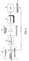
- Fig. 1 is a block diagram showing the construction of a temperature controller in a general optical communication device, in which the temperature controller includes a temperature sensor 10, a temperature comparison section 20, a PID control section 30, a current supply section 40 and a temperature control section 50.
- the temperature sensor 10 detects the current temperature of an optical communication device 60 such as the AWG.
- the temperature sensor utilizes a thermistor, or Pt resistance temperature detector, whose resistance varies according to temperature variations.
- the Pt resistance temperature detector has a Positive Temperature Coefficient (hereinafter, referred to as PTC) in which its resistance increases as temperature rises.
- PTC Positive Temperature Coefficient
- NTC Negative Temperature Coefficient
- the temperature comparison section 20 compares a predetermined temperature with a current temperature and generates an error voltage V err corresponding to the difference between the predetermined and current temperature voltages.
- the temperature controller establishes the predetermined temperature by applying a voltage with a general purpose microcontroller and a Digital-to-Analog Converter (DAC) or directly applying a reference voltage V ref .
- the temperature controller reads a resistance of the temperature sensor 10 attached to the optical communication device 60, such as the AWG, converts the resistance into a current voltage V cur and then compares the current voltage V cur with that of the predetermined temperature so as to obtain the current temperature.
- the compared error voltage is applied to the PID control section 20.
- the PID control section 30 receives the error voltage from the temperature comparison section, adjusts an output voltage so as to conform the current temperature to the predetermined temperature, and applies the output voltage into the current supply section 40.
- the PID control section may selectively use P-, PI-, PD-, PID-control circuits and so on according to temperature variation characteristics.
- the current supply section 40 amplifies the output voltage from the PID control section 30 into a high current using a power operational amplifier (hereinafter, referred to as OPA) or a PWM (Pulse Width Modulation) driver, and supplies the high current to the temperature control section 50.
- OPA power operational amplifier
- PWM Pulse Width Modulation
- the temperature control section 50 controls the temperature of the optical communication device 60, based upon the high current applied from the current supply section 40.
- the polarity of the current applied to the temperature control section 50 is determined by the polarity of the error voltage V err which is the difference between the predetermined and current temperature voltages in the temperature comparison section 20. If the error voltage indicates a positive voltage, a positive current is generated. If the error voltage indicates a negative voltage, a negative current is generated.
- TEC Thermo-Electric Cooler
- the TEC is in the form of a device for heating or cooling an object to be temperature controlled, and used to maintain the temperature of a WDM laser diode.
- the TEC or heater is used for the AWG, in which the heater heats an object to be temperature-controlled regardless of the polarity of the applied current.
- the temperature controller compares the current temperature voltage with the predetermined temperature voltage using an Instrument Amplifier (hereinafter, referred to as IA) circuit so that any error can be precisely amplified via the OP amplifier and the differential amplifier using the OPA.
- IA Instrument Amplifier
- Fig. 2 is a diagram showing a construction of a temperature comparison section of a temperature controller employed in a conventional optical communication device.
- the temperature comparison section utilizes an IA and employs a Pt resistance temperature detector 51 as a temperature sensor will be described below.
- the Pt resistance temperature detector shows a PTC characteristic, that is a resistance variation according to temperature, in which the resistance thereof is 100 ⁇ at 0 °C and increases 0.385 ⁇ for each 1°C rise in temperature.
- a predetermined temperature voltage V1 is set as 1.678V and is input into an anode terminal of the IA 21 while a current temperature voltage is input into a cathode terminal of the IA 21. Then, an output error voltage 22 of the temperature comparison section is applied with a positive polarity into a heater or TEC having a temperature maintenance function with the positive polarity current at a current supply terminal, so as to maintain a desired temperature.
- the temperature comparison section may utilize a thermistor 51 having an NTC characteristic.
- the thermistor shows a resistance of 100k ⁇ at 25°C and about 14.6k ⁇ at 70°C. Where R is 100k ⁇ , the voltage of the set temperature is about 0.382V.
- the set temperature is input into the cathode terminal of the IA while the current temperature voltage is input into an anode terminal of the IA so as to supply current to the TEC or heater through the PID control.
- the current temperature voltage increases approaching the predetermined temperature in the PTC sensor as set forth above while the current temperature voltage decreases to approach the predetermined temperature in the NTC sensor. That is, the current temperature voltage is input into the anode terminal of the IA in the case of the PTC sensor but into the cathode terminal of the IA in the case of the NTC sensor thereby restricting application of the NTC and PTC sensors in a single PCB at the same time.
- One aspect of the present invention is to provide a temperature controller in an optical communication device, including:
- the temperature sensor includes a PTC sensor, and the first and second resistance pads are short-circuited with each other, and the third and fourth resistance pads are short-circuited with each other.
- the temperature sensor includes an NTC sensor, and the first and third resistance pads are short-circuited with each other, and the second and fourth resistance pads are short-circuited with each other.
- the temperature controller further includes at least one resistor of 0 ⁇ for short-circuiting the resistance pads with one another.
- a method of maintaining the temperature of an optical communication device includes the steps of: detecting the current temperature of a device which is to be temperature-controlled; comparing the current temperature to a predetermined temperature to be maintained; generating a signal which represent the difference between the current temperature and the predetermined temperature; and, providing four resistance pads which are selectively short-circuited with one another according to temperature sensor type so as to vary the polarity of the signals input into the differential amplifier.
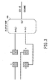
- Fig. 3 is a PCB layout of a temperature comparison section of a temperature controller in an optical communication device of the invention.
- the temperature comparison section of the temperature controller of the invention is designed in such a manner that a differential amplifier 100, e.g. IA and OPA, can execute positive and negative input using resistance pads 1 to 4 at the front end in a single PCB.
- a differential amplifier 100 e.g. IA and OPA
- the resistance pads include the first resistance pad 1 connected to a temperature sensor, the second resistance pad 2 connected to an anode terminal of the differential amplifier 100, the third resistance pad 3 connected to a cathode terminal of the differential amplifier 100, and the fourth resistance pad 4 for receiving a signal corresponding to a set temperature.
- the resistance pads 1 to 4 are arranged so as to be spaced the same vertical and horizontal distance from one another. Based upon a terminal into which the signal is inputted, a procedure for short-circuiting the resistance pads is provided. This procedure will be explained in detail in reference to Figs. 4 and 5 as follows.
- Fig. 4 illustrates a PCB layout where an NTC sensor is used.
- the temperature controller using the NTC sensor has a current temperature voltage larger than a predetermined temperature voltage, and decreases the current temperature voltage through temperature control.
- the current temperature voltage is inputted into the anode terminal of the IA 100 and the predetermined temperature voltage is inputted into the cathode terminal of the IA 100.
- the first and second resistance pads 1 and 2 are short-circuited with each other via a resistor 12 of 0 ⁇ .
- the third and fourth resistance pads 3 and 4 are short-circuited with each other via a resistor 34 of 0 ⁇ .
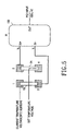
- Fig. 5 illustrates a PCB layout where a PTC temperature sensor is used.
- the temperature controller using the PTC sensor has a current temperature voltage less than a predetermined temperature voltage, and increases the current temperature voltage through temperature control.
- the current temperature voltage is inputted into the cathode terminal of the IA 100 and the predetermined temperature voltage is inputted into the anode terminal of the IA 100.
- the first and third resistance pads 1 and 3 are short-circuited with each other via a resistor 13 of 0 ⁇ .
- the second and fourth resistance pads 2 and 4 are short-circuited with each other via a resistor 24 of 0 ⁇ .
- the present invention can selectively short-circuit the first to fourth resistance pads with one another according to the temperature sensor in use for the temperature controller so as to vary the polarity of signals inputted to the differential amplifier. Therefore, the PTC and NTC sensors can be used simultaneously resulting in a savings of cost and time since the manufacturing of additional PCB's is not necessary.
Landscapes
- Physics & Mathematics (AREA)
- General Physics & Mathematics (AREA)
- Optics & Photonics (AREA)
- Engineering & Computer Science (AREA)
- Microelectronics & Electronic Packaging (AREA)
- Automation & Control Theory (AREA)
- Semiconductor Lasers (AREA)
- Amplifiers (AREA)
- Optical Communication System (AREA)
- Control Of Temperature (AREA)
Abstract
Description
- The present invention relates to a temperature controller designed to maintain an optical communication device at a constant temperature regardless of ambient temperature variations.
- In general, optical communication devices such as a laser diode and an Arrayed Wavelength Grating (hereinafter, referred to as AWG) which are used in Wavelength Division Multiplexing (hereinafter, referred to as WDM) are sensitive to ambient temperature variations. It is preferred that optical communication devices as described above employ a temperature controller to maintain a constant temperature, so as to restrict wavelength transition of a transmitted optical signal and stabilize wavelength of a demultiplexed optical signal in WDM optical transmission and WDM-PON (Passive Optical Network) transmission, thereby realizing a stable optical system free from interference from adjacent optical channels.
- Fig. 1 is a block diagram showing the construction of a temperature controller in a general optical communication device, in which the temperature controller includes a
temperature sensor 10, atemperature comparison section 20, aPID control section 30, acurrent supply section 40 and atemperature control section 50. - The
temperature sensor 10 detects the current temperature of anoptical communication device 60 such as the AWG. The temperature sensor utilizes a thermistor, or Pt resistance temperature detector, whose resistance varies according to temperature variations. The Pt resistance temperature detector has a Positive Temperature Coefficient (hereinafter, referred to as PTC) in which its resistance increases as temperature rises. The thermistor has a PTC or Negative Temperature Coefficient (hereinafter, referred to as NTC) according to the composition of the materials thereof. - The
temperature comparison section 20 compares a predetermined temperature with a current temperature and generates an error voltage Verr corresponding to the difference between the predetermined and current temperature voltages. The temperature controller establishes the predetermined temperature by applying a voltage with a general purpose microcontroller and a Digital-to-Analog Converter (DAC) or directly applying a reference voltage Vref. The temperature controller reads a resistance of thetemperature sensor 10 attached to theoptical communication device 60, such as the AWG, converts the resistance into a current voltage Vcur and then compares the current voltage Vcur with that of the predetermined temperature so as to obtain the current temperature. The compared error voltage is applied to thePID control section 20. - The
PID control section 30 receives the error voltage from the temperature comparison section, adjusts an output voltage so as to conform the current temperature to the predetermined temperature, and applies the output voltage into thecurrent supply section 40. The PID control section may selectively use P-, PI-, PD-, PID-control circuits and so on according to temperature variation characteristics. - The
current supply section 40 amplifies the output voltage from thePID control section 30 into a high current using a power operational amplifier (hereinafter, referred to as OPA) or a PWM (Pulse Width Modulation) driver, and supplies the high current to thetemperature control section 50. - The
temperature control section 50 controls the temperature of theoptical communication device 60, based upon the high current applied from thecurrent supply section 40. The polarity of the current applied to thetemperature control section 50 is determined by the polarity of the error voltage Verr which is the difference between the predetermined and current temperature voltages in thetemperature comparison section 20. If the error voltage indicates a positive voltage, a positive current is generated. If the error voltage indicates a negative voltage, a negative current is generated. Such a temperature controller may include a heater, a Thermo-Electric Cooler (hereinafter, referred to as TEC) and so on. In general, the TEC is in the form of a device for heating or cooling an object to be temperature controlled, and used to maintain the temperature of a WDM laser diode. The TEC or heater is used for the AWG, in which the heater heats an object to be temperature-controlled regardless of the polarity of the applied current. - In the temperature controller having the above construction, it compares the current temperature voltage with the predetermined temperature voltage using an Instrument Amplifier (hereinafter, referred to as IA) circuit so that any error can be precisely amplified via the OP amplifier and the differential amplifier using the OPA.
- Fig. 2 is a diagram showing a construction of a temperature comparison section of a temperature controller employed in a conventional optical communication device. First, the case where the temperature comparison section utilizes an IA and employs a Pt
resistance temperature detector 51 as a temperature sensor will be described below. - The Pt resistance temperature detector shows a PTC characteristic, that is a resistance variation according to temperature, in which the resistance thereof is 100Ω at 0 °C and increases 0.385Ω for each 1°C rise in temperature.
- In conversion of a resistance of the Pt resistance temperature detector into a voltage, where it is supposed that a reference voltage Vref is 3 V, a resistance R is 100Ω , and a predetermined temperature is 70°C, a predetermined temperature voltage V1 is set as 1.678V and is input into an anode terminal of the
IA 21 while a current temperature voltage is input into a cathode terminal of theIA 21. Then, an output error voltage 22 of the temperature comparison section is applied with a positive polarity into a heater or TEC having a temperature maintenance function with the positive polarity current at a current supply terminal, so as to maintain a desired temperature. - Next, the temperature comparison section may utilize a
thermistor 51 having an NTC characteristic. The thermistor shows a resistance of 100kΩ at 25°C and about 14.6kΩ at 70°C. Where R is 100kΩ, the voltage of the set temperature is about 0.382V. The set temperature is input into the cathode terminal of the IA while the current temperature voltage is input into an anode terminal of the IA so as to supply current to the TEC or heater through the PID control. - The current temperature voltage increases approaching the predetermined temperature in the PTC sensor as set forth above while the current temperature voltage decreases to approach the predetermined temperature in the NTC sensor. That is, the current temperature voltage is input into the anode terminal of the IA in the case of the PTC sensor but into the cathode terminal of the IA in the case of the NTC sensor thereby restricting application of the NTC and PTC sensors in a single PCB at the same time.
- It is the object of the present invention to provide a temperature controller in an optical communication device, which can incorporate a PTC sensor and an NTC sensor simultaneously, even while using a single PCB, regardless of the type of temperature sensor.
- This object is solved by the subject matters of the independent claims. Preferred embodiments are defined in the dependent claims.
- One aspect of the present invention is to provide a temperature controller in an optical communication device, including:
- a temperature sensor for detecting the current temperature of a device which is to be temperature-controlled; and, a temperature comparison section for comparing the current temperature detected by the temperature sensor with a predetermined temperature that is a proper operating temperature for the device, wherein the temperature comparison section further includes: a differential amplifier for outputting the difference between signals which are input respectively into anode and cathode terminals; a first resistance pad connected to the temperature sensor; a second resistance pad connected to the anode terminal of the differential amplifier and spaced apart from the first resistance pad; a third resistance pad connected to the cathode terminal of the differential amplifier and spaced apart from the first and second resistance pads; and, a fourth resistance pad for receiving a signal corresponding to the set temperature and spaced apart from the first, second, and third resistance pads, wherein the first to fourth resistance pads are selectively short-circuited with one another according to temperature sensor type so as to vary the polarity of the signals input into the differential amplifier.
-
- In the embodiment, the temperature sensor includes a PTC sensor, and the first and second resistance pads are short-circuited with each other, and the third and fourth resistance pads are short-circuited with each other. The temperature sensor includes an NTC sensor, and the first and third resistance pads are short-circuited with each other, and the second and fourth resistance pads are short-circuited with each other. Further, the temperature controller further includes at least one resistor of 0Ω for short-circuiting the resistance pads with one another.
- In another embodiment of the present invention, a method of maintaining the temperature of an optical communication device is provided is provided. The method includes the steps of: detecting the current temperature of a device which is to be temperature-controlled; comparing the current temperature to a predetermined temperature to be maintained; generating a signal which represent the difference between the current temperature and the predetermined temperature; and, providing four resistance pads which are selectively short-circuited with one another according to temperature sensor type so as to vary the polarity of the signals input into the differential amplifier.
- Fig. 1 is a block diagram illustrating the construction of a temperature controller in a general optical communication device;
- Fig. 2 illustrates a temperature comparison section of a temperature controller in a general optical communication device;
- Fig. 3 is a PCB layout of a temperature comparison section of a temperature controller in an optical communication device of the present invention;
- Fig. 4 is a PCB layout of a temperature comparison section of the present invention using an NTC temperature sensor; and,
- Fig. 5 a PCB layout of a temperature comparison section of the present invention using a PTC temperature sensor.
-
- In accordance with the present invention, a preferred embodiment of the present invention will be described in detail with reference to Figs. 3 to 5. In these drawings, it is to be understood that like reference numerals or symbols refer to like elements even though they are shown in different drawings. For the purposes of clarity and simplicity, well-known functions or constructions will not be described in detail as they would unnecessarily obscure the understanding of the invention.
- Fig. 3 is a PCB layout of a temperature comparison section of a temperature controller in an optical communication device of the invention.
- As shown in Fig. 3, the temperature comparison section of the temperature controller of the invention is designed in such a manner that a
differential amplifier 100, e.g. IA and OPA, can execute positive and negative input usingresistance pads 1 to 4 at the front end in a single PCB. - The resistance pads include the
first resistance pad 1 connected to a temperature sensor, thesecond resistance pad 2 connected to an anode terminal of thedifferential amplifier 100, thethird resistance pad 3 connected to a cathode terminal of thedifferential amplifier 100, and thefourth resistance pad 4 for receiving a signal corresponding to a set temperature. Theresistance pads 1 to 4 are arranged so as to be spaced the same vertical and horizontal distance from one another. Based upon a terminal into which the signal is inputted, a procedure for short-circuiting the resistance pads is provided. This procedure will be explained in detail in reference to Figs. 4 and 5 as follows. - Fig. 4 illustrates a PCB layout where an NTC sensor is used. The temperature controller using the NTC sensor has a current temperature voltage larger than a predetermined temperature voltage, and decreases the current temperature voltage through temperature control. In the temperature controller using the NTC sensor, the current temperature voltage is inputted into the anode terminal of the
IA 100 and the predetermined temperature voltage is inputted into the cathode terminal of theIA 100. - Referring to Fig. 4, in order to input the current temperature detected via the NTC sensor into the anode terminal of the
IA 100, the first andsecond resistance pads resistor 12 of 0Ω . In order to input the predetermined temperature into the cathode terminal of theIA 100, the third andfourth resistance pads resistor 34 of 0Ω . - Fig. 5 illustrates a PCB layout where a PTC temperature sensor is used. The temperature controller using the PTC sensor has a current temperature voltage less than a predetermined temperature voltage, and increases the current temperature voltage through temperature control. In the temperature controller using the PTC sensor, the current temperature voltage is inputted into the cathode terminal of the
IA 100 and the predetermined temperature voltage is inputted into the anode terminal of theIA 100. - Referring to Fig. 5, in order to input the current temperature detected via the PTC sensor into the cathode terminal of the
IA 100, the first andthird resistance pads resistor 13 of 0Ω . In order to input the predetermined temperature into the anode terminal of the IA, the second andfourth resistance pads resistor 24 of 0Ω. - As set forth above, the present invention can selectively short-circuit the first to fourth resistance pads with one another according to the temperature sensor in use for the temperature controller so as to vary the polarity of signals inputted to the differential amplifier. Therefore, the PTC and NTC sensors can be used simultaneously resulting in a savings of cost and time since the manufacturing of additional PCB's is not necessary.
- While the present invention has been shown and described in connection with the preferred embodiment, it is to be understood to those skilled in the art can make various modifications and variations to the present invention without departing from the scope of the appended claims. For example, the voltage applied to the input terminal of the IA or OPA in addition to the temperature controller can be varied according to short-circuiting methods of the resistance pads. Accordingly the scope of the present invention is not be restricted to the foregoing embodiment of the invention but shall be defined by the following claims and equivalents thereof.
Claims (6)
- A temperature controller used in an optical communication device for conforming a current temperature, comprising:a temperature sensor arranged for detecting the current temperature ; anda temperature comparison section adapted for comparing the current temperature detected by the temperature sensor with a predetermined temperature indicative of a proper operating temperature for the device, the temperature comparison section comprising,a differential amplifier adapted for outputting a difference between signals which are inputted respectively into anode and cathode terminals thereof;a first resistance pad connected to the temperature sensor;a second resistance pad connected to the anode terminal of the differential amplifier and spaced from the first resistance pad;a third resistance pad connected to the cathode terminal of the differential amplifier and spaced from the first and second resistance pads; and,a fourth resistance pad arranged for receiving a signal corresponding to the predetermined temperature and spaced from the first, second, and third resistance pads, wherein the first to fourth resistance pads are selectively short-circuited with one another according to a type of the temperature sensor so as to vary the polarity of the signals inputted into the differential amplifier.
- The temperature controller according to claim 1, wherein the temperature sensor comprises an NTC sensor, the first and second resistance pads being short-circuited with each other, and the third and fourth resistance pads being short-circuited with each other.
- The temperature controller according to claim 1, wherein the temperature sensor comprises a PTC sensor, the first and third resistance pads being short-circuited with each other, and the second and fourth resistance pads being short-circuited with each other.
- The temperature controller according to one of claims 1 to 3, further comprising at least one resistor having resistance of 0Ω which short-circuits the resistance pads with one another.
- A method of maintaining the temperature of an optical communication device, comprising:detecting a current temperature of the device;comparing the current temperature to a predetermined temperature;generating a signal which represent a difference between the current temperature and the predetermined temperature; and,providing a plurality of resistance pads that are selectively short-circuited with one another according to a type of the temperature sensor so as to vary the polarity of the signals inputted into the differential amplifier.
- The method according to claim 5, adapted to operate the temperature controller of one of claims 1 to 4.
Applications Claiming Priority (2)
| Application Number | Priority Date | Filing Date | Title |
|---|---|---|---|
| KR10-2002-0054184A KR100433879B1 (en) | 2002-09-09 | 2002-09-09 | Apparatus for temperature controlling of optical communicating device |
| KR2002054184 | 2002-09-09 |
Publications (2)
| Publication Number | Publication Date |
|---|---|
| EP1396776A1 true EP1396776A1 (en) | 2004-03-10 |
| EP1396776B1 EP1396776B1 (en) | 2006-04-12 |
Family
ID=36314070
Family Applications (1)
| Application Number | Title | Priority Date | Filing Date |
|---|---|---|---|
| EP03020350A Expired - Lifetime EP1396776B1 (en) | 2002-09-09 | 2003-09-09 | Temperature controller in optical communication device and method for same |
Country Status (6)
| Country | Link |
|---|---|
| US (1) | US7031356B2 (en) |
| EP (1) | EP1396776B1 (en) |
| JP (1) | JP3959382B2 (en) |
| KR (1) | KR100433879B1 (en) |
| CN (1) | CN1271808C (en) |
| DE (1) | DE60304523T2 (en) |
Cited By (1)
| Publication number | Priority date | Publication date | Assignee | Title |
|---|---|---|---|---|
| EP3812808A4 (en) * | 2018-06-20 | 2022-03-16 | Accelink Technologies Co., Ltd. | ATHERMAL PLANAR SELECTIVE GRID MODULE AND WIDE TEMPERATURE COMPENSATION METHOD |
Families Citing this family (7)
| Publication number | Priority date | Publication date | Assignee | Title |
|---|---|---|---|---|
| DE102004005219A1 (en) * | 2004-02-03 | 2005-08-18 | Baumgärtner, Udo | Device for automation of building technology |
| US7427158B2 (en) * | 2005-01-13 | 2008-09-23 | Kabushiki Kaisha Toshiba | Advanced thermal sensor |
| KR100856923B1 (en) * | 2006-11-08 | 2008-09-05 | 한국전자통신연구원 | Method and apparatus for controling wavelength tuning of optical source for optical communication |
| US7917040B2 (en) | 2006-11-08 | 2011-03-29 | Electronics & Telecommunications Research Institute | Method and apparatus for controlling wavelength tuning of optical source for optical communication |
| DE102008007469A1 (en) * | 2008-02-04 | 2009-08-06 | Airbus Deutschland Gmbh | Extension part for an inlet flap, inlet flap with such an extension part and engine with an inlet flap |
| CN105843282B (en) * | 2016-03-23 | 2018-03-02 | 武汉光迅科技股份有限公司 | A kind of temperature control equipment and method based on FPGA for image intensifer |
| CN111613965A (en) * | 2020-05-20 | 2020-09-01 | 太原理工大学 | A high-precision and high-stability temperature control system for chaotic semiconductor lasers |
Citations (2)
| Publication number | Priority date | Publication date | Assignee | Title |
|---|---|---|---|---|
| FR2288279A1 (en) * | 1974-10-17 | 1976-05-14 | Anvar | Thermostatic control system - has diode as temp. sensor with negative or positive coefficient platinum resistive element |
| EP0703679A2 (en) * | 1994-09-26 | 1996-03-27 | Nippon Telegraph And Telephone Corporation | A multiwavelength simultaneous monitoring circuit employing arrayed-waveguide grating |
Family Cites Families (6)
| Publication number | Priority date | Publication date | Assignee | Title |
|---|---|---|---|---|
| JPS6277604A (en) * | 1985-09-30 | 1987-04-09 | Shimadzu Corp | proportional control device |
| US4922480A (en) * | 1987-12-02 | 1990-05-01 | American Telephone And Telegraph Company | Technique for improving the percentage of semiconductor lasers usable with a predetermined wavelength specification |
| JP2973525B2 (en) * | 1991-01-08 | 1999-11-08 | 日本電気株式会社 | Field effect transistor logic circuit |
| JPH0529841A (en) * | 1991-07-23 | 1993-02-05 | Mitsubishi Electric Corp | Amplifier circuit with temperature compensation |
| US6798341B1 (en) * | 1998-05-18 | 2004-09-28 | Leviton Manufacturing Co., Inc. | Network based multiple sensor and control device with temperature sensing and control |
| US6226114B1 (en) * | 1998-07-02 | 2001-05-01 | Scientific-Atlanta, Inc. | Temperature compensation for uncooled laser |
-
2002
- 2002-09-09 KR KR10-2002-0054184A patent/KR100433879B1/en not_active Expired - Fee Related
-
2003
- 2003-08-18 US US10/642,703 patent/US7031356B2/en not_active Expired - Fee Related
- 2003-08-28 CN CNB03157730XA patent/CN1271808C/en not_active Expired - Fee Related
- 2003-09-09 JP JP2003316607A patent/JP3959382B2/en not_active Expired - Fee Related
- 2003-09-09 DE DE60304523T patent/DE60304523T2/en not_active Expired - Fee Related
- 2003-09-09 EP EP03020350A patent/EP1396776B1/en not_active Expired - Lifetime
Patent Citations (2)
| Publication number | Priority date | Publication date | Assignee | Title |
|---|---|---|---|---|
| FR2288279A1 (en) * | 1974-10-17 | 1976-05-14 | Anvar | Thermostatic control system - has diode as temp. sensor with negative or positive coefficient platinum resistive element |
| EP0703679A2 (en) * | 1994-09-26 | 1996-03-27 | Nippon Telegraph And Telephone Corporation | A multiwavelength simultaneous monitoring circuit employing arrayed-waveguide grating |
Cited By (1)
| Publication number | Priority date | Publication date | Assignee | Title |
|---|---|---|---|---|
| EP3812808A4 (en) * | 2018-06-20 | 2022-03-16 | Accelink Technologies Co., Ltd. | ATHERMAL PLANAR SELECTIVE GRID MODULE AND WIDE TEMPERATURE COMPENSATION METHOD |
Also Published As
| Publication number | Publication date |
|---|---|
| DE60304523D1 (en) | 2006-05-24 |
| KR100433879B1 (en) | 2004-06-04 |
| US20040047397A1 (en) | 2004-03-11 |
| KR20040022578A (en) | 2004-03-16 |
| JP2004104133A (en) | 2004-04-02 |
| EP1396776B1 (en) | 2006-04-12 |
| DE60304523T2 (en) | 2006-08-24 |
| CN1489326A (en) | 2004-04-14 |
| JP3959382B2 (en) | 2007-08-15 |
| CN1271808C (en) | 2006-08-23 |
| US7031356B2 (en) | 2006-04-18 |
Similar Documents
| Publication | Publication Date | Title |
|---|---|---|
| US6229832B1 (en) | Optical wavelength stability control apparatus, optical transmitter and multiple wavelength transmitter | |
| EP1874097B1 (en) | LED circuit with current control | |
| US8155488B2 (en) | Wavelength locking and power control systems for multi-channel photonic integrated circuits (PICs) | |
| EP1061618B1 (en) | Output power controlled wavelength stabilizing system | |
| US7269192B2 (en) | Optical transmitting module and a method for controlling the same | |
| US6944562B2 (en) | Temperature compensation device and method with low heat-generation | |
| US20030033819A1 (en) | Current-Mode control of Thermo-Electric cooler | |
| EP1899754B1 (en) | Feedback system for a monolithic photonic integrated circuit | |
| EP1396776A1 (en) | Temperature controller in optical communication device and method for same | |
| US20060159141A1 (en) | Optical transmitting module operable in wide temperature range | |
| JP2004297615A (en) | Optical receiving circuit | |
| JPH01117385A (en) | Control method for semiconductor laser bias current | |
| EP2178226B1 (en) | Optical transmitter and optical communication system | |
| US8378866B2 (en) | Controller to control electrical power of load in constant | |
| US6947458B2 (en) | Power control circuit for laser diode having wavelength compensation | |
| KR20030008725A (en) | Opitical transmitter having control circuit for optical power/wavelength stability using integrated chip | |
| US20070127530A1 (en) | Laser control | |
| US20090278514A1 (en) | Feedback power control system for an electrical component | |
| US6826210B2 (en) | Power control circuit for laser diode having wavelength compensation | |
| JP2830794B2 (en) | Optical transmission circuit | |
| JPH11251674A (en) | Optical transmitter and control method for optical output and wavelength in the optical transmitter | |
| US20150055946A1 (en) | Method to control transmitter optical module | |
| JP2825628B2 (en) | Monitoring method and stabilization method of modulation degree in optical modulation and optical transmitter | |
| JP2005266282A (en) | Light modulator | |
| GB2218566A (en) | Light emitting package |
Legal Events
| Date | Code | Title | Description |
|---|---|---|---|
| PUAI | Public reference made under article 153(3) epc to a published international application that has entered the european phase |
Free format text: ORIGINAL CODE: 0009012 |
|
| 17P | Request for examination filed |
Effective date: 20030909 |
|
| AK | Designated contracting states |
Kind code of ref document: A1 Designated state(s): AT BE BG CH CY CZ DE DK EE ES FI FR GB GR HU IE IT LI LU MC NL PT RO SE SI SK TR |
|
| AX | Request for extension of the european patent |
Extension state: AL LT LV MK |
|
| AKX | Designation fees paid |
Designated state(s): DE FR GB |
|
| 17Q | First examination report despatched |
Effective date: 20050214 |
|
| GRAP | Despatch of communication of intention to grant a patent |
Free format text: ORIGINAL CODE: EPIDOSNIGR1 |
|
| GRAS | Grant fee paid |
Free format text: ORIGINAL CODE: EPIDOSNIGR3 |
|
| GRAA | (expected) grant |
Free format text: ORIGINAL CODE: 0009210 |
|
| AK | Designated contracting states |
Kind code of ref document: B1 Designated state(s): DE FR GB |
|
| REG | Reference to a national code |
Ref country code: GB Ref legal event code: FG4D |
|
| REF | Corresponds to: |
Ref document number: 60304523 Country of ref document: DE Date of ref document: 20060524 Kind code of ref document: P |
|
| ET | Fr: translation filed | ||
| PLBE | No opposition filed within time limit |
Free format text: ORIGINAL CODE: 0009261 |
|
| STAA | Information on the status of an ep patent application or granted ep patent |
Free format text: STATUS: NO OPPOSITION FILED WITHIN TIME LIMIT |
|
| 26N | No opposition filed |
Effective date: 20070115 |
|
| PGFP | Annual fee paid to national office [announced via postgrant information from national office to epo] |
Ref country code: FR Payment date: 20080915 Year of fee payment: 6 |
|
| PGFP | Annual fee paid to national office [announced via postgrant information from national office to epo] |
Ref country code: GB Payment date: 20080910 Year of fee payment: 6 |
|
| PGFP | Annual fee paid to national office [announced via postgrant information from national office to epo] |
Ref country code: DE Payment date: 20080926 Year of fee payment: 6 |
|
| GBPC | Gb: european patent ceased through non-payment of renewal fee |
Effective date: 20090909 |
|
| REG | Reference to a national code |
Ref country code: FR Ref legal event code: ST Effective date: 20100531 |
|
| PG25 | Lapsed in a contracting state [announced via postgrant information from national office to epo] |
Ref country code: FR Free format text: LAPSE BECAUSE OF NON-PAYMENT OF DUE FEES Effective date: 20090930 Ref country code: DE Free format text: LAPSE BECAUSE OF NON-PAYMENT OF DUE FEES Effective date: 20100401 |
|
| PG25 | Lapsed in a contracting state [announced via postgrant information from national office to epo] |
Ref country code: GB Free format text: LAPSE BECAUSE OF NON-PAYMENT OF DUE FEES Effective date: 20090909 |