EP1394938A1 - Circuit and method for switching gains of preamplifier - Google Patents
Circuit and method for switching gains of preamplifier Download PDFInfo
- Publication number
- EP1394938A1 EP1394938A1 EP02781883A EP02781883A EP1394938A1 EP 1394938 A1 EP1394938 A1 EP 1394938A1 EP 02781883 A EP02781883 A EP 02781883A EP 02781883 A EP02781883 A EP 02781883A EP 1394938 A1 EP1394938 A1 EP 1394938A1
- Authority
- EP
- European Patent Office
- Prior art keywords
- signal
- circuit
- switch
- reference voltage
- output
- Prior art date
- Legal status (The legal status is an assumption and is not a legal conclusion. Google has not performed a legal analysis and makes no representation as to the accuracy of the status listed.)
- Granted
Links
Images




Classifications
-
- H—ELECTRICITY
- H03—ELECTRONIC CIRCUITRY
- H03G—CONTROL OF AMPLIFICATION
- H03G3/00—Gain control in amplifiers or frequency changers
- H03G3/20—Automatic control
- H03G3/30—Automatic control in amplifiers having semiconductor devices
- H03G3/3084—Automatic control in amplifiers having semiconductor devices in receivers or transmitters for electromagnetic waves other than radiowaves, e.g. lightwaves
-
- H—ELECTRICITY
- H03—ELECTRONIC CIRCUITRY
- H03F—AMPLIFIERS
- H03F3/00—Amplifiers with only discharge tubes or only semiconductor devices as amplifying elements
- H03F3/04—Amplifiers with only discharge tubes or only semiconductor devices as amplifying elements with semiconductor devices only
- H03F3/08—Amplifiers with only discharge tubes or only semiconductor devices as amplifying elements with semiconductor devices only controlled by light
- H03F3/087—Amplifiers with only discharge tubes or only semiconductor devices as amplifying elements with semiconductor devices only controlled by light with IC amplifier blocks
-
- H—ELECTRICITY
- H04—ELECTRIC COMMUNICATION TECHNIQUE
- H04B—TRANSMISSION
- H04B10/00—Transmission systems employing electromagnetic waves other than radio-waves, e.g. infrared, visible or ultraviolet light, or employing corpuscular radiation, e.g. quantum communication
- H04B10/60—Receivers
- H04B10/66—Non-coherent receivers, e.g. using direct detection
- H04B10/69—Electrical arrangements in the receiver
- H04B10/695—Arrangements for optimizing the decision element in the receiver, e.g. by using automatic threshold control
-
- H—ELECTRICITY
- H03—ELECTRONIC CIRCUITRY
- H03F—AMPLIFIERS
- H03F2200/00—Indexing scheme relating to amplifiers
- H03F2200/78—A comparator being used in a controlling circuit of an amplifier
Definitions
- the present invention relates to a gain switching circuit and a method of switching gain of a pre-amplifier that is used for a photodetector in an optical communication system, a light signal measuring unit, and a photodetector for a monitor or the like.
- a pre-amplifier is used for a light receiver in an optical communication system.
- the optical communication system is, for example, asynchronous transfer mode-passive optical network (hereinafter, "ATM-PON"), which is an international standard communication system according to the ITU-T recommendation G.983.
- ATM-PON asynchronous transfer mode-passive optical network
- one station can realize a point-to-multi-point transmission with a plurality of subscriber apparatuses with the time division multiplexing, so that transmission can be realized at low cost.
- a pre-amplifier is disclosed, for example, in Japanese Patent Application Laid-open Publication No. 2000-315923 (i.e., burst light receiving circuit).
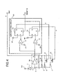
- Fig. 4 is a circuit diagram of the conventional gain switching circuit for a pre-amplifier.
- Fig. 5 is a time chart of operation of the conventional gain switching circuit.
- Fig. 6 is a flowchart of operation of the conventional gain switching circuit.
- a photodetector 1 converts a light signal into an electric signal.
- a pre-amplifier 2 receives the electric signal (i.e., current signal) A.
- This pre-amplifier 2 includes an operation amplifier 2a and a feedback resistor 2b.
- the pre-amplifier 2 is a transimpedance amplifier (hereinafter, "TIA") that amplifies an input current signal and outputs a voltage signal.
- TIA transimpedance amplifier
- the feedback resistor 2b of the TIA 2A is connected in parallel with a serial circuit of a resistor 5 and a diode 8, a serial circuit of a resistor 6 and a switching MOS transistor 9, and a serial circuit of a resistor 7 and a switching MOS transistor 10 respectively.
- a gain switching circuit 31 has identification circuits 11 and 12 and flip-flop circuits 13 and 14, thereby to receive an output (i.e., voltage signal) b from the TIA 2, and control ON and OFF of the MOS transistors 9 and 10 according to the output level.
- the gain switching circuit 31 switches over a feedback resistance of the TIA 2.
- the output (i.e. voltage signal) b from the TIA 2 is input to positive phase input terminals (+) of the identification circuits 11 and 12.
- a reference voltage V1 is input to a negative phase input terminal (-) of the identification circuit 11, and a reference voltage V2 (V1 ⁇ V2) is input to a negative phase input terminal (-) of the identification circuit 12.
- An output terminal of the identification circuit 11 is connected to a clock input terminal C of the flip-flop circuit 13, and a data input terminal D of the flip-flop circuit 13 is connected to a power source VH.
- a signal d output from a data output terminal Q of the flip-flop circuit 13 is applied to a gate electrode of the MOS transistor 9, thereby to turn ON the MOS transistor 9.
- the resistor 6 is connected in parallel to the feedback resistor 2b.
- An output terminal of the identification circuit 12 is connected to a clock input terminal C of the flip-flop circuit 14, and a data input terminal D of the flip-flop circuit 14 is connected to the power source VH.
- a signal e output from a data output terminal Q of the flip-flop circuit 14 is applied to a gate electrode of the MOS transistor 10, thereby to turn ON the MOS transistor 10.
- the resistor 7 is connected in parallel to the feedback resistor 2b.
- An external reset signal (RESET) c is input to a reset terminal R of the flip-flop circuits 13 and 14 respectively.
- the reset signal (RESET) c is input prior to the input of a light burst signal. Therefore, the flip-flop circuits 13 and 14 are initialized at the head of each burst signal. Accordingly, the MOS transistors 9 and 10 are in the OFF (open) operation state at the head of each burst signal.
- (a) is a waveform diagram of current output from the photodetector 1, that is, a waveform of current input to the TIA 2.
- Light burst signals are input to the photodetector 1 in the order of bursts #1, #2, and #3.
- the bursts #1, #2, and #3 are data signals having a bit pattern of "1010" respectively. The amplitude increases in this order.
- (b) is a waveform diagram of a reiationship between a waveform of an output voltage (Vout) b from the TIA 2 and the reference voltages V1 and V2.
- the output voltage (Vout) b from the TIA 2 to the burst #1 is at the reference voltage V1 or below.
- the output voltage (Vout) b from the TIA 2 to the burst #2 exceeds the reference voltage V1, but does not exceed the reference voltage V2.
- the output voltage (Vout) b from the TIA 2 to the burst #3 exceeds the reference voltage V2.
- (c) is a waveform diagram of the reset signal (RESET) c.
- the reset signal (RESET) c is input at the head of the bursts #1, #2, and #3 respectively. Accordingly, the flip-flop circuits 13 and 14 are at the initialized state at the head of each burst signal.
- the MOS transistors 9 and 10 are in the OFF (open) operation state at the head of each burst signal.
- the TIA 2 is in the conversion gain determined by the feedback resistor 2b at the head of each burst signal.
- (d) and (e) are waveform diagrams of the operation of the identification circuits 11 and 12 and the flip-flop circuits 13 and 14.
- the identification circuit 11 does not operate, but the TIA 2 amplifies the burst #1 in the original conversion gain.
- the identification circuit 11 sets the output level from the level “0" to the level "1", and holds this level until when the reset signal (RESET) c is input.
- a signal d of the level "1" is output from the data output terminal Q of the flip-flop circuit 13, and the MOS transistor 9 is turned ON, thereby to connect the resistor 6 in parallel with the feedback resistor 2b.
- the conversion gain of the TIA 2 is switched over from the original conversion gain into a small conversion gain that is determined according to a feedback resistance due to the parallel connection between the feedback resistor 2b and the resistor 6.
- the identification circuit 11 sets the output level from the level "0" to the level "1".
- a signal d of the level "1" is output from the data output terminal Q of the flip-flop circuit 13, and the MOS transistor 9 is turned ON, thereby to connect the resistor 7 in parallel with the feedback resistor 2b.
- the identification circuit 12 sets the output level from the level "0" to the level "1".
- a signal e of the level "1" is output from the data output terminal Q of the flip-flop circuit 14, and the MOS transistor 10 is turned ON, thereby to connect the resistor 7 in parallel with the feedback resistor 2b.
- the conversion gain of the TIA 2 is switched over from the original conversion gain into a smaller conversion gain that is determined according to a feedback resistance due to the parallel connection between the feedback resistor 2b and the resistors 6 and 7.
- the gain switching circuit 31 receives the reset signal (RESET) at the head of the burst signal.
- REET reset signal
- the flip-flop circuits 13 and 14 are reset, and the MOS transistors 9 and 10 are in the OFF state, thereby to return the gain of the TIA 2 to the original conversion gain.
- the output level identification circuits 11 and 12 of the TIA 2 detect whether these signals exceed the respective threshold values V1 and V2 (step S82).
- the gain switching circuit 31 When the output from the TIA 2 is at or below the reference voltage V1 (No at step S83), the gain switching circuit 31 does not turn ON the MOS transistor 9. When the output from the TIA 2 exceeds the reference voltage V1 (Yes at step S83), the gain switching circuit 31 does not turn ON the MOS transistor 9, and maintains the ON state of this transistor (step S84).
- the gain switching circuit 31 When the output from the TIA 2 is lower than the reference voltage V2 (No at step S85), the gain switching circuit 31 does not turn ON the MOS transistor 10. When the output from the TIA 2 is at or above the reference voltage V2 (Yes at step S85), the gain switching circuit 31 does not turn ON the MOS transistor 10, and maintains the ON state of this transistor (step S86).
- the conventional gain switching circuit for a pre-amplifier sets the conversion gain of the TIA 2 to the original gain.
- the conventional gain switching circuit turns ON only the MOS transistor 9, and connects the resistor 6 in parallel with the feedback resistor 2b.
- the conventional gain switching circuit turns ON both the MOS transistors 9 and 10, and connects the resistors 6 and 7 in parallel with the feedback resistor 2b. The conventional gain switching circuit switches over the conversion gain of the TIA 2 in this way.
- the conventional gain switching circuit when the amplitude of the output voltage from the TIA exceeds the reference voltage, the conventional gain switching circuit turns ON the MOS transistor without exception. Therefore, when various kinds of waveform distortions such as ringing, amplitude fluctuation, and signal sag occur, the conventional gain switching circuit does not always switch the gain at the head of the burst signal. There is a possibility that the conventional gain switching circuit switches over the gain at an optional bit position within the burst signal, which makes it difficult to follow the threshold value. Further, depending on the waveform distortion or the like, the conventional gain switching circuit may set the conversion gain to a level different from a target gain.
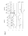
- Fig. 7 is a time chart illustrating an example of a malfunctioning of the conventional gain switching circuit shown in Fig. 4.
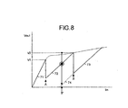
- Fig. 8 is a graph of input-output characteristic of the TIA 2 as the pre-amplifier shown in Fig. 4.
- a' is a waveform of a current output from the photo detector 1, that is, a waveform of a current input to the TIA 2.
- This waveform is of a state that light burst signals of a first burst and a second burst are input in this order to the photo detector 1.
- the first burst and the second burst are data signals having a bit pattern of "1010" respectively.
- the amplitude increases in this order.
- a waveform distortion such as a large ringing is observed at a rising portion of each bit "1".
- b' is an illustration of a relationship between a waveform of the output voltage (Vout) from the TIA 2 and the reference voltages V1 and V2.
- a waveform indicated by a dotted line 61 is a target signal waveform, which is substantially at the same level as the reference voltage V1.
- a waveform indicated by a solid line 62 becomes a cause of generating a malfunctioning. This waveform may or may not exceed the reference voltage V1 at random due to the ringing or the amplitude fluctuation.
- a waveform indicated by a dotted line 63 is a target signal waveform, which exceeds the reference voltage V1 and does not exceed the reference voltage V2.
- a waveform indicated by a solid line 64 becomes a cause of generating a malfunctioning.
- the first bit has a large signal sag Td that exceeds the reference voltage V2.
- Each bit thereafter has a portion large dropped to below the reference voltage V1.
- c' is an illustration of a waveform of a reset signal (RESET).
- the reset signal (RESET) is input at the head of the first burst and the second burst respectively.
- the flip-flop circuits 13 and 14 are initialized at the head of each burst signal.
- the MOS transistors 9 and 10 are in the OFF (closed) operating state at the head of each burst signal.
- the TIA 2 is in the original conversion gain of the TIA 2 that is determined by the feedback resistor 2b.
- d' and e' are waveform diagrams for explaining the operations of the identification circuits 11 and 12, and the flip-flop circuits 13 and 14.
- the identification circuit 11 can correctly recognize this signal waveform at the first bit position. Accordingly, the MOS transistor 9 can be turned ON at the timing of the first bit.
- the MOS transistor 9 can be turned ON at an optional bit position within the burst signal. For example, as indicated by a solid line 66, the MOS transistor 9 is turned ON at a fifth bit position, which causes the conversion gain to be switched over in the middle of the burst signal.
- the MOS transistor maintains the OFF state from the first bit timing, and only the MOS transistor 9 are ON as in d'.
- the identification circuit 12 can correctly recognize this signal waveform at the first bit position as indicated by a solid line 68. Accordingly, the MOS transistor 10 can be turned ON at the timing of the first bit.
- the conversion gain obtained by connecting only the resistor 6 to the feedback resistor 2b in parallel is the target gain.
- the resistor 7 is further set to the conversion gain different from the target gain when the resistor 7 is connected in parallel, which makes the output amplitude smaller than the target amplitude.
- Fig. 8 is an explanatory diagram of the above operation using input-output characteristic of the TIA 2.
- the characteristics 71, 72, and 73 correspond to the operation shown in Fig. 5.
- the characteristic 71 is input-output characteristic when the TIA 2 operates in the original conversion gain as shown by the burst #1.
- the MOS transistor 9 is ON at the gain switching point A as the timing when the amplitude exceeds the reference voltage V1. Therefore, the gain is switched over to change the characteristic to the input-output characteristic 72.
- the MOS transistors 9 and 10 are ON at the gain switching point B as the timing when the amplitude exceeds the reference voltage V2. Therefore, the gain is switched over to change the characteristic to the input-output characteristic 73.
- the first burst is at a level equivalent to the reference voltage V1, that is, a level near the gain switching point A. Therefore, the amplitude exceeds the reference voltage V1 at an optional bit position not only at the first bit position due to the ringing and the amplitude fluctuation of the waveform. Consequently, the MOS transistor 9 is turned ON at an optional bit position within the burst signal.
- the MOS transistors 9 and 10 are turned ON at the first bit position. Therefore, the gain switching point B shifts to a gain switching point B' at the small amplitude side, and the characteristic 73 changes to a characteristic 74 that starts at the gain switching point B' at the small amplitude side. Consequently; the output amplitude becomes much smaller than the target amplitude.
- a gain switching circuit for a pre-amplifier, wherein the pre-amplifier amplifies an output current of a photodetector that converts a burst optical signal into an electrical signal, and outputs an electric voltage signal, and the gain switching circuit is connected with a first serial circuit comprising a first resistor and a first switch and a second serial circuit comprising a second resistor and a second switch, in parallel with a feedback resistor, the gain switching circuit comprising: an arrangement to receive the electric voltage signal output from the pre-amplifier, close the first switch at a specific bit position, close the second switch at the other specific bit position, upon occurrence of a situation that the second switch is to be closed, provided that the first switch is closed.
- the gain switching circuit is connected with a first serial circuit comprising a first resistor and a first switch, and a second serial circuit comprising a second resistor and a second switch, in parallel with a feedback resistor.
- the pre-amplifier amplifies an output current of a photodetector that converts a burst optical signal into an electrical signal, and outputs an electric voltage signal.
- the gain switching circuit comprises: an arrangement to receive the electric voltage signal output from the pre-amplifier, close the first switch at a specific bit position, close the second switch at the other specific bit position, upon occurrence of a situation that the second switch is to be closed, provided that the first switch is closed.
- the gain switching circuit according to the above aspect, wherein the feedback resistor and a serial circuit are connected in parallel with the pre-amplifier, wherein the serial circuit includes a third resistor and a diode.
- the feedback resistor and a serial circuit are connected in parallel with the pre-amplifier, wherein the serial circuit includes a third resistor and a diode.
- the gain switching circuit of the above aspect further comprising: a signal generating unit that generates a first gate signal at the specific bit position, and generates a second gate signal at the other specific bit position, upon occurrence of a situation that the output level of the electric voltage signal exceeds a first reference voltage; a first control unit that closes the first switch, upon occurrence of a situation that an output level of the electric voltage signal exceeds a second reference voltage, and upon occurrence of a situation that a timing at which the output level exceeds the second reference voltage is within a time window of the first gate signal, wherein the second reference voltage is higher than the first reference voltage; and a second control unit that closes the second switch, upon occurrence of a situation that the output level exceeds a third reference voltage, and upon occurrence of a situation that a timing at which the output level exceeds the third reference voltage is within a time window of the second gate signal, wherein the third reference voltage is larger than the second reference voltage.
- a gate signal generating unit generates a first gate signal at the specific bit position, and generates a second gate signal at the other specific bit position, upon occurrence of a situation that the output level of the electric voltage signal exceeds a first reference voltage.
- a first control unit closes the first switch, upon occurrence of a situation that an output level of the electric voltage signal exceeds a second reference voltage, and upon occurrence of a situation that a timing at which the output level exceeds the second reference voltage is within a time window of the first gate signal.
- the second reference voltage is higher than the first reference voltage.
- a second control unit closes the second switch, upon occurrence of a situation that the output level exceeds a third reference voltage, and upon occurrence of a situation that a timing at which the output level exceeds the third reference voltage is within a time window of the second gate signal, wherein the third reference voltage is larger than the second reference voltage.
- the gain switching circuit of the above aspect further comprising: a first level detection circuit that outputs a pulse signal within a time window in which an output level of the electric voltage signal exceeds a first reference voltage; a second level detection circuit that outputs a pulse signal within a time window in which the output level exceeds a second reference voltage, wherein the second reference voltage is higher than the first reference voltage; a third level detection circuit that outputs a pulse signal within a time window in which the output level exceeds a third reference voltage, wherein the third reference voltage is higher than the second reference voltage; a gate signal generation circuit that generates a first gate signal and a second gate signal, wherein a pulse width of the first gate signal is between a falling of a reset signal from an external input and a falling of the pulse signal output from the first level detection circuit corresponding to the specific bit position, and a purse width of the second gate signal is between a falling of the first gate signal and a falling of the pulse signal output from the first level detection
- the output from the pre-amplifier is input to first to third level detection circuits respectively.
- the first level detection circuit outputs a pulse signal within a time window in which an output level of the electric voltage signal exceeds a first reference voltage.
- a gate signal generation circuit generates a first gate signal and a second gate signal, wherein a pulse width of the first gate signal is between a falling of a reset signal from an external input and a falling of the pulse signal output from the first level detection circuit corresponding to the specific bit position, and a purse width of the second gate signal is between a falling of the first gate signal and a falling of the pulse signal output from the first level detection circuit corresponding to the other specific bit position.
- the second level detection circuit outputs a pulse Signal within a time window in which the output level exceeds a second reference voltage, wherein the second reference voltage is higher than the first reference voltage.
- a first judgment circuit outputs a first judgment signal upon inputting of the signal pulse output from the second level detection circuit within the pulse width of the first gate signal. As a result, a first holding circuit holds the first judgment signal until the next input of the reset signal, and closes the first switch.
- the conversion gain of the pre-amplifier is switched over at a specific bit position prescribed by the first gate signal.
- the third level detection circuit outputs a pulse signal within a time window in which the output level exceeds a third reference voltage, wherein the third reference voltage is higher than the second reference voltage.
- a second judgment circuit outputs a second judgment signal upon inputting of the signal pulse output from the third level detection circuit within the pulse width of the second gate signal.
- a second holding circuit holds the second judgment signal until the next input of the reset signal.
- a third judgment circuit closes the second switch, based on the output of the second holding circuit, upon occurrence of a situation that the second holding circuit holds and outputs the second judgment signal while the first holding circuit holds and outputs the first judgment signal.
- the gain switching circuit of the above aspect wherein the first reference voltage is set in such a manner that there is a relatively large voltage difference between the first reference voltage and the second reference voltage, taking a level of waveform distortion that appears in the output signal of the pre-amplifier into consideration.
- the first reference voltage is set in such a manner that there is a relatively large voltage difference between the first reference voltage and the second reference voltage, taking a level of waveform distortion that appears in the output signal of the pre-amplifier into consideration.
- the gain switching circuit of the above aspect wherein the pre-amplifier is further connected with N, where N 3, serial circuits each comprising a third resistor and a third switch in parallel with the feedback resistor, and the gain switching circuit receives the electric voltage signal, and then, upon occurrence of a situation that the third switch of an i th , where 3 i N, serial circuit is to be closed, closes the third switch of the i th serial circuit at a corresponding specific bit position, provided that the third switches of all the serial circuits before the i th serial circuit are closed.
- the pre-amplifier is further connected with N, where N 3, serial circuits each comprising a third resistor and a third switch in parallel with the feedback resistor.
- the gain switching circuit receives the electric voltage signal, and then, upon occurrence of a situation that the third switch of an i th , where 3 i N, serial circuit is to be closed, closes the third switch of the i th serial circuit at a corresponding specific bit position, provided that the third switches of all the serial circuits before the i th serial circuit are closed.
- a method of switching gain of a pre-amplifier wherein the gain is switched by connecting a first serial circuit comprising a first resistor and a first switch and a second serial circuit comprising a second resistor and a second switch, in parallel with a feedback resistor of the pre-amplifier that amplifies an output current of a photodetector that converts a burst optical signal into an electrical signal, and outputs an electric voltage signal, and opening/closing the first switch and the second switch, the method comprising: receiving the electric voltage signal; closing the first switch at a specific bit position based on the electric voltage signal; and closing the second switch, upon occurrence of a situation that the second switch is to be closed, provided that the first switch is closed.
- a first serial circuit comprising a first resistor and a first switch
- a second serial circuit comprising a second resistor and a second switch are connected in parallel with a feedback resistor.
- the pre-amplifier amplifies an output current of a photodetector that converts a burst optical signal into an electrical signal, and outputs an electric voltage signal.
- the gain switching circuit comprises: an arrangement to receive the electric voltage signal output from the pre-amplifier, close the first switch at a specific bit position, close the second switch at the other specific bit position, upon occurrence of a situation that the second switch is to be closed, provided that the first switch is closed.
- the method of switching gain of a pre-amplifier of the above aspect further comprising: closing a third switch of an i th , where 3 i N, serial circuit at a corresponding specific bit position, upon occurrence of a situation that the third switch of the i th serial circuit is to be closed after the gain switching circuit receives the electric voltage signal, provided that third switches of all the serial circuits before the i th serial circuit are closed.
- the method further comprises: closing a third switch of an i th , where 3 i N, serial circuit at a corresponding specific bit position, upon occurrence of a situation that the third switch of the i th serial circuit is to be closed after the gain switching circuit receives the electric voltage signal, provided that third switches of all the serial circuits before the i th serial circuit are closed.
- Fig. 1 is a circuit diagram of a gain switching circuit according to an embodiment of the present invention
- Fig. 2 is a time chart of operation of the gain switching circuit shown in Fig. 1
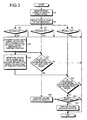
- Fig. 3 is a flowchart illustrating control flow of the gain switching circuit shown in Fig. 1
- Fig. 4 is a circuit diagram of a conventional gain switching circuit
- Fig. 5 is a time chart of operation of the conventional gain switching circuit
- Fig. 6 is a flowchart illustrating control flow of the conventional gain switching circuit
- Fig. 7 is a time chart illustrating an example of a malfunctioning of the conventional gain switching circuit
- Fig. 8 is a graph of input-output characteristic of a pre-amplifier shown in Fig. 4.
- Fig. 1 is a circuit diagram of a gain switching circuit according to an embodiment of the present invention.
- the pre-amplifier 2 that receives an output (i.e., current signal) A from the photodetector 1 that converts a light signal into an electric signal consists of the operation amplifier 2a and the feedback resistor 2b.
- the pre-amplifier 2 is a transimpedance amplifier (TIA) that amplifies an input current signal and outputs a voltage signal.
- TIA transimpedance amplifier
- the feedback resistor 2b of the TIA 2A is connected in parallel with the serial circuit of the resistor 5 and the diode 8, the serial circuit of the resistor 6 and the switching MOS transistor 9 (hereinafter, "SW 9"), and the serial circuit of the resistor 7 and the switching MOS transistor 10 (hereinafter, "SW 10") respectively.
- SW 9 serial circuit of the resistor 6 and the switching MOS transistor 9
- SW 10 serial circuit of the resistor 7 and the switching MOS transistor 10
- the serial circuit of the resistor 5 and the diode 8 may not be provided.
- the conversion gain of the TIA 2 becomes a gain determined by a value of the feedback resistor 2b or a gain determined by a parallel resistance of the feedback resistor 2b and the resistor 5.
- the serial circuit of the resistor 5 and the diode 8 is disregarded, and it is assumed that the gain determined by the value of the feedback resistor 2b is the original conversion gain of the TIA 2.
- the gain switching circuit 3 comprises level detection circuits 15, 16, and 17, a gate generation circuit 18, judgment circuits 19, 20, and 21, and level holding circuits 22 and 23.
- the gain switching circuit 3 switches over the gain at a specific bit position of a burst signal. Thereafter, when a cause of a switching to a different gain occurs, the gain switching circuit 3 does not carry out a single switching operation, but switches the gain at other specific bit position subject to a condition that the gain is switched over at a bit position one before without exception. With this arrangement, the gain is switched over to a suitable conversion gain that fits the level of each burst signal.
- the gain switching circuit 3 switches the gain at a first bit position. Thereafter, when a cause of a gain switching occurs at a third bit position, the gain switching circuit 3 does not carry out a single switching operation, but switches the gain at the third bit position subject to a condition that the gain is switched over at the first bit position without exception.
- An output (i.e., voltage signal) B of the TIA 2 is input to one input terminal of the level detection circuits 15, 16, and 17 respectively.
- a reference voltage V0 as a first reference voltage is input to the other input terminal of the level detection circuit 15.
- a reference voltage V1 as a second reference voltage is input to the other input terminal of the level detection circuit 16.
- a reference voltage V2 as a third reference voltage is input to the other input terminal of the level detection circuit 17.
- An output D from the level detection circuit 15 is input to the gate generation circuit 18.
- Outputs E (i.e., first gate signal) and H (i.e., second gate signal) from the gate generation circuit 18 are input to one input terminal of the judgment circuits 19 and 20 respectively.
- An output F from the level detection circuit 16 is input to the other input terminal of the judgment circuit 19.
- An output I from the level detection circuit 17 is input to the other input terminal of the judgment circuit 20.
- An output from the judgment circuit 19 is input to the level holding circuit 22.
- An output G from the level holding circuit 22 becomes a control signal of the SW 9, and is also input to one input terminal of the judgment circuit 21.
- An output from the judgment circuit 20 is input to the level holding circuit 23.
- An output from the level holding circuit 23 is input to the other input terminal of the judgment circuit 21.
- An output J from the judgment circuit 21 becomes a control signal of the SW 10.
- An external reset signal (RESET) C is input to the gate generation circuit 18 and the level holding circuits 22 and 23 respectively.
- the reset signal (RESET) C is input prior to the input of the optical burst signal, the gate generation circuit 18 and the level holding circuits 22 and 23 are initialized at the head of each burst signal. Therefore, the SW 9 and the SW 10 are in the OFF (open) operation state at the head of each burst signal respectively.
- Fig. 2 is a time chart of an example of the operation of the gain switching circuit shown in Fig. 1.
- Fig. 3 is a flowchart illustrating control flow of the gain switching circuit shown in Fig. 1.
- Fig. 2 is an illustration of the operation of a burst signal in a format similar to that shown in Fig. 5.
- (A) is a waveform diagram of current output from the photodetector 1, that is, a waveform of current input to the TIA 2.
- Light burst signals are input to the photodetector 1 in the order of bursts #1, #2, and #3.
- the bursts #1, #2, and #3 are data signals having a bit pattern of "1010" respectively. The amplitude increases in this order.
- (B) is a waveform diagram of a relationship between a waveform of an output voltage (Vout) B from the TIA 2 and the reference voltages V0, V1, and V2.
- the output voltage (Vout) B from the TIA 2 to the burst #1 is at the reference voltage V0 or below.
- the output voltage (Vout) B from the TIA 2 to the burst #2 exceeds the reference voltage V1, but does not exceed the reference voltage V2.
- the output voltage (Vout) B from the TIA 2 to the burst #3 exceeds the reference voltage V2.
- (C) is a waveform diagram of the reset signal (RESET) C.
- the reset signal (RESET) C is input at the head of the bursts #1, #2, and #3 respectively. Accordingly, the gate generation circuit 18 and the level holding circuits 22 and 23 are at the initialized state at the head of each burst signal.
- the SW 9 and SW 10 are in the OFF (open) operation state at the head of each burst signal.
- the TIA 2 is in the conversion gain determined by the feedback resistor 2b at the head of each burst signal.
- (D) is a waveform diagram of the operation of the level detection circuit 15.
- the output D from the level detection circuit 15 is at the level "0".
- the output D from the level detection circuit 15 fo rms a waveform that alternately repeats the level "1" and the level "0" corresponding to each bit of the burst signal.
- (E) is a waveform diagram of the operation that the gate generation circuit 18 generates the first gate signal E.
- the gate generation circuit 18 is initialized in response to a rise of the reset signal (RESET) C that leads the burst #1, and sets the output to the level "1" in response to a falling of the reset signal (RESET) C.
- the gate generation circuit 18 maintains the output at the level "1" until when the reset signal (RESET) C that leads the burst #1 is input.
- the reset signal (RESET) C is input, the gate generation circuit 18 is initialized, and the circuit 18 sets the output to the level "0".
- the gate generation circuit 18 sets the output E to the level “1” in response to the falling of the reset signal (RESET) C that leads the burst #2. This time, the output from the level detection circuit 15 forms a waveform that alternately repeats the level "1" and the level "0". Therefore, the output from the level detection circuit 15 first becomes at the level "1", and the gate generation circuit 18 maintains the output E at the level "1” until when the output falls to the level "0".
- the gate generation circuit 18 carries out a similar operation in the burst #3.
- the output from the level detection circuit 15 first becomes at the level "1" at the first bit position.
- the gate generation circuit 18 generates the first gate signal E having a pulse width from the falling of the reset signal (RESET) C to the end of the first bit. This first gate signal E is applied to the judgment circuit 19.
- FIG. 2 is a waveform diagram of the operation that the gate generation circuit 18 generates the second gate signal H after generating the first gate signal E.
- the gate generation circuit 18 maintains the output level H at the level "1" during a period from the falling of the first gate signal E until the output from the level detection circuit 15 becomes at the level "1" at the second time and falls to the level "0".
- the output from the level detection circuit 15 becomes at the level "1" at the second time at the third bit position.
- the gate generation circuit 18 generates the second gate signal H having a pulse width from the falling of the first gate signal E to the end of the third bit. This second gate signal H is applied to the judgment circuit 20.
- (F) is a waveform diagram of the operation of the level detection circuit 16.
- the output from the level detection circuit 16 is at the level "0".
- the detection pulse signal F having a pulse width of a time window that exceeds the reference voltage V1 at the timing of the first bit is output to the judgment circuit 19.
- the detection pulse signal F having a pulse width of a time window that exceeds the reference voltage V1 at the timing of the first bit and the third bit respectively is output to the judgment circuit 19.
- (G) is a waveform diagram of the operation of the judgment circuit 19 and the level holding circuit 22.
- the TIA 2 amplifies the original conversion gain in the burst #1.
- the first gate signal E and the detection pulse signal F are input to the judgment circuit 19.
- the judgment circuit 19 outputs the SW control signal to the level holding circuit 22 only when the detection pulse signal F is input to the time window of the first gate signal E.
- the level holding circuit 22 applies the input SW control signal to the gate electrode of the SW 9 as the SW operation signal G, and also outputs the SW control signal to the judgment circuit 21.
- the level holding circuit 22 holds the SW control signal until when the reset signal (RESET) C is input, thereby to keep the SW 9 in the ON state.
- the TIA 2 carries out the switching of the original conversion gain to a small conversion gain that is determined by a parallel resistance of the feedback resistor 2b and the resistor 6, at the first bit position of the burst #2.
- the judgment circuit 19 and the level holding circuit 22 operate, thereby to keep the SW 9 in the ON state.
- the operations shown in Figs. 2I and 2J are carried out in parallel.
- (I) is a waveform diagram of the operation of the level detection circuit 17. As the amplitudes of the burst #1 and the burst #2 are at or below the reference voltage V2, the output from the level detection circuit 17 is at the level "0".
- the detection pulse signal I having a pulse width of a time window that exceeds the reference voltage V2 at the timings of the first bit and the third bit are output to the judgment circuit 20.
- (J) is a waveform diagram of the operations of the judgment circuit 20, the level holding circuit 23, and the judgment circuit 21.
- the judgment circuit 20 outputs the SW control signal to the level holding circuit 23 only when the detection pulse signal I is input to the time window of the second gate signal H. In other words, the detection pulse signal I generated at the first bit position is not within the time window of the second gate signal H, and is therefore invalid.
- the detection pulse signal I generated at the third bit position is within the time window of the second gate signal H, and is therefore valid.
- the level holding circuit 23 outputs the input SW control signal to the judgment circuit 21, and holds this signal until when the reset signal (RESET) C is input.
- the judgment circuit 21 Upon receiving the SW control signal output from the level holding circuit 23, the judgment circuit 21 applies the SW control signal output from the level holding circuit 23 to the gate electrode of the SW 10 as the SW operation signal J, when the SW operation signal G is held at the level "1".
- the TIA 2 carries out the switching of the original conversion gain to a small conversion gain that is determined by a parallel resistance of the feedback resistor 2b and the resistor 6, at the first bit position of the burst #3. Thereafter, at the third bit position, the TIA 2 carries out the switching of the conversion gain to a smaller conversion gain that is determined by a parallel connection further including the resistor 7.
- the second burst has a waveform as indicated by a solid line 64
- the amplitude exceeds the reference voltage V1 and the reference voltage V2 at the first bit position. Therefore, the detection pulse signal F and the detection pulse signal I are generated.
- the first gate signal E is generated, and the second gate signal H is not generated. Accordingly, the gain of the TIA 2 is switched by only the SW 9 at the first bit position, which prevents the SW 10 from being erroneously turned ON.
- the interval between the reference voltage V0 and the reference voltage V1 is set relatively large, by taking into account that the burst signal waveform has various kinds of distortions such as ringing and amplitude fluctuation as shown in Fig. 7. Therefore, even when the signal waveform has a fluctuation, the SW 9 does not switch over the gain until the amplitude reaches a certain level. In other words, it becomes possible to prevent a frequent occurrence of unnecessary switching of gain.
- a SW 1 refers to the SW 9
- a SW 2 refers to the SW 10.
- the gain switching circuit 3 receives the reset signal (RESET) at the head of the burst signal.
- REET reset signal
- the gate generation circuit 18 and the level holding circuits 22 and 23 are reset.
- the SW 1 and the SW 2 are in the OFF state, thereby to return the gain of the TIA 2 to the original conversion gain.
- the level detection circuits 15, 16, and 17 detect whether the output levels of the TIA 2 exceed the respective threshold values V0, V1, and V2 (step S2).
- the SW 1 and the SW 2 are not controlled.
- the gate generation circuit 18 When the output level exceeds the reference voltage V0 (Yes at step S3), the gate generation circuit 18 generates the first gate signal E having a pulse width from the falling of the reset signal (RESET) to the end of the first bit position (step S31). Further, the gate generation circuit 18 generates the second gate signal F having a pulse width from the falling of the first gate signal to the end of the third bit position (step S32).
- RESET reset signal
- the judgment circuit decides whether this exceeding timing coincides with the timing of the first gate signal generated at step S31 (step S41).
- the SW 1 it turned ON, and this ON state is maintained (step S42).
- the control operation ends without turning ON the SW 1.
- the judgment circuit decides whether this exceeding timing coincides with the timing of the second gate signal generated at step S32 (step S51). When these timings do not coincide with each other (No at step S51), the control operation ends without turning ON the SW 2.
- the judgment circuit decides whether the SW 1 is in the ON state at step S42 (step S52). When the SW 1 is in the ON state (Yes at step S52), the SW 2 is turned ON at other specific bit position (i.e., third bit position), and this ON state is maintained (step S53). On the other hand, when the SW 1 is not in the ON state (No at step S52), the control operation ends without turning ON the SW 2.
- the SW 1 is operated at a specific bit position (i.e., first bit position) at which the leading SW 1 is to be operated.
- the SW 2 is operated at a specific bit position (i.e., third bit position). Consequently, both the SW 1 and the SW 2 are securely operated, thereby to obtain a suitable conversion gain.
- the SW 1 is not operated at a specific bit position (i.e., first bit position) at which the leading SW 1 is to be operated, the SW 2 is not operated even if a cause of operating the SW 2 occurs. Consequently, it is possible to prevent the occurrence of an erroneous setting of a conversion gain.
- first bit position and the third bit position are taken up as an example of specific bit positions in the present embodiment, it is also possible to determine these bit positions according to characteristics of the bit pattern and the burst signals that are employed. It is explained in the above that the invention is applied to the pre-amplifier for a photodetector in an optical communication system. It is needless to mention that the invention can also be applied in a similar manner to a pre-amplifier for a light signal measuring unit, and a photo detector for a monitor or the like.
- the present invention is not limited to this assumption. Only one or an optional number of three or more serial circuits of a switch and a resistor may be provided. In other words, an optional number of three or more gain switching circuits 3 are provided to close a third switch of an i th , where 3 i N, serial circuit at a corresponding specific bit position, upon occurrence of a situation that the third switch of the i th serial circuit is to be closed after the gain switching circuit receives the electric voltage signal, provided that third switches of all the serial circuits before the i th serial circuit are closed.
- the gain switching circuit is connected with a first serial circuit comprising a first resistor and a first switch, and a second serial circuit comprising a second resistor and a second switch, in parallel with a feedback resistor.
- the pre-amplifier amplifies an output current of a photodetector that converts a burst optical signal into an electrical signal, and outputs an electric voltage signal.
- the gain switching circuit comprises: an arrangement to receive the electric voltage signal output from the pre-amplifier, close the first switch at a specific bit position, close the second switch at the other specific bit position, upon occurrence of a situation that the second switch is to be closed, provided that the first switch is closed.
- the conversion gain can be securely switched at a specific bit position of the burst signal. Further, it is possible to securely prevent the occurrence of a switching of the conversion gain at an optional bit position within the burst signal.
- the second switch can be closed subject to the condition that the leading first switch is operated. Therefore, a proper conversion gain can be set, and an erroneous setting of the conversion gain can be prevented.
- the feedback resistor and a serial circuit are connected in parallel with the pre-amplifier, wherein the serial circuit includes a third resistor and a diode. Therefore, the conversion gain can be automatically switched according to a size of the input amplitude of the pre-amplifier.
- a gate signal generating unit generates a first gate signal at the specific bit position, and generates a second gate signal at the other specific bit position, upon occurrence of a situation that the output level of the electric voltage signal exceeds a first reference voltage.
- a first control unit closes the first switch, upon occurrence of a situation that an output level of the electric voltage signal exceeds a second reference voltage, and upon occurrence of a situation that a timing at which the output level exceeds the second reference voltage is within a time window of the first gate signal.
- the second reference voltage is higher than the first reference voltage.
- a second control unit closes the second switch, upon occurrence of a situation that the output level exceeds a third reference voltage, and upon occurrence of a situation that a timing at which the output level exceeds the third reference voltage is within a time window of the second gate signal, wherein the third reference voltage is larger than the second reference voltage. Therefore, the conversion gain can be securely switched at a specific bit position prescribed by the first gate signal. Further, it is possible to securely prevent the occurrence of a switching of the conversion gain at an optional bit position within the burst signal.
- the second switch can be closed at a specific bit position prescribed by the second gate signal subject to the condition that the leading first switch is operated. Therefore, a proper conversion gain can be set, and an erroneous setting of the conversion gain can be prevented.
- the output from the pre-amplifier is input to first to third level detection circuits respectively.
- the first level detection circuit outputs a pulse signal within a time window in which an output level of the electric voltage signal exceeds a first reference voltage.
- a gate signal generation circuit generates a first gate signal and a second gate signal, wherein a pulse width of the first gate signal is between a falling of a reset signal from an external input and a falling of the pulse signal output from the first level detection circuit corresponding to the specific bit position, and a purse width of the second gate signal is between a falling of the first gate signal and a falling of the pulse signal output from the first level detection circuit corresponding to the other specific bit position.
- the second level detection circuit outputs a pulse signal within a time window in which the output level exceeds a second reference voltage, wherein the second reference voltage is higher than the first reference voltage.
- a first judgment circuit outputs a first judgment signal upon inputting of the signal pulse output from the second level detection circuit within the pulse width of the first gate signal. As a result, a first holding circuit holds the first judgment signal until the next input of the reset signal, and closes the first switch.
- the conversion gain of the pre-amplifier is switched over at a specific bit position prescribed by the first gate signal.
- the third level detection circuit outputs a pulse signal within a time window in which the output level exceeds a third reference voltage, wherein the third reference voltage is higher than the second reference voltage.
- a second judgment circuit outputs a second judgment signal upon inputting of the signal pulse output from the third level detection circuit within the pulse width of the second gate signal.
- a second holding circuit holds the second judgment signal until the next input of the reset signal.
- a third judgment circuit closes the second switch, based on the output of the second holding circuit, upon occurrence of a situation that the second holding circuit holds and outputs the second judgment signal while the first holding circuit holds and outputs the first judgment signal.
- the first reference voltage is set in such a manner that there is a relatively large voltage difference between the first reference voltage and the second reference voltage, taking a level of waveform distortion that appears in the output signal of the pre-amplifier into consideration. Therefore, it is possible to prevent a frequent occurrence of unnecessary switching of a conversion gain.
- the pre-amplifier is further connected with N, where N 3, serial circuits each comprising a third resistor and a third switch in parallel with the feedback resistor.
- the gain switching circuit receives the electric voltage signal, and then, upon occurrence of a situation that the third switch of an i th , where 3 i N, serial circuit is to be closed, closes the third switch of the i th serial circuit at a corresponding specific bit position, provided that the third switches of all the serial circuits before the i th serial circuit are closed. Therefore, the switching of a conversion gain can be controlled more accurately.
- a first serial circuit comprising a first resistor and a first switch
- a second serial circuit comprising a second resistor and a second switch are connected in parallel with a feedback resistor.
- the pre-amplifier amplifies an output current of a photodetector that converts a burst optical signal into an electrical signal, and outputs an electric voltage signal.
- the gain switching circuit comprises: an arrangement to receive the electric voltage signal output from the pre-amplifier, close the first switch at a specific bit position, close the second switch at the other specific bit position, upon occurrence of a situation that the second switch is to be closed, provided that the first switch is closed. Therefore, the conversion gain can be securely switched at a specific bit position of the burst signal.
- the second switch can be closed subject to the condition that the leading first switch is operated. Therefore, a proper conversion gain can be set, and an erroneous setting of the conversion gain can be prevented.
- the method further comprises: closing a third switch of an i th , where 3 i N, serial circuit at a corresponding specific bit position, upon occurrence of a situation that the third switch of the i th serial circuit is to be closed after the gain switching circuit receives the electric voltage signal, provided that third switches of all the serial circuits before the i th serial circuit are closed. Therefore, the switching of a conversion gain can be controlled more accurately.
- the gain switching circuit and the method of switching gain of a pre-amplifier can be suitably applied to a photodetector in an optical communication system, a light signal measuring unit, and a photodetector for a monitor or the like.
Landscapes
- Engineering & Computer Science (AREA)
- Physics & Mathematics (AREA)
- Electromagnetism (AREA)
- Power Engineering (AREA)
- Computer Networks & Wireless Communication (AREA)
- Signal Processing (AREA)
- Control Of Amplification And Gain Control (AREA)
- Amplifiers (AREA)
- Optical Communication System (AREA)
Abstract
Description
According to still another aspect of the present invention, there is provided the method of switching gain of a pre-amplifier of the above aspect, the method further comprising: closing a third switch of an ith, where 3 i N, serial circuit at a corresponding specific bit position, upon occurrence of a situation that the third switch of the ith serial circuit is to be closed after the gain switching circuit receives the electric voltage signal, provided that third switches of all the serial circuits before the ith serial circuit are closed.
According to the above aspect of the invention, the method further comprises: closing a third switch of an ith, where 3 i N, serial circuit at a corresponding specific bit position, upon occurrence of a situation that the third switch of the ith serial circuit is to be closed after the gain switching circuit receives the electric voltage signal, provided that third switches of all the serial circuits before the ith serial circuit are closed.
Claims (9)
- A gain switching circuit for a pre-amplifier, wherein
the pre-amplifier amplifies an output current of a photodetector that converts a burst optical signal into an electrical signal, and outputs an electric voltage signal, and the gain switching circuit is connected with a first serial circuit comprising a first resistor and a first switch and a second serial circuit comprising a second resistor and a second switch, in parallel with a feedback resistor, the gain switching circuit comprising:an arrangement to receive the electric voltage signal output from the pre-amplifier, close the first switch at a specific bit position, close the second switch at the other specific bit position, upon occurrence of a situation that the second switch is to be closed, provided that the first switch is closed. - The gain switching circuit according to claim 1, wherein the feedback resistor and a serial circuit are connected in parallel with the pre-amplifier, wherein the serial circuit includes a third resistor and a diode.
- The gain switching circuit according to claim 1, further comprising:a signal generating unit that generates a first gate signal at the specific bit position, and generates a second gate signal at the other specific bit position, upon occurrence of a situation that the output level of the electric voltage signal exceeds a first reference voltage;a first control unit that closes the first switch, upon occurrence of a situation that an output level of the electric voltage signal exceeds a second reference voltage, and upon occurrence of a situation that a timing at which the output level exceeds the second reference voltage is within a time window of the first gate signal, wherein the second reference voltage is higher than the first reference voltage; anda second control unit that closes the second switch, upon occurrence of a situation that the output level exceeds a third reference voltage, and upon occurrence of a situation that a timing at which the output level exceeds the third reference voltage is within a time window of the second gate signal, wherein the third reference voltage is larger than the second reference voltage.
- The gain switching circuit according to claim 3, wherein the first reference voltage is set in such a manner that there is a relatively large voltage difference between the first reference voltage and the second reference voltage, taking a level of waveform distortion that appears in the output signal of the pre-amplifier into consideration.
- The gain switching circuit according to claim 1, further comprising:a first level detection circuit that outputs a pulse signal within a time window in which an output level of the electric voltage signal exceeds a first reference voltage;a second level detection circuit that outputs a pulse signal within a time window in which the output level exceeds a second reference voltage, wherein the second reference voltage is higher than the first reference voltage;a third level detection circuit that outputs a pulse signal within a time window in which the output level exceeds a third reference voltage, wherein the third reference voltage is higher than the second reference voltage;a gate signal generation circuit that generates a first gate signal and a second gate signal, wherein a pulse width of the first gate signal is between a falling of a reset signal from an external input and a falling of the pulse signal output from the first level detection circuit corresponding to the specific bit position, and a purse width of the second gate signal is between a falling of the first gate signal and a falling of the pulse signal output from the first level detection circuit corresponding to the other specific bit position;a first judgment circuit that outputs a first judgment signal upon inputting of the signal pulse output from the second level detection circuit within the pulse width of the first gate signal;a first holding circuit that holds the first judgment signal until the next input of the reset signal, and closes the first switch;a second judgment circuit that outputs a second judgment signal upon inputting of the signal pulse output from the third level detection circuit within the pulse width of the second gate signal;a second holding circuit that holds the second judgment signal until the next input of the reset signal; anda third judgment circuit that closes the second switch, based on the output of the second holding circuit, upon occurrence of a situation that the second holding circuit holds and outputs the second judgment signal while the first holding circuit holds and outputs the first judgment signal.
- The gain switching circuit according to claim 5, wherein the first reference voltage is set in such a manner that there is a relatively large voltage difference between the first reference voltage and the second reference voltage, taking a level of waveform distortion that appears in the output signal of the pre-amplifier into consideration.
- The gain switching circuit according to claim 1, wherein
the pre-amplifier is further connected with N, where N 3, serial circuits each comprising a third resistor and a third switch in parallel with the feedback resistor, and
the gain switching circuit receives the electric voltage signal, and then, upon occurrence of a situation that the third switch of an ith, where 3 i N, serial circuit is to be closed, closes the third switch of the ith serial circuit at a corresponding specific bit position, provided that the third switches of all the serial circuits before the ith serial circuit are closed. - A method of switching gain of a pre-amplifier, wherein
the gain is switched by connecting a first serial circuit comprising a first resistor and a first switch and a second serial circuit comprising a second resistor and a second switch, in parallel with a feedback resistor of the pre-amplifier that amplifies an output current of a photodetector that converts a burst optical signal into an electrical signal, and outputs an electric voltage signal, and opening/closing the first switch and the second switch, the method comprising:receiving the electric voltage signal;closing the first switch at a specific bit position based on the electric voltage signal; andclosing the second switch, upon occurrence of a situation that the second switch is to be closed, provided that the first switch is closed. - The method according to claim 8, further comprising:closing a third switch of an ith, where 3 i N, serial circuit at a corresponding specific bit position, upon occurrence of a situation that the third switch of the ith serial circuit is to be closed after the gain switching circuit receives the electric voltage signal, provided that third switches of all the serial circuits before the ith serial circuit are closed.
Applications Claiming Priority (3)
| Application Number | Priority Date | Filing Date | Title |
|---|---|---|---|
| JP2002041944A JP4169985B2 (en) | 2002-02-19 | 2002-02-19 | Preamplifier gain switching circuit |
| JP2002041944 | 2002-02-19 | ||
| PCT/JP2002/012684 WO2003071674A1 (en) | 2002-02-19 | 2002-12-03 | Circuit and method for switching gains of preamplifier |
Publications (3)
| Publication Number | Publication Date |
|---|---|
| EP1394938A1 true EP1394938A1 (en) | 2004-03-03 |
| EP1394938A4 EP1394938A4 (en) | 2005-12-07 |
| EP1394938B1 EP1394938B1 (en) | 2007-08-15 |
Family
ID=27750477
Family Applications (1)
| Application Number | Title | Priority Date | Filing Date |
|---|---|---|---|
| EP02781883A Expired - Lifetime EP1394938B1 (en) | 2002-02-19 | 2002-12-03 | System including a gain switching circuit and method of switching gain of pre-amplifier |
Country Status (5)
| Country | Link |
|---|---|
| US (1) | US6989717B2 (en) |
| EP (1) | EP1394938B1 (en) |
| JP (1) | JP4169985B2 (en) |
| DE (1) | DE60221824T2 (en) |
| WO (1) | WO2003071674A1 (en) |
Cited By (4)
| Publication number | Priority date | Publication date | Assignee | Title |
|---|---|---|---|---|
| WO2005124996A3 (en) * | 2004-06-18 | 2006-03-30 | Melexis Nv | Dvd reading apparatus |
| EP1805915A4 (en) * | 2004-10-26 | 2009-01-14 | Optoelectronics Co Ltd | A preamplifier circuit having a variable feedback resistance |
| WO2009138127A1 (en) * | 2008-05-15 | 2009-11-19 | Telefonaktiebolaget Lm Ericsson (Publ) | Agc low threshold signal level detection |
| DE102008053293B3 (en) * | 2008-10-27 | 2010-06-02 | Atmel Automotive Gmbh | Trans-impedance converter for connection of photodiode for optical device, has amplifier unit, feedback device which is connected with amplifier unit output and amplifier unit input |
Families Citing this family (8)
| Publication number | Priority date | Publication date | Assignee | Title |
|---|---|---|---|---|
| US7358818B2 (en) * | 2003-10-20 | 2008-04-15 | Sumitomo Electric Industries, Ltd. | Optical receiver for an optical communication |
| JP4088679B2 (en) * | 2004-08-03 | 2008-05-21 | 日本電信電話株式会社 | Receiving method and receiving circuit |
| JP4546348B2 (en) * | 2005-07-22 | 2010-09-15 | 日本電信電話株式会社 | Transimpedance amplifier |
| KR100826882B1 (en) * | 2005-12-05 | 2008-05-06 | 한국전자통신연구원 | Digital automatic gain controller method and apparatus in bust mode optical receiver |
| JP2010136030A (en) * | 2008-12-03 | 2010-06-17 | Panasonic Corp | Received-light amplifying circuit and optical disc device |
| EP2388933A4 (en) * | 2009-01-19 | 2014-06-25 | Hitachi Ltd | TRANSIMPEDANCE AMPLIFIER AND PON SYSTEM |
| GB2523854B (en) * | 2014-05-23 | 2016-06-08 | Hilight Semiconductor Ltd | Circuitry |
| US10778170B2 (en) | 2018-11-10 | 2020-09-15 | Semtech Corporation | Automatic gain control for passive optical network |
Family Cites Families (11)
| Publication number | Priority date | Publication date | Assignee | Title |
|---|---|---|---|---|
| SE380150B (en) * | 1974-02-18 | 1975-10-27 | Bofors Ab | |
| JPH0629755A (en) * | 1992-07-10 | 1994-02-04 | Mitsubishi Electric Corp | Preamplifier |
| US5952883A (en) * | 1996-10-25 | 1999-09-14 | Nec Corporation | Circuit arrangement for amplifying an electrical signal converted from an optical signal |
| JPH11340745A (en) * | 1998-05-28 | 1999-12-10 | Nec Corp | Trans impedance type amplifier circuit |
| JP2000151290A (en) * | 1998-11-05 | 2000-05-30 | Nec Corp | Initial-stage amplifying circuit |
| JP3259707B2 (en) | 1999-02-26 | 2002-02-25 | 日本電気株式会社 | Burst mode optical receiver with AGC |
| JP2000315923A (en) | 1999-04-30 | 2000-11-14 | Nec Corp | Burst light receiving circuit |
| JP3456574B2 (en) | 1999-11-10 | 2003-10-14 | 日本電気株式会社 | Burst mode optical receiving system and method |
| JP2001196877A (en) | 2000-01-06 | 2001-07-19 | Mitsubishi Electric Corp | Preamplifier circuit |
| JP2001217657A (en) * | 2000-02-01 | 2001-08-10 | Oki Electric Ind Co Ltd | Preamplifier for optical communication |
| US6246284B1 (en) * | 2000-02-15 | 2001-06-12 | Oki Electric Industry Co., Ltd. | Negative feedback amplifier with automatic gain control function |
-
2002
- 2002-02-19 JP JP2002041944A patent/JP4169985B2/en not_active Expired - Fee Related
- 2002-12-03 DE DE60221824T patent/DE60221824T2/en not_active Expired - Lifetime
- 2002-12-03 EP EP02781883A patent/EP1394938B1/en not_active Expired - Lifetime
- 2002-12-03 WO PCT/JP2002/012684 patent/WO2003071674A1/en not_active Ceased
- 2002-12-03 US US10/477,945 patent/US6989717B2/en not_active Expired - Fee Related
Cited By (5)
| Publication number | Priority date | Publication date | Assignee | Title |
|---|---|---|---|---|
| WO2005124996A3 (en) * | 2004-06-18 | 2006-03-30 | Melexis Nv | Dvd reading apparatus |
| EP1805915A4 (en) * | 2004-10-26 | 2009-01-14 | Optoelectronics Co Ltd | A preamplifier circuit having a variable feedback resistance |
| WO2009138127A1 (en) * | 2008-05-15 | 2009-11-19 | Telefonaktiebolaget Lm Ericsson (Publ) | Agc low threshold signal level detection |
| US8849224B2 (en) | 2008-05-15 | 2014-09-30 | Optis Cellular Technology, Llc | AGC low threshold signal level detection |
| DE102008053293B3 (en) * | 2008-10-27 | 2010-06-02 | Atmel Automotive Gmbh | Trans-impedance converter for connection of photodiode for optical device, has amplifier unit, feedback device which is connected with amplifier unit output and amplifier unit input |
Also Published As
| Publication number | Publication date |
|---|---|
| EP1394938A4 (en) | 2005-12-07 |
| JP2003243955A (en) | 2003-08-29 |
| US20040145419A1 (en) | 2004-07-29 |
| EP1394938B1 (en) | 2007-08-15 |
| US6989717B2 (en) | 2006-01-24 |
| WO2003071674A1 (en) | 2003-08-28 |
| DE60221824T2 (en) | 2008-04-30 |
| JP4169985B2 (en) | 2008-10-22 |
| DE60221824D1 (en) | 2007-09-27 |
Similar Documents
| Publication | Publication Date | Title |
|---|---|---|
| US7218865B2 (en) | Burst-mode optical receiver of differential output structure | |
| EP1394938A1 (en) | Circuit and method for switching gains of preamplifier | |
| EP2096754B1 (en) | Optical receiver | |
| US20100272448A1 (en) | Optical burst signal receiving device | |
| JP2009188499A (en) | Optical burst receiver and optical burst reception method | |
| US7266312B2 (en) | Burst mode optical receiver | |
| US5952883A (en) | Circuit arrangement for amplifying an electrical signal converted from an optical signal | |
| CN100414843C (en) | Burst Mode Receiver with Offset Compensation Function and Data Restoration Method | |
| CN1993885B (en) | transconductance amplifier | |
| JP2008236455A (en) | Transimpedance amplifier and control method of transimpedance amplifier | |
| JP3259707B2 (en) | Burst mode optical receiver with AGC | |
| JP2000315923A (en) | Burst light receiving circuit | |
| US7003043B2 (en) | Replica driver mismatch correction using a variable offset comparator | |
| CN100463362C (en) | Receiving method and receiving circuit | |
| US7598479B2 (en) | Circuit for varying gain of preamplifier | |
| JP4546348B2 (en) | Transimpedance amplifier | |
| JP3927352B2 (en) | Burst receiver | |
| JPH08139526A (en) | Optical receiver | |
| JP2005123350A (en) | Average power detection circuit, laser diode drive circuit, and optical transmission module | |
| JP3191746B2 (en) | Optical receiving circuit | |
| JPH07193437A (en) | Gain switching type optical receiver / amplifier circuit | |
| JPS6369336A (en) | optical receiver circuit | |
| CN117318817A (en) | Signal detection quick response circuit with hysteresis control |
Legal Events
| Date | Code | Title | Description |
|---|---|---|---|
| PUAI | Public reference made under article 153(3) epc to a published international application that has entered the european phase |
Free format text: ORIGINAL CODE: 0009012 |
|
| 17P | Request for examination filed |
Effective date: 20031120 |
|
| AK | Designated contracting states |
Kind code of ref document: A1 Designated state(s): AT BE BG CH CY CZ DE DK EE ES FI FR GB GR IE IT LI LU MC NL PT SE SI SK TR |
|
| A4 | Supplementary search report drawn up and despatched |
Effective date: 20051024 |
|
| RAP1 | Party data changed (applicant data changed or rights of an application transferred) |
Owner name: MITSUBISHI DENKI KABUSHIKI KAISHA |
|
| GRAP | Despatch of communication of intention to grant a patent |
Free format text: ORIGINAL CODE: EPIDOSNIGR1 |
|
| RTI1 | Title (correction) |
Free format text: SYSTEM INCLUDING A GAIN SWITCHING CIRCUIT AND METHOD OF SWITCHING GAIN OF PRE-AMPLIFIER |
|
| GRAS | Grant fee paid |
Free format text: ORIGINAL CODE: EPIDOSNIGR3 |
|
| RIN1 | Information on inventor provided before grant (corrected) |
Inventor name: NOGAMI, MASAMICHI Inventor name: MOTOSHIMA KUNIAKI |
|
| GRAA | (expected) grant |
Free format text: ORIGINAL CODE: 0009210 |
|
| AK | Designated contracting states |
Kind code of ref document: B1 Designated state(s): DE FR GB IT |
|
| REG | Reference to a national code |
Ref country code: GB Ref legal event code: FG4D |
|
| REF | Corresponds to: |
Ref document number: 60221824 Country of ref document: DE Date of ref document: 20070927 Kind code of ref document: P |
|
| ET | Fr: translation filed | ||
| PLBE | No opposition filed within time limit |
Free format text: ORIGINAL CODE: 0009261 |
|
| STAA | Information on the status of an ep patent application or granted ep patent |
Free format text: STATUS: NO OPPOSITION FILED WITHIN TIME LIMIT |
|
| 26N | No opposition filed |
Effective date: 20080516 |
|
| REG | Reference to a national code |
Ref country code: GB Ref legal event code: 746 Effective date: 20090305 |
|
| PGFP | Annual fee paid to national office [announced via postgrant information from national office to epo] |
Ref country code: GB Payment date: 20101201 Year of fee payment: 9 |
|
| PGFP | Annual fee paid to national office [announced via postgrant information from national office to epo] |
Ref country code: IT Payment date: 20111216 Year of fee payment: 10 |
|
| GBPC | Gb: european patent ceased through non-payment of renewal fee |
Effective date: 20121203 |
|
| PG25 | Lapsed in a contracting state [announced via postgrant information from national office to epo] |
Ref country code: GB Free format text: LAPSE BECAUSE OF NON-PAYMENT OF DUE FEES Effective date: 20121203 |
|
| PG25 | Lapsed in a contracting state [announced via postgrant information from national office to epo] |
Ref country code: IT Free format text: LAPSE BECAUSE OF NON-PAYMENT OF DUE FEES Effective date: 20121203 |
|
| PGFP | Annual fee paid to national office [announced via postgrant information from national office to epo] |
Ref country code: DE Payment date: 20131127 Year of fee payment: 12 |
|
| PGFP | Annual fee paid to national office [announced via postgrant information from national office to epo] |
Ref country code: FR Payment date: 20131209 Year of fee payment: 12 |
|
| REG | Reference to a national code |
Ref country code: DE Ref legal event code: R119 Ref document number: 60221824 Country of ref document: DE |
|
| REG | Reference to a national code |
Ref country code: FR Ref legal event code: ST Effective date: 20150831 |
|
| PG25 | Lapsed in a contracting state [announced via postgrant information from national office to epo] |
Ref country code: DE Free format text: LAPSE BECAUSE OF NON-PAYMENT OF DUE FEES Effective date: 20150701 |
|
| PG25 | Lapsed in a contracting state [announced via postgrant information from national office to epo] |
Ref country code: FR Free format text: LAPSE BECAUSE OF NON-PAYMENT OF DUE FEES Effective date: 20141231 |