EP1394912A1 - Nitride semiconductor laser - Google Patents
Nitride semiconductor laser Download PDFInfo
- Publication number
- EP1394912A1 EP1394912A1 EP02730913A EP02730913A EP1394912A1 EP 1394912 A1 EP1394912 A1 EP 1394912A1 EP 02730913 A EP02730913 A EP 02730913A EP 02730913 A EP02730913 A EP 02730913A EP 1394912 A1 EP1394912 A1 EP 1394912A1
- Authority
- EP
- European Patent Office
- Prior art keywords
- layer
- type
- semiconductor laser
- nitride semiconductor
- laser according
- Prior art date
- Legal status (The legal status is an assumption and is not a legal conclusion. Google has not performed a legal analysis and makes no representation as to the accuracy of the status listed.)
- Granted
Links
Images



Classifications
-
- H—ELECTRICITY
- H01—ELECTRIC ELEMENTS
- H01S—DEVICES USING THE PROCESS OF LIGHT AMPLIFICATION BY STIMULATED EMISSION OF RADIATION [LASER] TO AMPLIFY OR GENERATE LIGHT; DEVICES USING STIMULATED EMISSION OF ELECTROMAGNETIC RADIATION IN WAVE RANGES OTHER THAN OPTICAL
- H01S5/00—Semiconductor lasers
- H01S5/30—Structure or shape of the active region; Materials used for the active region
- H01S5/34—Structure or shape of the active region; Materials used for the active region comprising quantum well or superlattice structures, e.g. single quantum well [SQW] lasers, multiple quantum well [MQW] lasers or graded index separate confinement heterostructure [GRINSCH] lasers
- H01S5/343—Structure or shape of the active region; Materials used for the active region comprising quantum well or superlattice structures, e.g. single quantum well [SQW] lasers, multiple quantum well [MQW] lasers or graded index separate confinement heterostructure [GRINSCH] lasers in AIIIBV compounds, e.g. AlGaAs-laser, InP-based laser
- H01S5/34333—Structure or shape of the active region; Materials used for the active region comprising quantum well or superlattice structures, e.g. single quantum well [SQW] lasers, multiple quantum well [MQW] lasers or graded index separate confinement heterostructure [GRINSCH] lasers in AIIIBV compounds, e.g. AlGaAs-laser, InP-based laser with a well layer based on Ga(In)N or Ga(In)P, e.g. blue laser
-
- B—PERFORMING OPERATIONS; TRANSPORTING
- B82—NANOTECHNOLOGY
- B82Y—SPECIFIC USES OR APPLICATIONS OF NANOSTRUCTURES; MEASUREMENT OR ANALYSIS OF NANOSTRUCTURES; MANUFACTURE OR TREATMENT OF NANOSTRUCTURES
- B82Y20/00—Nanooptics, e.g. quantum optics or photonic crystals
-
- H—ELECTRICITY
- H01—ELECTRIC ELEMENTS
- H01S—DEVICES USING THE PROCESS OF LIGHT AMPLIFICATION BY STIMULATED EMISSION OF RADIATION [LASER] TO AMPLIFY OR GENERATE LIGHT; DEVICES USING STIMULATED EMISSION OF ELECTROMAGNETIC RADIATION IN WAVE RANGES OTHER THAN OPTICAL
- H01S2301/00—Functional characteristics
- H01S2301/17—Semiconductor lasers comprising special layers
- H01S2301/173—The laser chip comprising special buffer layers, e.g. dislocation prevention or reduction
-
- H—ELECTRICITY
- H01—ELECTRIC ELEMENTS
- H01S—DEVICES USING THE PROCESS OF LIGHT AMPLIFICATION BY STIMULATED EMISSION OF RADIATION [LASER] TO AMPLIFY OR GENERATE LIGHT; DEVICES USING STIMULATED EMISSION OF ELECTROMAGNETIC RADIATION IN WAVE RANGES OTHER THAN OPTICAL
- H01S2304/00—Special growth methods for semiconductor lasers
- H01S2304/12—Pendeo epitaxial lateral overgrowth [ELOG], e.g. for growing GaN based blue laser diodes
-
- H—ELECTRICITY
- H01—ELECTRIC ELEMENTS
- H01S—DEVICES USING THE PROCESS OF LIGHT AMPLIFICATION BY STIMULATED EMISSION OF RADIATION [LASER] TO AMPLIFY OR GENERATE LIGHT; DEVICES USING STIMULATED EMISSION OF ELECTROMAGNETIC RADIATION IN WAVE RANGES OTHER THAN OPTICAL
- H01S5/00—Semiconductor lasers
- H01S5/04—Processes or apparatus for excitation, e.g. pumping, e.g. by electron beams
- H01S5/042—Electrical excitation ; Circuits therefor
- H01S5/0421—Electrical excitation ; Circuits therefor characterised by the semiconducting contacting layers
-
- H—ELECTRICITY
- H01—ELECTRIC ELEMENTS
- H01S—DEVICES USING THE PROCESS OF LIGHT AMPLIFICATION BY STIMULATED EMISSION OF RADIATION [LASER] TO AMPLIFY OR GENERATE LIGHT; DEVICES USING STIMULATED EMISSION OF ELECTROMAGNETIC RADIATION IN WAVE RANGES OTHER THAN OPTICAL
- H01S5/00—Semiconductor lasers
- H01S5/10—Construction or shape of the optical resonator, e.g. extended or external cavity, coupled cavities, bent-guide, varying width, thickness or composition of the active region
- H01S5/1082—Construction or shape of the optical resonator, e.g. extended or external cavity, coupled cavities, bent-guide, varying width, thickness or composition of the active region with a special facet structure, e.g. structured, non planar, oblique
-
- H—ELECTRICITY
- H01—ELECTRIC ELEMENTS
- H01S—DEVICES USING THE PROCESS OF LIGHT AMPLIFICATION BY STIMULATED EMISSION OF RADIATION [LASER] TO AMPLIFY OR GENERATE LIGHT; DEVICES USING STIMULATED EMISSION OF ELECTROMAGNETIC RADIATION IN WAVE RANGES OTHER THAN OPTICAL
- H01S5/00—Semiconductor lasers
- H01S5/30—Structure or shape of the active region; Materials used for the active region
- H01S5/305—Structure or shape of the active region; Materials used for the active region characterised by the doping materials used in the laser structure
- H01S5/3072—Diffusion blocking layer, i.e. a special layer blocking diffusion of dopants
-
- H—ELECTRICITY
- H01—ELECTRIC ELEMENTS
- H01S—DEVICES USING THE PROCESS OF LIGHT AMPLIFICATION BY STIMULATED EMISSION OF RADIATION [LASER] TO AMPLIFY OR GENERATE LIGHT; DEVICES USING STIMULATED EMISSION OF ELECTROMAGNETIC RADIATION IN WAVE RANGES OTHER THAN OPTICAL
- H01S5/00—Semiconductor lasers
- H01S5/30—Structure or shape of the active region; Materials used for the active region
- H01S5/32—Structure or shape of the active region; Materials used for the active region comprising PN junctions, e.g. hetero- or double- heterostructures
- H01S5/3201—Structure or shape of the active region; Materials used for the active region comprising PN junctions, e.g. hetero- or double- heterostructures incorporating bulkstrain effects, e.g. strain compensation, strain related to polarisation
-
- H—ELECTRICITY
- H01—ELECTRIC ELEMENTS
- H01S—DEVICES USING THE PROCESS OF LIGHT AMPLIFICATION BY STIMULATED EMISSION OF RADIATION [LASER] TO AMPLIFY OR GENERATE LIGHT; DEVICES USING STIMULATED EMISSION OF ELECTROMAGNETIC RADIATION IN WAVE RANGES OTHER THAN OPTICAL
- H01S5/00—Semiconductor lasers
- H01S5/30—Structure or shape of the active region; Materials used for the active region
- H01S5/32—Structure or shape of the active region; Materials used for the active region comprising PN junctions, e.g. hetero- or double- heterostructures
- H01S5/321—Structure or shape of the active region; Materials used for the active region comprising PN junctions, e.g. hetero- or double- heterostructures having intermediate bandgap layers
-
- H—ELECTRICITY
- H01—ELECTRIC ELEMENTS
- H01S—DEVICES USING THE PROCESS OF LIGHT AMPLIFICATION BY STIMULATED EMISSION OF RADIATION [LASER] TO AMPLIFY OR GENERATE LIGHT; DEVICES USING STIMULATED EMISSION OF ELECTROMAGNETIC RADIATION IN WAVE RANGES OTHER THAN OPTICAL
- H01S5/00—Semiconductor lasers
- H01S5/30—Structure or shape of the active region; Materials used for the active region
- H01S5/32—Structure or shape of the active region; Materials used for the active region comprising PN junctions, e.g. hetero- or double- heterostructures
- H01S5/3211—Structure or shape of the active region; Materials used for the active region comprising PN junctions, e.g. hetero- or double- heterostructures characterised by special cladding layers, e.g. details on band-discontinuities
- H01S5/3213—Structure or shape of the active region; Materials used for the active region comprising PN junctions, e.g. hetero- or double- heterostructures characterised by special cladding layers, e.g. details on band-discontinuities asymmetric clading layers
-
- H—ELECTRICITY
- H01—ELECTRIC ELEMENTS
- H01S—DEVICES USING THE PROCESS OF LIGHT AMPLIFICATION BY STIMULATED EMISSION OF RADIATION [LASER] TO AMPLIFY OR GENERATE LIGHT; DEVICES USING STIMULATED EMISSION OF ELECTROMAGNETIC RADIATION IN WAVE RANGES OTHER THAN OPTICAL
- H01S5/00—Semiconductor lasers
- H01S5/30—Structure or shape of the active region; Materials used for the active region
- H01S5/34—Structure or shape of the active region; Materials used for the active region comprising quantum well or superlattice structures, e.g. single quantum well [SQW] lasers, multiple quantum well [MQW] lasers or graded index separate confinement heterostructure [GRINSCH] lasers
- H01S5/3409—Structure or shape of the active region; Materials used for the active region comprising quantum well or superlattice structures, e.g. single quantum well [SQW] lasers, multiple quantum well [MQW] lasers or graded index separate confinement heterostructure [GRINSCH] lasers special GRINSCH structures
-
- Y—GENERAL TAGGING OF NEW TECHNOLOGICAL DEVELOPMENTS; GENERAL TAGGING OF CROSS-SECTIONAL TECHNOLOGIES SPANNING OVER SEVERAL SECTIONS OF THE IPC; TECHNICAL SUBJECTS COVERED BY FORMER USPC CROSS-REFERENCE ART COLLECTIONS [XRACs] AND DIGESTS
- Y10—TECHNICAL SUBJECTS COVERED BY FORMER USPC
- Y10S—TECHNICAL SUBJECTS COVERED BY FORMER USPC CROSS-REFERENCE ART COLLECTIONS [XRACs] AND DIGESTS
- Y10S438/00—Semiconductor device manufacturing: process
- Y10S438/962—Quantum dots and lines
Definitions
- the present invention relates to a nitride semiconductor laser characterized by having a stress concentration suppressing layer between an active layer and a cap layer.
- a GaN-based group III-V compound semiconductor (hereafter, referred to as a GaN-based semiconductor), which is a direct transition semiconductor whose forbidden band gap is in a range from 1.9 eV to 6.2 eV, enables a realization of a semiconductor light emitting device, such as a semiconductor laser diode (LD), a light emitting diode (LED) and the like, in which a light emission can be obtained from a visible region to a ultraviolet region.
- LD semiconductor laser diode
- LED light emitting diode
- a blue-violet semiconductor LD from which a light having a light emission wavelength of about 400 nm is obtained is especially required in order to improve a recording density of an optical disc or the like, in a field of an optical recording.
- a blue semiconductor LD having a light emission wavelength of about 460 nm is expected to be applied to a laser display.
- an ultraviolet semiconductor LD having a light emission wavelength of 380 nm or less is expected to be applied to a light source for phosphor excitation.
- GaN-based semiconductor light emitting devices are typically provided with GaN-based semiconductors grown on a substrate.
- the substrate on which this GaN-based semiconductor is grown there is no proper substrate having an excellent lattice matching property with GaN.
- a sapphire substrate is mainly used.
- a lattice mismatching with the GaN and a thermal expansion coefficient difference from it are very large. In this way, when the lattice matching with the substrate is poor and the thermal expansion coefficient difference from the substrate is large, influence on a crystalline of a GaN-based semiconductor layer grown on the substrate is severe.
- a large quantity of dislocations such as an order of 10 8 to 10 10 /cm 2 is implanted into the GaN-based semiconductor layer in order to relax that distortion.
- a threading dislocation especially transmitted in a thickness direction of a film is harmful for an active layer of a device formed near a film surface, and it acts as a current leakage portion and a non-light-emission center. So, the threading dislocation is known as the one which damages electrical and optical properties of the device.
- the threading dislocation in order to manufacture the GaN-based semiconductor device, the threading dislocation must be reduced as much as possible.
- a method of reducing the threading dislocation a method has been employed in which a lateral direction growth for epitaxial, which is represented by an ELO (Epitaxial Lateral Overgrowth) method.
- the present inventors employed the ELO method and tried to reduce a dislocation density of a GaN epitaxial film. Then, the dislocation density within a Wing portion (a portion resulting from the lateral direction growth) under an optimized condition could be reduced to an order of about 10 6 /cm 2 or less.
- a device life is improved such as about 200 hours under 50°C and 30 mW.
- a subject of the present invention is to provide a nitride semiconductor laser, in which a cleaved end surface is flat, and a breakdown of a laser end surface induced during an operation can be suppressed which results in a long life.
- the present inventors obtained an idea that the implantation of a stress concentration suppressing layer between an active layer and a cap layer enables the breakdown in the vicinity of the active layer on the laser end surface caused by the usage to be suppressed, which can improve the life of the nitride semiconductor laser.
- the lattice constant graded and the composition of the stress concentration suppressing layer from an active layer side to a cap layer side within the layer so that the lattice constant and the composition of the active layer are smoothly changed to those within the cap layer, it is possible to suppress the stress concentration in the boundary between the active layer and the cap layer. Consequently, there were obtained unexpected ideas that the semiconductor laser whose cleaved end face is flat can be obtained, that the end face degradation breakdown induced during the operation can be avoided and that the life of the nitride semiconductor laser can be improved.
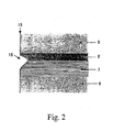
- Fig. 2 shows a diagrammatic view of a section parallel to stripes of a front end face.
- An end face breakdown 16 was induced on a front end face 15 so that a crystal was scooped away in the vicinity of an active layer 7. This scooping of the crystal was the largest in the boundary between the active layer 7 and a cap layer 8.
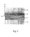
- Fig. 3 shows a diagrammatic view of the section parallel to the stripes of the front end face.
- stage difference 17 is induced so that the stress concentration caused by the lattice mismatching between the crystals of the active layer 7 and the cap layer 8 is relaxed. Then, the possibility that the step 17 and the excessive stress concentration in the boundary between the active layer 7 and the cap layer 8 cause the end face breakdown 16 to be especially centrally induced in the boundary between the active layer 7 and the cap layer 8.
- the active layer 7 is constituted by a multiple quantum well (MQW) structure in which a composition of a well layer is Ga 0.92 In 0.08 N and a composition of a barrier layer is Ga 0.98 In 0.02 N, and the cap layer comprises a mixed crystal of Al 0.15 Ga 0.85 N.
- MQW multiple quantum well
- the lattice mismatchings between the a-axis of the GaN and the free standing mixed crystals of the Ga 0.92 In 0.08 N, the Ga 0.98 In 0.02 N and the Al 0.15 Ga 0.85 N are +0.889 %, +0.222 % and - 0.358 %, respectively. That is, in the boundary from the active layer 7 to the cap layer 8, the lattice mismatching with the GaN is sharply changed from a plus to a minus, which results in the densest concentration of the stress.
- the present inventors obtained the following knowledge. That is, by suppressing the excessive stress concentration caused by the lattice mismatching between the cap layer and the active layer in the vicinity of the active layer 7, it is possible to manufacture the semiconductor laser in which the step 17 does not substantially exist in the boundary between the active layer 7 and the cap layer 8, namely, the semiconductor laser in which the cleaved end face is flat. Also, the end face degradation breakdown induced during the operation can be avoided by suppressing the excessive stress concentration in the vicinity of the active layer on the above-mentioned laser end face and by making the cleaved end face flat.
- the present inventors eagerly discussed a specific method to suppress the excessive stress concentration in the vicinity of the active layer. Then, there was obtained an idea that the excessive stress concentration in the vicinity of the active layer can be suppressed by inserting a stress concentration suppression layer constituted by an Al x Ga 1-x-y In y N (1 > x > 0, 1 > y > 0 and 1 > x+y > 0) mixed crystal layer between the active layer and the cap layer, and by making its composition on the active layer side equal to the composition of the barrier layer of the active layer, namely, the Ga 0.98 In 0.02 N, and on the other hand, by making its composition on the cap layer side equal to the composition of the cap layer, namely, the Al 0.15 Ga 0.85 N, and then by having the composition of the stress concentration suppression layer graded so as to be smoothly changed from the active layer side to the cap layer side.
- a stress concentration suppression layer constituted by an Al x Ga 1-x-y In y N (1 > x > 0, 1 > y > 0 and 1 >
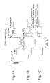
- Fig. 4A shows the diagrammatic view of the band structure in the vicinity of the active layer of the conventional nitride semiconductor laser.
- the band gap between the active layer 7 and the cap layer 8 is large as mentioned above, and the stress concentration is induced in the boundary between the active layer 7 and the cap layer 8.
- Figs. 4B and 4C show the diagrammatic views of the band structure in the vicinity of the active layer of the nitride semiconductor laser according to the present invention.
- a stress concentration suppression layer 47 formed as mentioned above enables the smooth connection from the active layer 7 to the cap layer 8, which is evident from Figs. 4B and 4C, and thereby enables the suppression of the excessive stress concentration in the vicinity of the active layer.
- the present invention relates to:
- the present invention relates to:
- the present invention relates to:
- the present invention relates to:
- the present invention relates to:
- the present invention relates to:
- the present invention relates to:
- the present invention relates to:
- the nitride semiconductor laser implies the semiconductor laser provided with nitride semiconductors.
- the group III element includes any one of the above-mentioned three elements (In, Al and Ga), and the group V element always includes N (nitrogen).
- the above-mentioned GaN-based semiconductor is a concept included in the nitride semiconductor.
- the nitride semiconductor laser in the present invention is characterized by having a stress concentration suppressing layer between an active layer and a cap layer.
- the inclusion of the stress concentration suppressing layer enables the suppression of the stress concentration caused by the lattice mismatching between the active layer and the cap layer.
- the relaxation of the change in the band gap between the active layer and the cap layer enables the suppression of the stress concentration caused by the lattice mismatching between the active layer and the cap layer.
- a nitride semiconductor laser is listed in which it has a stress concentration suppression layer between an active layer and a cap layer, and the stress concentration suppressing layer has, on the active layer, a composition equal to the composition of the active layer, and it has, on the cap layer side, a composition equal to the composition of the cap layer, and the composition of the stress concentration suppressing layer is made graded from the active layer side to the cap layer side, namely, smoothly changed.
- the change of the band gap to the cap layer from the active layer can be relaxed to thereby suppress the stress concentration caused by the lattice mismatching between the active layer and the cap layer.
- the active layer may have any of the known structures. However, if the active layer has the multiple quantum well structure, in the above-mentioned embodiment, a composition of the active layer side of the stress concentration suppressing layer is desired to be equal to a composition of a barrier layer of the active layer.
- the nitride semiconductor laser according to the present invention may have a known structure used in that technical field.
- one embodiment of the nitride semiconductor laser in the present invention includes a semiconductor laser provided with a p-type cladding layer and an n-type cladding, having an active layer of a band gap smaller than those cladding layers between the n-type and p-type cladding layers, a cap layer of a band gap larger than the p-type clad layer between the p-type clad layer and the active layer, and a stress concentration suppressing layer having a function of relaxing the change of the band gap between the active layer and the cap layer between the active layer and the cap layer.
- the p-type cladding layer is desired to be composed of nitride semiconductors containing p-type impurities, for example, Mg and the like.
- the n-type cladding layer is desired to be composed of nitride semiconductors containing n-type impurities, for example, Si and the like.
- nitride semiconductor laser in the present invention includes, for example, a nitride semiconductor laser in which a p-type optical guiding layer is further formed between the p-type cladding layer and the cap layer, and an n-type optical guiding layer is further formed between the active layer and the n-type cladding layer, in the above-mentioned embodiment.
- a band gap of the p-type optical guiding layer is smaller than a band gap of the p-type cladding layer, and a band gap of the n-type optical guiding layer is smaller than a band gap of the n-type cladding layer, and the above-mentioned band gaps of the n-type and p-type optical guiding layers are larger than a band gap of the active layer.
- the p-type optical guiding layer is desired to be composed of the nitride semiconductors containing the p-type impurities, for example, Mg and the like
- the n-type optical guiding layer is desired to be composed of the nitride semiconductors containing the n-type impurities, for example, Si and the like.
- a p-type contact layer may be further formed on a side opposite to the p-type optical guiding layer of the p-type cladding layer, and an n-type contact layer may be further formed on a side opposite to the n-type optical guiding layer of the n-type cladding layer.
- the p-type contact layer is desired to be composed of the nitride semiconductors containing the p-type impurities, for example, Mg and the like.
- the n-type contact layer is desired to be composed of the nitride semiconductors containing the n-type impurities, for example, Si and the like.
- a preferable embodiment of the nitride semiconductor laser according to the present invention includes a nitride semiconductor laser in which it has: an active layer of a multiple quantum well structure having a barrier layer constituted by Ga 1-y1 In y1 N (1 > y1 > 0); a cap layer constituted by Al x1 Ga 1-x1 N (1 > x1 > 0); and a stress concentration suppressing layer constituted by Al x Ga 1-x-y In y N (1 > x > 0, 1 > y > 0, 1 > x+y > 0) between the active layer and the cap layer.
- an atom composition ratio (x, y) between Al and In of the Al x Ga 1-x-y In y N constituting the stress concentration suppressing layer is desired to be graded from (0, y1) to (x1, 0), from the active layer side to the cap layer side, namely, smoothly changed.
- the y1 implies the atom composition ratio of In in the Ga 1-y1 In y1 N constituting the barrier layer
- the x1 implies the atom composition ratio of Al in the Al x1 Ga 1-x1 N constituting the cap layer.
- (x, y) is (0, y1) on a boundary between the stress concentration suppressing layer and the active layer, and it is (x1, 0) on a boundary between the stress concentration suppressing layer and the cap layer, and it further leads to the (x1, 0) from the (0, y1) via a blackly painted region of Fig. 6 within the stress concentration suppressing layer.
- the composition of the stress concentration suppression layer is desired to be smoothly changed within the layer.
- a preferable example includes a case where the inclination of the locus of the (x, y) to the (x1, 0) from the (0, y1) is desired to be always minus, and a more preferable example includes a case where the (x, y) draws in accordance with the locus from (1) to (3) of Fig. 6.
- nitride semiconductor laser of the preferable embodiment according to the present invention if it has the above-mentioned characteristic features, it may have a known structure used in the technical field.
- a more specific embodiment of the nitride semiconductor laser of the above-mentioned preferable embodiment includes, for example, a semiconductor laser in which a lamination structure composed of the active layer, the stress concentration suppressing layer and the cap layer as mentioned above is sandwiched between the n-type cladding layer and the p-type cladding layer. That is, there may be included a semiconductor laser in which the active layer is formed on the n-type cladding layer, the stress concentration suppressing layer is formed on the active layer, the cap layer is formed on the stress concentration suppressing layer, and the p-type cladding layer is formed on the cap layer.
- the compositions of the p-type cladding layer and the n-type cladding layer are not especially limited.
- the n-type cladding layer is desired to be constituted by n-type AlGaN mixed crystals to which Si as the n-type impurity is added, and the p-type cladding layer is desired to comprise p-type AlGaN compound crystals to which Mg as the p-type impurity is added.
- a p-type optical guiding layer may be further formed between the p-type cladding layer and the cap layer, and an n-type optical guiding layer may be further formed between the active layer and the n-type cladding layer.
- a p-type contact layer may be further formed on a side opposite to the p-type optical guiding layer of the p-type cladding layer, and an n-type contact layer may be further formed on a side opposite to the n-type optical guiding layer of the n-type cladding layer.
- the compositions of the above-mentioned respective layers are not especially limited.
- the n-type optical guiding layer is desired to be composed of the n-type GaN to which Si as the n-type impurity is added
- the p-type optical guiding layer is desired to be composed of the p-type GaN to which Mg as the p-type impurity is added.
- the n-type contact layer is desired to be composed of the n-type GaN to which Si as the n-type impurity is added
- the p-type contact layer is desired to be composed of the p-type GaN to which Mg as the p-type impurity is added.
- a manufacturing method of a nitride semiconductor laser according to the present invention may be based on a known method.
- the nitride semiconductor laser according to the present invention can be manufactured by sequentially combining the processes for growing the nitride semiconductor layers constituting the nitride semiconductor laser, under a condition that a lateral direction growth is generated.
- the method of growing the nitride semiconductor layers constituting the nitride semiconductor laser according to the present invention is not especially limited.
- it may use a known method, such as a metal organic chemical vapor deposition (MOCVD) method, a halide vapor phase epitaxy or a molecular beam epitaxy (MBE) method or the like.
- MOCVD metal organic chemical vapor deposition
- MBE molecular beam epitaxy
- Fig. 5 is a cross-sectional view showing the configuration of the nitride semiconductor laser according to the actual embodiment of the present invention.
- a substrate 1 includes a sappier substrate, SiC, Si, GaAs, spinel or ZnO or the like, it is desirable to use the sappier substrate in which a c plane is centrally used.
- a first GaN layer 3 having a thickness of about 1 to 5 ⁇ m, preferably, about 1 to 3 ⁇ m is laminated on the substrate 1 through a buffer layer 2 composed of a nitride semiconductor (for example, GaN, AlN or InGaN or the like) having a lamination direction thickness (hereafter, merely referred to as a thickness) of about 30 nm.
- a nitride semiconductor for example, GaN, AlN or InGaN or the like
- the buffer layer 2 an undoped GaN layer is especially desired.
- the first GaN layer 3 may be an undoped GaN layer or a GaN layer on which impurities are doped, for example, an n-type GaN layer on which n-type impurities such as Si and the like are doped.
- the undoped GaN layer is especially desired.
- the substrate 1, the buffer layer 2 and a part of the first GaN layer are removed, for example, in a shape of stripes, and a second GaN layer 4 is laminated thereon by the ELO method, as shown in Fig. 5.
- the second GaN layer 4 is composed of n-type GaN to which Si as an n-type impurity is added, and it has a role as an n-type cladding layer.
- n-type cladding layer 5 An n-type cladding layer 5, an n-type optical guiding layer 6, an active layer 7, a stress concentration suppressing layer 47, a cap layer 8, a p-type optical guiding layer 9, a p-type cladding layer 10 and a p-type contact layer 11, which act as the nitride semiconductor layers, are sequentially laminated on this second GaN layer 4.
- the n-type cladding layer 5 has a thickness of about 1 ⁇ m, and it comprises an n-type AlGaN mixed crystal to which Si as an n-type impurity is added.
- the n-type optical guiding layer 6 has a thickness of about 0.1 ⁇ m, and it comprises an n-type GaN to which Si as an n-type impurity is added.
- the active layer 7 comprises the GaInN mixed crystal having the multiple quantum well (MQW) structure in which a thickness of a well is about 3 nm and a thickness of a barrier layer is about 4 nm.
- the stress concentration suppressing layer 47 comprises an AlGaInN mixed crystal in which the composition is gradually graded.
- the cap layer 8 is provided in order to protect the active layer 7 from being deteriorated when the upper structure containing the p-type optical guiding layer is formed on the active layer 7. It comprises the AlGaN mixed crystal having a thickness of about 20 nm.
- the p-type optical guiding layer 9 has a thickness of about 0.1 ⁇ m, and it comprises a p-type GaN to which Mg as a p-type impurity is added.
- the p-type cladding layer 10 has a thickness of about 0.5 ⁇ m, and it comprises a p-type AlGaN mixed crystal to which Mg as a p-type impurity is added.
- the p-type cladding layer 10 may comprise a super lattice structure composed of an AlGaN layer and a GaN layer.
- the p-type contact layer 11 has a thickness of about 0.1 ⁇ m, and it comprises a p-type GaN to which Mg as a p-type impurity is added.
- the upper portion of the p-type cladding layer 10 and the p-type contact layer 11 may be processed as the upper mesa structure whose cross-sectional shape is tapered and striped in order to attain a current confinement.
- a p-side electrode 13 is formed on the p-type contact layer 11 through an opening formed on the insulating layer 12.
- the p-side electrode 13 is configured such that palladium (Pd), platinum (Pt) and gold (Au) are sequentially laminated from the side of the p-type contact layer 11.
- this p-side electrode 13 is formed in a shape of a slender band (a shape of a band extended in a direction vertical to the drawing in Fig. 5) in order to attain the current confinement.
- an n-side electrode 14 in which titanium (Ti), aluminum (Al) and gold (Au) are sequentially laminated is formed on the second GaN layer 4.
- reflection mirror layers are formed on a pair of sides vertical to a length direction (namely, a resonator length direction) of the p-side electrode 13, respectively.
- the manufacturing method of the above-mentioned nitride semiconductor laser will be described below.
- the above-mentioned manufacturing method is one of the specific embodiments of the manufacturing method of the nitride semiconductor laser according to the present invention.
- This manufacturing method carries out a known pretreatment, such as an operation for washing a surface of the substrate 1 through a thermal cleaning and the like, depending on a desire.
- the buffer layer 2 is grown on the substrate 1 by the MOCVD method.
- a growth temperature of the buffer layer 2 is desired to be a temperature lower than a growth temperature of the first GaN layer 3 as described later, specifically, a temperature of about 520°C.
- the first GaN layer 3 is grown on the buffer layer 2 by the MOCVD method.
- the growth temperature of the first GaN layer 3 is, for example, about 900° C to 1100° C, preferably, about 1000° C.
- a film thickness of the first GaN layer 3 is not especially limited. However, it is properly set such that a concave convex structure shown in Fig. 5 can be formed. Since a cycle of the concave convex structure is desired to be about 3 to 25 ⁇ m, it is desirable to form the first GaN layer 3 at a film thickness of about 1 to 5 ⁇ m.
- a mask formation film for a protective film mask formation is formed on the first GaN layer 3, and it is patterned to thereby form a protective film mask (not shown) of a predetermined pattern.
- the technique such as a CVD method, a deposition method, a sputtering method or the like is used to form the mask formation film on the first GaN layer 3 and then form a resist film on the mask formation film.
- the predetermined pattern is exposed and developed to thereby form a resist pattern to which the pattern is transferred.
- the pattern is not especially limited if it is shaped such that a part of the first GaN layer corresponding to the concave portion of the formed concave convex structure is exposed.
- the shapes of stripes, zigzags, dots, grids and the like are included.
- a stripe width is desired to be about 0.5 to 20 ⁇ m
- a stripe interval is desired to be about 1 to 25 ⁇ m.
- a thickness of the protective film is not especially limited. However, it is desirable to be about 1 ⁇ m or less in view of the easiness of the process.
- the material of the mask formation film is not especially limited if it is the material having the property that disables the nitride semiconductor layer to be grown on the protective film or causes the growth to be difficult.
- SiO x , SiN x , TiN, TiO, W and the like may be used.
- the upper layer portion of the substrate and the first GaN layer exposed from the protective film mask are selectively etched and removed. After that, the protective film mask is removed. Then, the concave convex structure having the concave portion in which the substrate is exposed and the convex portion composed of the first GaN layer 3 and the upper portion of the substrate 1 is formed on the substrate surface.
- the etched amount of the substrate is desired to be about 2 ⁇ m or less, preferably, about 0.2 ⁇ m.
- the cross-sectional shape of the convex portion formed by the etching may be tapered. However, it is desirable to be a vertical plane.
- the etching method includes the methods such as a wet etching method, a dry etching method and the like. However, the dry etching method is desired.
- the dry etching method includes, in specific, a reactive ion dry etching (RIE) method, a reactive ion beam dry etching (RIBE) method, for example.
- RIE reactive ion dry etching
- RIBE reactive ion beam dry etching
- the substrate is fed into the MOCVD apparatus and, under a condition that the lateral direction growth is generated, the n-type second GaN layer 4, the n-type cladding layer 5 composed of the n-type AlGaN, the n-type optical guiding layer 6 composed of the n-type GaN, the active layer 7, the stress concentration suppressing layer 47, the cap layer 8, the p-type optical guiding layer 9 composed of the p-type GaN, the p-type cladding layer 10 composed of the p-type AlGaN and the p-type contact layer 11 composed of the p-type GaN are sequentially laminated.
- the active layer 7 having the multiple quantum well structure in which a GaInN layer acts as a light emission layer is formed.
- the stress concentration suppression layer 47 in which it is composed of an AlGaIn layer and its composition is graded, is formed.
- the p-type AlGaN cap layer 8 is formed thereon at a relatively low temperature.
- the In composition in the active layer constituted by the GaInN multiple quantum well structure is desired to be adjusted to, for example, about 0.08 in the well layer, and for example, about 0.02 in the barrier layer. Also, it is desirable to adjust the Al composition ratio in the cap layer composed of AlGaN to, for example, about 0.15.
- the stress concentration suppressing layer 47 When the active layer and the cap layer are set in this way, in such a way that the atomic composition ratio (x, y) of Al and In in Al x Ga 1-x-y In y N of the stress concentration suppressing layer 47 has the value of (0, 0.02) equal to the composition of the barrier layer of the active layer, on the active layer side, and it has the value of (0.15, 0) equal to the composition of the cap layer, on the cap layer side, the stress concentration suppression layer 47 is grown.
- tri-methyl gallium ((CH 3 ) 3 Ga : TMG) as a raw material of Ga of the group III element
- tri-methyl aluminum ((CH 3 ) 3 Al : TMAl) as a raw material of Al of the group III element
- tri-methyl indium ((CH 3 ) 3 In : TMIn) as a raw material of In of the group III element
- ammonium (NH 3 ) as a raw material of N of the group V element.
- a carrier gas it is desirable to use, for example, a mixture gas of hydrogen (H 2 ) and nitrogen (N 2 ).
- n-type dopant for example, mono-silane
- the substrate on which the nitride semiconductor layer is grown is again taken away from the MOCVD apparatus.
- the insulating layer 12 made of SiO 2 is formed on the p-type contact layer 11 composed of the p-type GaN, for example, by the CVD method.
- a resist film (not shown) is coated on the insulating layer 12, and a mask pattern corresponding to a formation position of a p-side electrode 13 is formed by a photo-lithography. After that, this is used to etch, and the insulating layer 12 is selectively removed, and an opening corresponding to the formation position of the p-side electrode 13 is formed.
- palladium (Pd), platinum (Pt) and gold (Au) are sequentially deposited on the entire surface (namely, on the p-type contact layer 11 made of the p-type GaN from which the insulating layer 12 is selectively removed and on the resist film (not shown)). Then, the resist film (not shown) together with the palladium, the platinum and the gold, which are deposited on this resist film, is removed (lifted off) to thereby form the p-side electrode 13.
- the insulating layer 12, the p-type contact layer 11, the p-type cladding layer 10, the p-type optical guiding layer 9, the cap layer 8, the stress concentration suppressing layer 47, the active layer 7, the n-type optical guiding layer 6 and the n-type cladding layer 5 are removed sequentially and selectively.
- titanium, aluminum and gold are selectively deposited on the second GaN layer 4, and the n-side electrode 14 is formed.
- the substrate 1 is cleaved at a predetermined width, vertically to the length direction (the resonator length direction) of the p-side electrode 13, and the reflection mirror layer is formed on the cleaved surface. Consequently, the nitride semiconductor laser according to the present invention is formed as shown in Fig. 5.
- the above-mentioned manufacturing method has been described by limiting the growing method to the MOCVD method. However, it may be grown by using the other vapor phase growing methods, such as the halide vapor phase epitaxy or the molecular beam epitaxy (MBE) method or the like.
- the other vapor phase growing methods such as the halide vapor phase epitaxy or the molecular beam epitaxy (MBE) method or the like.
- the introduction of the stress concentration suppressing layer composed of the graded composition AlGaInN mixed crystal enables the suppression of the concentration of the stress in the boundary between the active layer and the cap layer (hereafter, referred to as the active layer/cap layer boundary).
- the active layer/cap layer boundary the occurrence of the stage difference in the active layer/cap layer boundary can be suppressed on the cleaved end face.
- the stress concentration in the active layer/cap layer boundary is suppressed to thereby enable the suppression of the progress of the end face breakdown. As a result, it is possible to prolong the life of the semiconductor laser.
Landscapes
- Physics & Mathematics (AREA)
- Optics & Photonics (AREA)
- Chemical & Material Sciences (AREA)
- Engineering & Computer Science (AREA)
- Nanotechnology (AREA)
- Condensed Matter Physics & Semiconductors (AREA)
- General Physics & Mathematics (AREA)
- Electromagnetism (AREA)
- Life Sciences & Earth Sciences (AREA)
- Biophysics (AREA)
- Crystallography & Structural Chemistry (AREA)
- Semiconductor Lasers (AREA)
Abstract
Description
Claims (24)
- A nitride semiconductor laser characterized by having a stress concentration suppressing layer between an active layer and a cap layer.
- The nitride semiconductor laser according to claim 1, characterized in that the stress concentration suppressing layer has a function of relaxing a change in a band gap between the active layer and the cap layer.
- The nitride semiconductor laser according to claim 1, characterized in that:the stress concentration suppressing layer has, on an active layer side, a composition identical to the active layer, and on a cap layer side, a composition identical to the cap layer, andthe composition of the stress concentration suppressing layer is graded to the cap layer side from the active layer side.
- The nitride semiconductor laser according to claim 3, characterized in that the composition on the active layer side of the stress concentration suppressing layer has a composition identical to a barrier layer of the active layer having a multiple quantum well structure.
- The nitride semiconductor laser according to claim 1, characterized in that:the active layer has a multiple quantum well structure;a barrier layer thereof comprises Ga1-y1Iny1N (1 > y1 > 0);the cap layer comprises Alx1Ga1-x1N (1 > x1 > 0); andthe stress concentration suppressing layer comprises AlxGa1-x-yInyN (1 > x > 0, 1 > y > 0, 1 > x+y > 0).
- The nitride semiconductor laser according to claim 5, characterized in that an atom composition ratio (x, y) of Al and In in the AlxGa1-x-yInyN (1 > x > 0, 1 > y > 0, 1 > x+y > 0) constituting the stress concentration suppressing layer is graded from (0, y1) (the y1 indicates an atom composition ratio of In in the Ga1- y1Iny1N constituting the barrier layer, and satisfies (1 > y1 > 0)) to (x1, 0) (the x1 indicates an atom composition ratio of Al in the Alx1Ga1-x1N constituting the cap layer, and satisfies (1 > x1 > 0)), from the active layer side to the cap layer side.
- The nitride semiconductor laser according to claim 2, characterized by comprising:an n-type cladding layer on a side opposite to the stress concentration suppressing layer of the active layer; anda p-type cladding layer on a side opposite to the stress concentration suppression layer of the cap layer, and characterized in that:a band gap of the active layer is smaller than band gaps of said n-type and p-type cladding layers; anda band gap of the cap layer is larger than the band gap of the p-type cladding layer.
- The nitride semiconductor laser according to claim 7, characterized in that:the n-type cladding layer comprises an n-type AlGaN mixed crystal containing Si as n-type impurities; andthe p-type cladding layer comprises a p-type AlGaN mixed crystal containing Mg as p-type impurities.
- The nitride semiconductor laser according to claim 7, characterized in that:an n-type optical guiding layer is further formed between the active layer and the n-type cladding layer; anda p-type optical guiding layer is further formed between the p-type cladding layer and the cap layer.
- The nitride semiconductor laser according to claim 9, characterized in that:the n-type optical guiding layer comprises an n-type GaN containing Si as n-type impurities; andthe p-type optical guiding layer comprises a p-type GaN containing Mg as p-type impurities.
- The nitride semiconductor laser according to claim 9, characterized in that:an n-type contact layer is further formed on a side opposite to the n-type optical guiding layer of the n-type cladding layer; anda p-type contact layer is further formed on a side opposite to the p-type optical guiding layer of the p-type cladding layer.
- The nitride semiconductor laser according to claim 11, characterized in that:the n-type contact layer comprises an n-type GaN containing Si as n-type impurities; andthe p-type contact layer comprises a p-type GaN containing Mg as p-type impurities.
- A manufacturing method of a nitride semiconductor laser, characterized by comprising:a step of growing a stress concentration suppressing layer on an active layer; anda step of growing a cap layer on the stress concentration suppressing layer.
- The manufacturing method of a nitride semiconductor laser according to claim 13, characterized in that the stress concentration suppressing layer has a function of relaxing a change in a band gap between the active layer and the cap layer.
- The manufacturing method of a nitride semiconductor laser according to claim 13, characterized in that:the stress concentration suppressing layer has, on an active layer side, a composition identical to the active layer, and on a cap layer side, a composition identical to the cap layer; andthe composition of the stress concentration suppressing layer is graded to the cap layer side from the active layer side.
- The manufacturing method of a nitride semiconductor laser according to claim 15, characterized in that the composition on the active layer side of the stress concentration suppressing layer has a composition identical to a barrier layer of the active layer having a multiple quantum well structure.
- The manufacturing method of a nitride semiconductor laser according to claim 13, characterized in that:the active layer has a multiple quantum well structure;a barrier layer thereof comprises Ga1-y1Iny1N (1 > y1 > 0);the cap layer comprises Alx1Ga1-x1N (1 > x1 > 0); andthe stress concentration suppressing layer comprises AlxGa1-x-yInyN (1 > x > 0, 1 > y > 0, 1 > x+y > 0).
- The manufacturing method of a nitride semiconductor laser according to claim 17, characterized in that an atom composition ratio (x, y) of Al and In in the AlxGa1-x-yInyN (1 > x > 0, 1 > y > 0, 1 > x+y > 0) constituting the stress concentration suppression layer is graded from (0, y1) (the y1 indicates an atom composition ratio of In in the Ga1-y1Iny1N constituting the barrier layer, and satisfies (1 > y1 > 0)) to (x1, 0) (the x1 indicates an atom composition ratio of Al in the Alx1Ga1-x1N constituting the cap layer, and satisfies (1 > x1 > 0)), from the active layer side to the cap layer side.
- The manufacturing method of a nitride semiconductor laser according to claim 13, characterized by further comprising:a step of growing the active layer on an n-type cladding layer; anda step of growing a p-type cladding layer on the cap layer, and characterized in that:a band gap of the active layer is smaller than band gaps of said n-type and p-type cladding layers; anda band gap of the cap layer is larger than the band gap of the p-type cladding layer.
- The manufacturing method of a nitride semiconductor laser according to claim 19, characterized in that:the n-type cladding layer comprises an n-type AlGaN mixed crystal containing Si as n-type impurities; andthe p-type cladding layer comprises a p-type AlGaN mixed crystal containing Mg as p-type impurities.
- The manufacturing method of a nitride semiconductor laser according to claim 13, characterized by comprising:a step of growing an n-type optical guiding layer on an n-type cladding layer;a step of growing the active layer on the n-type optical guiding layer;a step of growing a p-type optical guiding layer on the cap layer; anda step of growing a p-type cladding layer on the p-type optical guiding layer.
- The manufacturing method of a nitride semiconductor laser according to claim 21, characterized in that:the n-type optical guiding layer comprises n-type GaN containing Si as n-type impurities; andthe p-type optical guiding layer comprises p-type GaN containing Mg as p-type impurities.
- The manufacturing method of a nitride semiconductor laser according to claim 21, characterized by further comprising:a step of growing the n-type cladding layer on an n-type contact layer; anda step of growing a p-type contact layer on the p-type cladding layer.
- The manufacturing method of a nitride semiconductor laser according to claim 23, characterized in that:the n-type contact layer comprises an n-type GaN containing Si as n-type impurities; andthe p-type contact layer comprises a p-type GaN containing Mg as p-type impurities.
Applications Claiming Priority (3)
| Application Number | Priority Date | Filing Date | Title |
|---|---|---|---|
| JP2001169440 | 2001-06-05 | ||
| JP2001169440A JP3876649B2 (en) | 2001-06-05 | 2001-06-05 | Nitride semiconductor laser and manufacturing method thereof |
| PCT/JP2002/005509 WO2002099942A1 (en) | 2001-06-05 | 2002-06-04 | Nitride semiconductor laser |
Publications (3)
| Publication Number | Publication Date |
|---|---|
| EP1394912A1 true EP1394912A1 (en) | 2004-03-03 |
| EP1394912A4 EP1394912A4 (en) | 2007-02-21 |
| EP1394912B1 EP1394912B1 (en) | 2009-12-02 |
Family
ID=19011510
Family Applications (1)
| Application Number | Title | Priority Date | Filing Date |
|---|---|---|---|
| EP02730913A Expired - Lifetime EP1394912B1 (en) | 2001-06-05 | 2002-06-04 | Nitride semiconductor laser |
Country Status (6)
| Country | Link |
|---|---|
| US (3) | US6891268B2 (en) |
| EP (1) | EP1394912B1 (en) |
| JP (1) | JP3876649B2 (en) |
| CN (1) | CN1203598C (en) |
| DE (1) | DE60234590D1 (en) |
| WO (1) | WO2002099942A1 (en) |
Families Citing this family (34)
| Publication number | Priority date | Publication date | Assignee | Title |
|---|---|---|---|---|
| US6958497B2 (en) * | 2001-05-30 | 2005-10-25 | Cree, Inc. | Group III nitride based light emitting diode structures with a quantum well and superlattice, group III nitride based quantum well structures and group III nitride based superlattice structures |
| US7692182B2 (en) * | 2001-05-30 | 2010-04-06 | Cree, Inc. | Group III nitride based quantum well light emitting device structures with an indium containing capping structure |
| US8545629B2 (en) | 2001-12-24 | 2013-10-01 | Crystal Is, Inc. | Method and apparatus for producing large, single-crystals of aluminum nitride |
| KR20050054482A (en) * | 2002-06-26 | 2005-06-10 | 암모노 에스피. 제트오. 오. | Nitride semiconductor laser device and a method for improving its performance |
| KR101020387B1 (en) * | 2002-12-20 | 2011-03-08 | 크리 인코포레이티드 | Electronic device including semiconductor mesa structure and conductive junction and method for manufacturing same |
| TW587346B (en) * | 2003-03-28 | 2004-05-11 | United Epitaxy Co Ltd | Optoelectronic device made by semiconductor compound |
| KR101034055B1 (en) | 2003-07-18 | 2011-05-12 | 엘지이노텍 주식회사 | Light emitting diodes and manufacturing method |
| GB2407700A (en) * | 2003-10-28 | 2005-05-04 | Sharp Kk | MBE growth of nitride semiconductor lasers |
| EP1821378A4 (en) * | 2004-12-08 | 2009-12-09 | Sumitomo Electric Industries | SEMICONDUCTOR LASER DEVICE AND METHOD OF MANUFACTURING THE SAME |
| US20070025106A1 (en) * | 2005-07-29 | 2007-02-01 | Korry Electronics Co. | Night vision compatible area light fixture |
| WO2007040295A1 (en) * | 2005-10-04 | 2007-04-12 | Seoul Opto Device Co., Ltd. | (al, ga, in)n-based compound semiconductor and method of fabricating the same |
| KR101111720B1 (en) * | 2005-10-12 | 2012-02-15 | 삼성엘이디 주식회사 | Side-emitting semiconductor laser diode with a dielectric layer formed on the active layer |
| TW200735418A (en) * | 2005-11-22 | 2007-09-16 | Rohm Co Ltd | Nitride semiconductor device |
| US7641735B2 (en) | 2005-12-02 | 2010-01-05 | Crystal Is, Inc. | Doped aluminum nitride crystals and methods of making them |
| US9034103B2 (en) | 2006-03-30 | 2015-05-19 | Crystal Is, Inc. | Aluminum nitride bulk crystals having high transparency to ultraviolet light and methods of forming them |
| US7804869B2 (en) * | 2006-05-22 | 2010-09-28 | Agere Systems Inc. | Gallium nitride based semiconductor device with electron blocking layer |
| US20080137701A1 (en) * | 2006-12-12 | 2008-06-12 | Joseph Michael Freund | Gallium Nitride Based Semiconductor Device with Reduced Stress Electron Blocking Layer |
| TW200828624A (en) * | 2006-12-27 | 2008-07-01 | Epistar Corp | Light-emitting diode and method for manufacturing the same |
| US9771666B2 (en) | 2007-01-17 | 2017-09-26 | Crystal Is, Inc. | Defect reduction in seeded aluminum nitride crystal growth |
| WO2008088838A1 (en) | 2007-01-17 | 2008-07-24 | Crystal Is, Inc. | Defect reduction in seeded aluminum nitride crystal growth |
| US8080833B2 (en) * | 2007-01-26 | 2011-12-20 | Crystal Is, Inc. | Thick pseudomorphic nitride epitaxial layers |
| JP4927606B2 (en) * | 2007-03-08 | 2012-05-09 | 古河電気工業株式会社 | Semiconductor light emitting device |
| KR101265641B1 (en) * | 2007-05-15 | 2013-05-22 | 엘지전자 주식회사 | Semiconductor light emiting device and method for making the same |
| JP5083817B2 (en) * | 2007-11-22 | 2012-11-28 | シャープ株式会社 | Group III nitride semiconductor light-emitting device and method for manufacturing the same |
| DE102009015569B9 (en) | 2009-03-30 | 2023-06-29 | OSRAM Opto Semiconductors Gesellschaft mit beschränkter Haftung | Optoelectronic semiconductor chip |
| US8536615B1 (en) | 2009-12-16 | 2013-09-17 | Cree, Inc. | Semiconductor device structures with modulated and delta doping and related methods |
| US8604461B2 (en) * | 2009-12-16 | 2013-12-10 | Cree, Inc. | Semiconductor device structures with modulated doping and related methods |
| US8575592B2 (en) * | 2010-02-03 | 2013-11-05 | Cree, Inc. | Group III nitride based light emitting diode structures with multiple quantum well structures having varying well thicknesses |
| JP5806734B2 (en) | 2010-06-30 | 2015-11-10 | クリスタル アイエス, インコーポレーテッドCrystal Is, Inc. | Large single crystal growth of aluminum nitride by thermal gradient control |
| CN103180973A (en) * | 2010-11-02 | 2013-06-26 | 皇家飞利浦电子股份有限公司 | Iii-nitride light emitting device |
| JP4971508B1 (en) * | 2011-01-21 | 2012-07-11 | 住友電気工業株式会社 | Group III nitride semiconductor laser device and method of manufacturing group III nitride semiconductor laser device |
| US8962359B2 (en) | 2011-07-19 | 2015-02-24 | Crystal Is, Inc. | Photon extraction from nitride ultraviolet light-emitting devices |
| JP2012156518A (en) * | 2012-03-08 | 2012-08-16 | Sumitomo Electric Ind Ltd | Group iii nitride semiconductor laser element and method of manufacturing group iii nitride semiconductor laser element |
| EP2973664B1 (en) | 2013-03-15 | 2020-10-14 | Crystal Is, Inc. | Ultraviolet light-emitting device and method of forming a contact to an ultraviolet light-emitting device |
Family Cites Families (23)
| Publication number | Priority date | Publication date | Assignee | Title |
|---|---|---|---|---|
| JP2900946B2 (en) | 1990-03-15 | 1999-06-02 | 富士通株式会社 | Semiconductor device |
| US5670798A (en) | 1995-03-29 | 1997-09-23 | North Carolina State University | Integrated heterostructures of Group III-V nitride semiconductor materials including epitaxial ohmic contact non-nitride buffer layer and methods of fabricating same |
| US5625202A (en) * | 1995-06-08 | 1997-04-29 | University Of Central Florida | Modified wurtzite structure oxide compounds as substrates for III-V nitride compound semiconductor epitaxial thin film growth |
| JP3635757B2 (en) * | 1995-12-28 | 2005-04-06 | 昭和電工株式会社 | AlGaInP light emitting diode |
| JP3304782B2 (en) * | 1996-09-08 | 2002-07-22 | 豊田合成株式会社 | Semiconductor light emitting device |
| US5834331A (en) | 1996-10-17 | 1998-11-10 | Northwestern University | Method for making III-Nitride laser and detection device |
| US6258619B1 (en) * | 1996-12-06 | 2001-07-10 | Rohm Ltd | Fabrication of semiconductor light emitting device |
| CN100485984C (en) * | 1997-01-09 | 2009-05-06 | 日亚化学工业株式会社 | Nitride semiconductor device |
| JP3679914B2 (en) * | 1997-02-12 | 2005-08-03 | 株式会社東芝 | Semiconductor light emitting device and manufacturing method thereof |
| JP3433038B2 (en) | 1997-02-24 | 2003-08-04 | 株式会社東芝 | Semiconductor light emitting device |
| JPH10242579A (en) * | 1997-02-27 | 1998-09-11 | Sharp Corp | Nitride III-V compound semiconductor device |
| GB2327145A (en) | 1997-07-10 | 1999-01-13 | Sharp Kk | Graded layers in an optoelectronic semiconductor device |
| JPH1168158A (en) * | 1997-08-20 | 1999-03-09 | Sanyo Electric Co Ltd | Gallium nitride based compound semiconductor device |
| US6160833A (en) * | 1998-05-06 | 2000-12-12 | Xerox Corporation | Blue vertical cavity surface emitting laser |
| US6218280B1 (en) * | 1998-06-18 | 2001-04-17 | University Of Florida | Method and apparatus for producing group-III nitrides |
| US6233265B1 (en) * | 1998-07-31 | 2001-05-15 | Xerox Corporation | AlGaInN LED and laser diode structures for pure blue or green emission |
| JP2000077783A (en) | 1998-08-27 | 2000-03-14 | Nec Corp | Growth method of indium-containing nitride semiconductor crystal |
| JP4530234B2 (en) * | 1998-10-09 | 2010-08-25 | シャープ株式会社 | Semiconductor light emitting device |
| JP3796065B2 (en) | 1999-05-24 | 2006-07-12 | 三洋電機株式会社 | Light emitting device and manufacturing method thereof |
| JP2001007379A (en) * | 1999-06-24 | 2001-01-12 | Sharp Corp | Gallium nitride based compound semiconductor photo detector |
| JP3778765B2 (en) * | 2000-03-24 | 2006-05-24 | 三洋電機株式会社 | Nitride-based semiconductor device and manufacturing method thereof |
| EP1364537A4 (en) * | 2000-12-28 | 2005-12-14 | Thomson Licensing | On screen display as diagnostic aid |
| JP2003063897A (en) * | 2001-08-28 | 2003-03-05 | Sony Corp | Nitride III-V compound semiconductor substrate, method of manufacturing the same, method of manufacturing semiconductor light emitting element, and method of manufacturing semiconductor device |
-
2001
- 2001-06-05 JP JP2001169440A patent/JP3876649B2/en not_active Expired - Lifetime
-
2002
- 2002-06-04 US US10/343,878 patent/US6891268B2/en not_active Expired - Lifetime
- 2002-06-04 EP EP02730913A patent/EP1394912B1/en not_active Expired - Lifetime
- 2002-06-04 DE DE60234590T patent/DE60234590D1/en not_active Expired - Lifetime
- 2002-06-04 CN CNB028024494A patent/CN1203598C/en not_active Expired - Fee Related
- 2002-06-04 WO PCT/JP2002/005509 patent/WO2002099942A1/en not_active Ceased
-
2005
- 2005-03-24 US US11/090,749 patent/US20050167836A1/en not_active Abandoned
- 2005-03-25 US US11/090,340 patent/US7135772B2/en not_active Expired - Fee Related
Also Published As
| Publication number | Publication date |
|---|---|
| JP3876649B2 (en) | 2007-02-07 |
| US20050167836A1 (en) | 2005-08-04 |
| US7135772B2 (en) | 2006-11-14 |
| CN1203598C (en) | 2005-05-25 |
| US20050167835A1 (en) | 2005-08-04 |
| CN1465123A (en) | 2003-12-31 |
| EP1394912B1 (en) | 2009-12-02 |
| DE60234590D1 (en) | 2010-01-14 |
| US20040012011A1 (en) | 2004-01-22 |
| EP1394912A4 (en) | 2007-02-21 |
| US6891268B2 (en) | 2005-05-10 |
| JP2002368343A (en) | 2002-12-20 |
| WO2002099942A1 (en) | 2002-12-12 |
Similar Documents
| Publication | Publication Date | Title |
|---|---|---|
| US6891268B2 (en) | Nitride semiconductor laser | |
| KR101083872B1 (en) | Baan-based III-VIII compound semiconductor light emitting device and method of manufacturing the same | |
| EP1184913B1 (en) | Nitride semiconductor laser diode | |
| US6920166B2 (en) | Thin film deposition method of nitride semiconductor and nitride semiconductor light emitting device | |
| JP4288743B2 (en) | Nitride semiconductor growth method | |
| US6455877B1 (en) | III-N compound semiconductor device | |
| JP5743424B2 (en) | Nitride semiconductor structure, manufacturing method thereof, and light emitting device | |
| US20020110945A1 (en) | Optical semiconductor device having an epitaxial layer of iii-v compound semiconductor material containing n as a group v element | |
| JP2001267242A (en) | Group III nitride compound semiconductor and method of manufacturing the same | |
| JP2001196699A (en) | Semiconductor element | |
| JP2001267691A (en) | Semiconductor device and method of manufacturing the same | |
| JPH1174621A (en) | Nitride based semiconductor light emitting device | |
| EP2728684A1 (en) | Gallium nitride semiconductor laser element and method for manufacturing gallium nitride semiconductor laser element | |
| JP2002270971A (en) | Nitride semiconductor device | |
| JP4631214B2 (en) | Manufacturing method of nitride semiconductor film | |
| JP2001044570A (en) | Nitride semiconductor laser device | |
| JP4016062B2 (en) | Nitride semiconductor structure, manufacturing method thereof, and light emitting device | |
| JP4712241B2 (en) | Semiconductor laser device and manufacturing method thereof | |
| JP3717255B2 (en) | Group 3 nitride semiconductor laser device | |
| JP5449819B2 (en) | Nitride semiconductor thick film substrate | |
| JP3438675B2 (en) | Method for growing nitride semiconductor | |
| JP4394800B2 (en) | Nitride III-V compound semiconductor device and manufacturing method thereof | |
| JP5080820B2 (en) | Nitride semiconductor structure, manufacturing method thereof, and light emitting device | |
| JP3987879B2 (en) | Nitride semiconductor light emitting device and manufacturing method thereof | |
| JP3950471B2 (en) | Nitride semiconductor structure, manufacturing method thereof, and light emitting device |
Legal Events
| Date | Code | Title | Description |
|---|---|---|---|
| PUAI | Public reference made under article 153(3) epc to a published international application that has entered the european phase |
Free format text: ORIGINAL CODE: 0009012 |
|
| 17P | Request for examination filed |
Effective date: 20030121 |
|
| AK | Designated contracting states |
Kind code of ref document: A1 Designated state(s): AT BE CH CY DE DK ES FI FR GB GR IE IT LI LU MC NL PT SE TR |
|
| A4 | Supplementary search report drawn up and despatched |
Effective date: 20070122 |
|
| 17Q | First examination report despatched |
Effective date: 20070705 |
|
| GRAP | Despatch of communication of intention to grant a patent |
Free format text: ORIGINAL CODE: EPIDOSNIGR1 |
|
| GRAS | Grant fee paid |
Free format text: ORIGINAL CODE: EPIDOSNIGR3 |
|
| GRAA | (expected) grant |
Free format text: ORIGINAL CODE: 0009210 |
|
| AK | Designated contracting states |
Kind code of ref document: B1 Designated state(s): DE FR GB |
|
| REG | Reference to a national code |
Ref country code: GB Ref legal event code: FG4D |
|
| REF | Corresponds to: |
Ref document number: 60234590 Country of ref document: DE Date of ref document: 20100114 Kind code of ref document: P |
|
| PLBE | No opposition filed within time limit |
Free format text: ORIGINAL CODE: 0009261 |
|
| STAA | Information on the status of an ep patent application or granted ep patent |
Free format text: STATUS: NO OPPOSITION FILED WITHIN TIME LIMIT |
|
| 26N | No opposition filed |
Effective date: 20100903 |
|
| REG | Reference to a national code |
Ref country code: GB Ref legal event code: 746 Effective date: 20120702 |
|
| REG | Reference to a national code |
Ref country code: DE Ref legal event code: R084 Ref document number: 60234590 Country of ref document: DE Effective date: 20120614 |
|
| PGFP | Annual fee paid to national office [announced via postgrant information from national office to epo] |
Ref country code: GB Payment date: 20140618 Year of fee payment: 13 |
|
| PGFP | Annual fee paid to national office [announced via postgrant information from national office to epo] |
Ref country code: DE Payment date: 20140619 Year of fee payment: 13 |
|
| PGFP | Annual fee paid to national office [announced via postgrant information from national office to epo] |
Ref country code: FR Payment date: 20140619 Year of fee payment: 13 |
|
| REG | Reference to a national code |
Ref country code: DE Ref legal event code: R119 Ref document number: 60234590 Country of ref document: DE |
|
| GBPC | Gb: european patent ceased through non-payment of renewal fee |
Effective date: 20150604 |
|
| REG | Reference to a national code |
Ref country code: FR Ref legal event code: ST Effective date: 20160229 |
|
| PG25 | Lapsed in a contracting state [announced via postgrant information from national office to epo] |
Ref country code: DE Free format text: LAPSE BECAUSE OF NON-PAYMENT OF DUE FEES Effective date: 20160101 Ref country code: GB Free format text: LAPSE BECAUSE OF NON-PAYMENT OF DUE FEES Effective date: 20150604 |
|
| PG25 | Lapsed in a contracting state [announced via postgrant information from national office to epo] |
Ref country code: FR Free format text: LAPSE BECAUSE OF NON-PAYMENT OF DUE FEES Effective date: 20150630 |